


 |
市場調查報告書
商品編碼
2099753
HBM 8層堆疊與12層堆疊:市場佔有率分析、產業趨勢與統計、成長預測(2026-2031年)HBM 8-Hi Vs 12-Hi Stack - Market Share Analysis, Industry Trends & Statistics, Growth Forecasts (2026 - 2031) |
||||||

※ 本網頁內容可能與最新版本有所差異。詳細情況請與我們聯繫。
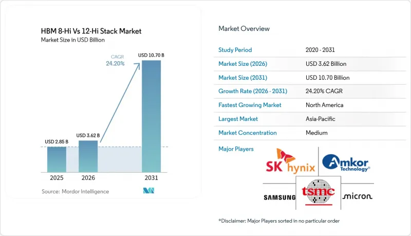
根據 Mordor Intelligence 預測,HBM 8-Hi 和 12-Hi 堆疊市場預計將從 2025 年的 28.5 億美元成長到 2026 年的 36.2 億美元,到 2031 年達到 107 億美元,預計 2026 年至 2031 年的複合年成長率為 2031%。
本報告按應用領域(伺服器、網路、高效能運算等)、技術(HBM2、HBM2E、HBM3等)、單棧記憶體容量(最高可達8GB、16GB、24GB、36GB等)、處理器介面(GPU、CPU、AI加速器和ASIC、FPGA等)以及地區(北美、亞太等)進行細分。市場預測以美元(USD)計價。
全球 HBM 8 層與 12 層堆疊市場趨勢及洞察
人工智慧加速器頻寬的快速擴展
隨著每一代主流加速器的推出,用於人工智慧訓練和推理的最低記憶體頻寬要求不斷提高,這項變化正推動HBM 8-Hi與12-Hi堆疊市場加速升級。 NVIDIA的Rubin平台已將HBM4的總頻寬提升至遠超過以往系統的水平。這加大了記憶體供應商的壓力,要求他們在不延長認證週期的情況下提供更高效能的堆疊。美光宣布,到2025年底,其HBM4產品的運行速度將超過11 Gbps,量產速度遠超HBM3E。這表明,更高的引腳速度不再是實驗室的里程碑,而已成為商業性需求。這項轉變意義重大,因為HBM 8-Hi與12-Hi堆疊市場現在首先響應加速器藍圖,供應藍圖的計畫也隨之調整。此外,高速堆疊需要更嚴格的製程控制、更快的認證以及與GPU和ASIC開發週期更緊密的協調,從而提高了新進入者的進入門檻。因此,隨著平台供應商針對各種系統需求進行最佳化,對高速8層堆疊和高容量12層堆疊的需求都在迅速成長。
主要GPU平台對HBM4認證的需求
旗艦GPU認證專案是HBM 8層與12層堆疊市場競爭中最明確的商業性促進因素之一。 JEDEC於2025年4月正式發布了HBM4標準,為供應商和晶片設計人員提供了一個通用的2048位元介面和32個獨立通道框架。 2025年3月,SK海力士採用其先進的MR-MUF製程向客戶交付了首批12層HBM4樣品,在下一個平台週期中搶佔了先機。隨後,三星於2026年2月開始基於4nm邏輯晶片量產24GB-36GB的HBM4產品,顯示多家供應商能夠支援HBM4的首批應用。此外,Synopsys在其3nm製程上成功檢驗了首款HBM4 IP測試晶片,顯示設計生態系統已開始與新標準接軌。這些發展趨勢共同降低了買家的單一來源風險,並加劇了整個 HBM 8-Hi 與 12-Hi 堆疊市場中供應商之間的競爭。
TSV 良率在 12 層或以上堆疊層中下降。
在8層和12層HBM堆疊市場中,TSV良率仍然是最具挑戰性的製造瓶頸之一。這是因為每增加一層,對準和可靠性的壓力都會增加。在IEEE IRPS 2025會議上發表的研究表明,在HBM3E中,隨著佈局密度的增加,TSV與禁區(kke-out zone)的接近性會降低後端可靠性,而這種影響在12層及以上堆疊結構中更難控制。這項生產挑戰也具有實際的商業性意義,因為要確保更高堆疊層的良率穩定,需要在量產穩定之前進行幾季的製程學習。這個學習週期減緩了HBM 8層和12層堆疊市場需求轉化為出貨量成長的速度。這也解釋了為什麼即使是資金雄厚、在前幾代HBM產品中已經佔據穩固地位的供應商,仍然會出現認證延遲的情況。在良率的提升速度與堆疊層目標的提升速度一致之前,高階產品將繼續面臨供不應求。
細分市場分析
2025年,伺服器在8層HBM與12層HBM堆疊的市場佔有率中佔據了83.38%的佔有率,這表明當前的需求與AI加速器基礎設施密切相關。 8層HBM與12層HBM堆疊的市場一直以伺服器為中心,因為高層HBM仍然主要用於那些極高記憶體頻寬和容量足以抵消其高昂系統成本的領域。伺服器的更新換代不僅增加了系統出貨量,也增加了每個機架的HBM容量,從而使收入結構轉向高密度部署。 NVIDIA的「Vera Rubin NVL72」每個機架配備了Terabyte的HBM4,與之前的「Grace Blackwell」系統的Terabyte相比,機架級記憶體容量增加了2.6倍。三星預計其2026年的HBM銷售量將比2025年成長三倍以上,這與每個伺服器平台HBM容量的成長趨勢相符。
儘管其他應用領域所佔佔有率仍然小得多,但就商業重要性而言,網路和高效能運算 (HPC) 與伺服器領域最為接近。網路領域的需求成長也基本上是出於相同原因:人工智慧叢集需要能夠以接近所連接加速器的速度傳輸資料的交換半導體。博通相關的客製化 ASIC 專案透過擴展 HBM 在通用網路和人工智慧基礎設施半導體中的應用,推動了這一方向的發展,儘管伺服器領域仍然主導著 HBM 8 層與 12 層堆疊的市場。高效能運算仍然很重要,但由於資金籌措和安裝週期長,其在政府和研究機構的應用進展緩慢。在家用電子電器以及汽車和運輸領域,由於難以證明在成本和功耗限制嚴格的產品中 HBM 的溢價是合理的,因此 HBM 的應用仍處於早期階段。
預計到2031年,HBM4在8層堆疊與12層堆疊的市場規模中將以25.08%的複合年成長率成長,成為預測期內成長最快的技術。 JEDEC於2025年4月發布的HBM4規範將介面寬度翻倍至2048位,並標準化了32個獨立通道。這顯著提高了下一代產品的頻寬上限。三星宣布其商用HBM4的單層堆疊吞吐量已達到3.3 TB/s,這也凸顯了為何新的GPU和ASIC專案都將重點放在這一代技術上。即使到了2025年,HBM 8層堆疊與12層堆疊的市場仍然嚴重依賴HBM3E。這是因為即使HBM4已進入認證和早期量產階段,Blackwell和MI350的生產週期仍維持對HBM3E的需求。這種重疊意味著技術轉型不會是突然的替換,而是在多個平台週期中逐步進行。
諸如HBM2、HBM2E和HBM3等老一代產品仍在尚未完成更新周期的傳統高效能運算(HPC)和圖形環境中繼續使用。雖然這些產品層級的市場佔有率可能會隨著時間的推移而下降,但在預測期的早期階段,它們仍然能夠提供一定的收入基礎。 HBM4和HBM4E之間的過渡更為顯著,供應商已經在尋求擴展頻寬和容量,而無需等待完整的代際更新。三星於2026年5月出貨了48GB的12層HBM4E樣品,SK海力士於2026年6月出貨了12層HBM4E樣品。這表明,HBM 8層和12層堆疊技術的研發進程已經超越了HBM4的第一波浪潮。此外,Synopsys已成功在3nm製程中檢驗了HBM4 IP,這將支援更廣泛的設計生態系統,從而加快客製化晶片的部署。
區域分析
到2025年,亞太地區將佔據HBM 8-Hi與12-Hi堆疊市場74.62%的佔有率,這反映了韓國和台灣地區在記憶體製造和先進封裝方面的集中度。 HBM 8-Hi與12-Hi堆疊市場將繼續以亞太地區為中心,SK海力士和三星在韓國承擔主要的HBM DRAM生產,而台灣地區則透過台積電及其相關供應商佔據了CoWoS封裝產能的大部分。韓國是目前供應擴張的核心,SK海力士正在加速對龍仁半導體產業叢集的投資,並持續擴大產能以滿足人工智慧相關的需求。台灣地區也佔據著同樣重要的地位,因為CoWoS量產的速度直接影響著最終市場(以封裝加速器模組的形式)的HBM供應量。印度的半導體製造仍處於起步階段,目前的計畫尚未涉及HBM級晶片的生產。
在預測期內,北美是成長最快的地區,超大規模資料中心業者資料中心持續的資本投資將更多先進記憶體引入該國的人工智慧基礎設施。美國《晶片與科學法案》也促進了先進記憶體和封裝能力的在地化,鞏固了該地區在HBM的8層堆疊與12層堆疊市場中的地位。美光科技已提出一項長達數十年的500億美元國內投資計劃,用於在愛達荷州和紐約州建設最先進的晶圓廠,預計聯邦政府將提供超過60億美元的資金支持。 SK海力士也宣佈在印第安納州投資38.7億美元建設先進封裝工廠,這顯示封裝本地化正從一項政策目標轉變為一項切實的投資。隨著買家越來越傾向選擇能夠降低地緣政治集中風險的供應方案,這些進展意義重大。
歐洲對HBM的需求主要仍由高效能運算(HPC)專案和汽車應用領域的人工智慧(AI)開發所驅動,但該地區仍缺乏足夠的HBM製造能力。這迫使歐洲依賴亞太地區的供應商,導致本地專案在供應緊張時優先順序降低。南美洲、中東和非洲的需求規模仍然小規模,其成長主要依賴政府主導的AI基礎設施和資料中心專案。這些地區的發展方向很大程度上受到基礎設施投資和外部供應商管道的影響,而非本地半導體生產。因此,在8層和12層HBM堆疊市場中,記憶體製造地與未來AI運算需求加速成長的地區之間仍存在明顯的供需失衡。
其他好處:
- Excel格式的市場預測(ME)表
- 3個月的分析師支持
目錄
第1章:引言
- 研究假設和市場定義
- 調查範圍
第2章:調查方法
第3章執行摘要
第4章 市場狀況
- 市場概覽
- 市場促進因素
- 人工智慧加速器頻寬的快速擴展
- 主要GPU平台對HBM4認證的需求
- 長期供應合約以支援 12-Hi 認證
- 混合黏合和改進的熱設計可實現更高的層壓水平。
- 台積電及其OSAT合作夥伴擴大封裝產能。
- 推理伺服器密度的增加導致每個系統需要更多的 HBM(硬體記憶體)。
- 市場限制因素
- 堆疊12層或更多層時,TSV良率降低
- CoWoS和SoIC先進封裝生產能力不足
- 高頻寬設備中的熱節流
- 資格集中風險,即市場集中在少數買家手中。
- 供應鏈分析
- 監理情勢
- 技術展望
- 波特五力分析
第5章 市場規模與成長預測
- 透過使用
- 伺服器
- 網路
- 高效能運算
- 家用電子產品
- 汽車和運輸業
- 透過技術
- HBM2
- HBM2E
- HBM3
- HBM3E
- HBM4
- 每個堆疊的記憶體容量
- 最高可達 8 GB
- 16 GB
- 24 GB
- 36 GB
- 36 GB 或更多
- 透過處理器介面
- GPU
- CPU
- AI加速器和ASIC
- FPGA
- 其他處理器介面
- 按地區
- 北美洲
- 美國
- 加拿大
- 墨西哥
- 歐洲
- 德國
- 英國
- 法國
- 義大利
- 其他歐洲國家
- 亞太地區
- 中國
- 日本
- 韓國
- 台灣
- 印度
- 其他亞太國家
- 南美洲
- 中東和非洲
- 北美洲
第6章 競爭情勢
- 市場集中度
- 策略趨勢
- 市佔率分析
- 公司簡介
- SK hynix Inc.
- Samsung Electronics Co., Ltd.
- Micron Technology, Inc.
- Taiwan Semiconductor Manufacturing Company Limited
- ASE Technology Holding Co., Ltd.
- Amkor Technology, Inc.
- Powertech Technology Inc.
- United Microelectronics Corporation
- GlobalFoundries Inc.
- Applied Materials, Inc.
- Marvell Technology, Inc.
- Rambus Inc.
- Cadence Design Systems, Inc.
- Synopsys, Inc.
- Siliconware Precision Industries Co., Ltd.
- JCET Group Co., Ltd.
- Chipbond Technology Corporation
- Broadcom Inc.
- Intel Corporation
- NVIDIA Corporation
第7章 市場機會與未來展望
According to Mordor Intelligence, the HBM 8-Hi vs 12-Hi stack market size is expected to increase from USD 2.85 billion in 2025 to USD 3.62 billion in 2026 and reach USD 10.70 billion by 2031, growing at a CAGR of 24.20% over 2026-2031.
This report is Segmented by Application (Servers, Networking, High-Performance Computing, and More), Technology (HBM2, HBM2E, HBM3, and More), Memory Capacity Per Stack (Up To 8 GB, 16 GB, 24 GB, 36 GB, and More), Processor Interface (GPU, CPU, AI Accelerator and ASIC, FPGA, and More), and Geography (North America, Asia-Pacific, and More). The Market Forecasts are Provided in Terms of Value (USD).
Global HBM 8-Hi Vs 12-Hi Stack Market Trends and Insights
Rapid AI Accelerator Bandwidth Scaling
Every major accelerator generation has raised the minimum memory bandwidth needed for competitive AI training and inference, and that shift has pushed the HBM 8-Hi vs 12-Hi stack market into a faster upgrade cycle. NVIDIA's Rubin platform raised aggregate HBM4 bandwidth well above the level used in earlier systems, which increased the pressure on memory suppliers to deliver higher-performing stacks without extending qualification windows. Micron stated in late 2025 that its HBM4 products were operating above 11 Gbps and ramping at a pace that was materially faster than HBM3E, which showed that higher pin-speed targets had already become a commercial requirement rather than a lab milestone. That shift matters because the HBM 8-Hi vs 12-Hi stack market now responds to accelerator roadmaps first, and supplier planning follows those roadmap decisions. It also raises the barrier for new entrants because faster stacks require stronger process control, faster qualification, and tighter integration with the GPU and ASIC development cycle. The immediate result is stronger demand for both high-speed 8-Hi stacks and higher-capacity 12-Hi stacks as platform vendors optimize for different system outcomes.
HBM4 Qualification Pull from Leading GPU Platforms
Qualification on flagship GPU programs has become one of the clearest commercial triggers in the HBM 8-Hi vs 12-Hi stack market. JEDEC released the formal HBM4 standard in April 2025, and that step gave suppliers and chip designers a common framework around a 2,048-bit interface and 32 independent channels. SK hynix shipped the first 12-layer HBM4 samples to customers in March 2025 using its Advanced MR-MUF process, which positioned it early in the next platform cycle. Samsung then moved into commercial HBM4 mass production in February 2026 with 24 GB to 36 GB products built on a 4 nm logic base die, showing that more than one supplier could support the first wave of HBM4 deployment. Synopsys also validated the first HBM4 IP test chip on a 3 nm process, which showed that the design ecosystem was already aligning around the new standard. Together, these steps reduced single-source risk for buyers and made supplier competition more intense across the HBM 8-Hi vs 12-Hi stack market.
TSV Yield Losses Above 12-Layer Stacks
TSV yield remains one of the hardest production limits in the HBM 8-Hi vs 12-Hi stack market because each added layer increases alignment and reliability pressure. Work presented at IEEE IRPS 2025 found that TSV keep-out zone proximity in HBM3E can degrade back-end reliability as layouts tighten, and that effect becomes more difficult to manage in 12-Hi and higher configurations. The same production issue has practical commercial effects because stable yield in taller stacks requires several quarters of process learning before volume output becomes dependable. That learning cycle slows the pace at which the HBM 8-Hi vs 12-Hi stack market can translate demand into shipment growth. It also helps explain why qualification delays remained visible even for well-funded suppliers that had already established strong positions in earlier HBM generations. Until yield improves at the same pace as stack ambition, upper-layer products will continue to face tighter supply than demand.
Other drivers and restraints analyzed in the detailed report include:
- Long-Term Supply Agreements Favoring 12-Hi Qualification
- Hybrid Bonding and Thermal Design Improvements Enabling Higher Stacks
- Limited CoWoS and SoIC Advanced-Packaging Capacity
For complete list of drivers and restraints, kindly check the Table Of Contents.
Segment Analysis
Servers accounted for 83.38% of the HBM 8-Hi vs 12-Hi stack market share in 2025, which shows how strongly current demand is tied to AI accelerator infrastructure. The HBM 8-Hi vs 12-Hi stack market stayed centered on servers because high-layer HBM is still used mainly where extreme memory bandwidth and capacity justify a premium system bill. The server refresh cycle is also increasing HBM content per rack, not only the number of systems shipped, and that changes the revenue mix in favor of denser deployments. NVIDIA's Vera Rubin NVL72 carries 20.7 terabytes of HBM4 per rack versus 8 terabytes in the earlier Grace Blackwell system, which lifts memory content by 2.6x at the rack level. Samsung expected its HBM sales to more than triple in 2026 from 2025, which was consistent with the rise in HBM content per server platform.
The rest of the application mix remained much smaller, although networking and HPC stood closest to the server segment in commercial relevance. Networking demand rose for the same basic reason, which is that AI clusters need switching silicon that can move data at speeds closer to the accelerators they connect. Broadcom-related custom ASIC programs supported that direction by increasing the role of HBM in merchant networking and AI infrastructure silicon, even though the server category remained dominant in the HBM 8-Hi vs 12-Hi stack market. HPC remained important but moved more slowly because government and research deployments follow longer funding and installation cycles. Consumer electronics and automotive and transportation stayed early in adoption because the cost premium of HBM remained difficult to justify in products with tighter cost and power limits.
HBM4 is projected to expand at a 25.08% CAGR in the HBM 8-Hi vs 12-Hi stack market size through 2031, making it the fastest-growing technology generation in the forecast period. JEDEC's April 2025 HBM4 release doubled the interface width to 2,048 bits and standardized 32 independent channels, which materially increased the bandwidth ceiling for next-generation products. Samsung stated that its commercial HBM4 reached up to 3.3 TB/s per stack, which underscored why new GPU and ASIC programs were aligning around this generation. The HBM 8-Hi vs 12-Hi stack market still relied heavily on HBM3E in 2025 because Blackwell and MI350 production cycles kept that generation relevant even as HBM4 moved into qualification and early ramp. This overlap means the technology shift is not a one-step replacement and will play out over several platform cycles.
Older generations such as HBM2, HBM2E, and HBM3 continued to serve legacy HPC and graphics deployments that had not yet completed refresh cycles. Those tiers are likely to lose share over time, but they still provide a base level of revenue in the early years of the forecast. The more important transition is between HBM4 and HBM4E, where suppliers are already trying to extend bandwidth and capacity without waiting for a full generational reset. Samsung shipped 48 GB 12-layer HBM4E samples in May 2026, and SK hynix shipped 12-layer HBM4E samples in June 2026, which showed that the technology pipeline within the HBM 8-Hi vs 12-Hi stack industry was already moving past first-wave HBM4. Synopsys also validated HBM4 IP on a 3 nm process, which supports the broader design ecosystem needed for faster adoption in custom silicon.
Complete Report Scope:
- By Application
- Servers
- Networking
- High-Performance Computing
- Consumer Electronics
- Automotive and Transportation
- By Technology
- HBM2
- HBM2E
- HBM3
- HBM3E
- HBM4
- By Memory Capacity Per Stack
- Up to 8 GB
- 16 GB
- 24 GB
- 36 GB
- Above 36 GB
- By Processor Interface
- GPU
- CPU
- AI Accelerator and ASIC
- FPGA
- Other Processor Interfaces
- By Geography
- North America
- United States
- Canada
- Mexico
- Europe
- Germany
- United Kingdom
- France
- Italy
- Rest of Europe
- Asia-Pacific
- China
- Japan
- South Korea
- Taiwan
- India
- Rest of Asia-Pacific
- South America
- Middle East and Africa
- North America
Geography Analysis
Asia-Pacific held 74.62% of the HBM 8-Hi vs 12-Hi stack market share in 2025, which reflects the concentration of memory fabrication and advanced packaging across South Korea and Taiwan. The HBM 8-Hi vs 12-Hi stack market remains centered in Asia-Pacific because SK hynix and Samsung run primary HBM DRAM production in South Korea, while Taiwan holds a large share of CoWoS packaging capacity through TSMC and related suppliers. South Korea sits at the center of current supply growth because SK hynix accelerated investment in the Yongin semiconductor cluster and continued to expand capacity in response to AI-related demand. Taiwan is equally critical because the pace of CoWoS ramp directly affects how much HBM can reach the end market as packaged accelerator modules. India remained at an early stage in semiconductor manufacturing, and its current programs did not yet intersect with HBM-class production.
North America was the fastest-growing geography in the forecast period because hyperscaler capital spending continued to pull more advanced memory into domestic AI infrastructure. The U.S. CHIPS and Science Act also encouraged localization of advanced memory and packaging capacity, which supported the region's role in the HBM 8-Hi vs 12-Hi stack market. Micron outlined a multi-decade USD 50 billion domestic investment commitment with more than USD 6 billion in expected federal support for leading-edge fabs in Idaho and New York. SK hynix also announced a USD 3.87 billion advanced packaging facility in Indiana, which showed that packaging localization had started to move from policy goal to committed investment. These moves matter because buyers increasingly prefer supply options that reduce geopolitical concentration risk.
Europe's HBM demand remained linked mainly to HPC programs and automotive AI development, but the region still lacked primary HBM manufacturing capacity. That left Europe dependent on Asia-Pacific suppliers and pushed local projects toward the back of allocation queues when supply tightened. South America and the Middle East and Africa remained smaller demand centers, with growth tied mainly to sovereign AI infrastructure and data center programs. Their direction depended more on infrastructure spending and external supplier access than on local semiconductor production. As a result, the HBM 8-Hi vs 12-Hi stack market still showed a clear imbalance between where memory is made and where future AI compute demand is accelerating.
- SK hynix Inc.
- Samsung Electronics Co., Ltd.
- Micron Technology, Inc.
- Taiwan Semiconductor Manufacturing Company Limited
- ASE Technology Holding Co., Ltd.
- Amkor Technology, Inc.
- Powertech Technology Inc.
- United Microelectronics Corporation
- GlobalFoundries Inc.
- Applied Materials, Inc.
- Marvell Technology, Inc.
- Rambus Inc.
- Cadence Design Systems, Inc.
- Synopsys, Inc.
- Siliconware Precision Industries Co., Ltd.
- JCET Group Co., Ltd.
- Chipbond Technology Corporation
- Broadcom Inc.
- Intel Corporation
- NVIDIA Corporation
Additional Benefits:
- The market estimate (ME) sheet in Excel format
- 3 months of analyst support
TABLE OF CONTENTS
1 INTRODUCTION
- 1.1 Study Assumptions and Market Definition
- 1.2 Scope of the Study
2 RESEARCH METHODOLOGY
3 EXECUTIVE SUMMARY
4 MARKET LANDSCAPE
- 4.1 Market Overview
- 4.2 Market Drivers
- 4.2.1 Rapid AI Accelerator Bandwidth Scaling
- 4.2.2 HBM4 Qualification Pull From Leading GPU Platforms
- 4.2.3 Long-Term Supply Agreements Favoring 12-Hi Qualification
- 4.2.4 Hybrid Bonding and Thermal Design Improvements Enabling Higher Stacks
- 4.2.5 Packaging Capacity Expansion at TSMC and OSAT Partners
- 4.2.6 Inference Server Density Upgrades Increasing HBM Content Per System
- 4.3 Market Restraints
- 4.3.1 TSV Yield Losses Above 12-Layer Stacks
- 4.3.2 Limited CoWoS and SoIC Advanced-Packaging Capacity
- 4.3.3 Thermal Throttling In High-Bandwidth Devices
- 4.3.4 Qualification Concentration Risk Tied To A Small Number Of Buyers
- 4.4 Supply Chain Analysis
- 4.5 Regulatory Landscape
- 4.6 Technological Outlook
- 4.7 Porter's Five Forces Analysis
- 4.7.1 Threat Of New Entrants
- 4.7.2 Bargaining Power Of Suppliers
- 4.7.3 Bargaining Power Of Buyers
- 4.7.4 Threat Of Substitutes
- 4.7.5 Intensity Of Competitive Rivalry
5 MARKET SIZE AND GROWTH FORECASTS (VALUE)
- 5.1 By Application
- 5.1.1 Servers
- 5.1.2 Networking
- 5.1.3 High-Performance Computing
- 5.1.4 Consumer Electronics
- 5.1.5 Automotive and Transportation
- 5.2 By Technology
- 5.2.1 HBM2
- 5.2.2 HBM2E
- 5.2.3 HBM3
- 5.2.4 HBM3E
- 5.2.5 HBM4
- 5.3 By Memory Capacity Per Stack
- 5.3.1 Up to 8 GB
- 5.3.2 16 GB
- 5.3.3 24 GB
- 5.3.4 36 GB
- 5.3.5 Above 36 GB
- 5.4 By Processor Interface
- 5.4.1 GPU
- 5.4.2 CPU
- 5.4.3 AI Accelerator and ASIC
- 5.4.4 FPGA
- 5.4.5 Other Processor Interfaces
- 5.5 By Geography
- 5.5.1 North America
- 5.5.1.1 United States
- 5.5.1.2 Canada
- 5.5.1.3 Mexico
- 5.5.2 Europe
- 5.5.2.1 Germany
- 5.5.2.2 United Kingdom
- 5.5.2.3 France
- 5.5.2.4 Italy
- 5.5.2.5 Rest of Europe
- 5.5.3 Asia-Pacific
- 5.5.3.1 China
- 5.5.3.2 Japan
- 5.5.3.3 South Korea
- 5.5.3.4 Taiwan
- 5.5.3.5 India
- 5.5.3.6 Rest of Asia-Pacific
- 5.5.4 South America
- 5.5.5 Middle East and Africa
- 5.5.1 North America
6 COMPETITIVE LANDSCAPE
- 6.1 Market Concentration
- 6.2 Strategic Moves
- 6.3 Market Share Analysis
- 6.4 Company Profiles (includes Global Level Overview, Market Level Overview, Core Segments, Financials as available, Strategic Information, Market Rank/Share, Products and Services, Recent Developments)
- 6.4.1 SK hynix Inc.
- 6.4.2 Samsung Electronics Co., Ltd.
- 6.4.3 Micron Technology, Inc.
- 6.4.4 Taiwan Semiconductor Manufacturing Company Limited
- 6.4.5 ASE Technology Holding Co., Ltd.
- 6.4.6 Amkor Technology, Inc.
- 6.4.7 Powertech Technology Inc.
- 6.4.8 United Microelectronics Corporation
- 6.4.9 GlobalFoundries Inc.
- 6.4.10 Applied Materials, Inc.
- 6.4.11 Marvell Technology, Inc.
- 6.4.12 Rambus Inc.
- 6.4.13 Cadence Design Systems, Inc.
- 6.4.14 Synopsys, Inc.
- 6.4.15 Siliconware Precision Industries Co., Ltd.
- 6.4.16 JCET Group Co., Ltd.
- 6.4.17 Chipbond Technology Corporation
- 6.4.18 Broadcom Inc.
- 6.4.19 Intel Corporation
- 6.4.20 NVIDIA Corporation
7 MARKET OPPORTUNITIES AND FUTURE OUTLOOK
- 7.1 White-Space and Unmet-Need Assessment

 2026年人工智慧高頻寬記憶體全球市場報告
 混合儲存立方體:市場佔有率分析、行業趨勢和統計數據、成長預測(2026-2031 年)HBM CoWoS 包裝產能及供需:市佔率分析、產業趨勢與統計及成長預測(2026-2031 年)HPC/超級計算 HBM:市場佔有率分析、產業趨勢與統計、成長預測(2026-2031 年)中國HBM市場:市場佔有率分析、產業趨勢與統計、成長預測(2026-2031年)記憶纖維:市場佔有率分析、產業趨勢與統計、成長預測(2026-2031)
 高頻寬記憶體 (HBM) 市場預測至 2034 年—按產品類型、儲存容量、封裝技術、頻寬、應用、最終用戶和地區分類的全球分析下一代人腦記憶體:市場佔有率分析、行業趨勢和統計數據、成長預測(2026-2031 年)日本HBM市場:市場佔有率分析、產業趨勢與統計、成長預測(2026-2031年)歐洲人血腦障壁市場:市場佔有率分析、產業趨勢與統計、成長預測(2026-2031)