


 |
市場調查報告書
商品編碼
2063851
迷你LED晶片:市佔率分析、產業趨勢與統計、成長預測(2026-2031年)Mini LED Chips - Market Share Analysis, Industry Trends & Statistics, Growth Forecasts (2026 - 2031) |
||||||
※ 本網頁內容可能與最新版本有所差異。詳細情況請與我們聯繫。
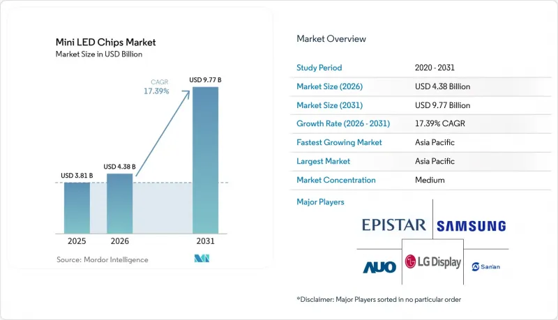
根據 Mordor Intelligence 預測,mini-LED 晶片市場規模將從 2025 年的 38.1 億美元和 2026 年的 43.8 億美元成長到 2031 年的 97.7 億美元,2026 年至 2031 年的年複合成長率(CAGR)為 17.39%。
本報告按晶片尺寸(100-200毫米和200-300毫米)、半導體材料(GaN/InGaN和AlGaInP)、應用(電視背光、遊戲顯示器和筆記型電腦、平板電腦和智慧型手機、汽車顯示器、VR/AR顯示器等)以及地區(北美、歐洲、亞太地區等)進行細分。市場預測以美元(USD)計價。
全球迷你LED晶片市場趨勢與洞察
高亮度HDR電視面板需求激增
在2026年的展會上,許多電視機亮相,它們擁有多達20000個局部調光區域,峰值亮度可達10000尼特,這在一定程度上削弱了發光技術在大螢幕電視領域的統治地位。中國品牌憑藉著積極的區域擴展和價格補貼優勢,在2026年初就佔據了全球電視出貨量的相當大佔有率。三星透過擴展其Neo QLED產品線並推出面向高亮度消費者的全新mini-LED產品,保持了其在美國市場的領先地位。面板製造商正在最佳化散熱設計和調光演算法,以在大螢幕大小上保持亮度。這項改變使得在不相應增加成本的情況下增加調光區域數量成為可能。隨著消費者越來越將亮度餘裕與畫質聯繫起來,mini-LED晶片市場在已開發市場和新興市場都受益於良性循環的升級。
先進的GaN-on-Si外延技術可提高晶圓良率
材料專家與大規模生產LED製造商之間的合作,正推動200mm矽基氮化鎵晶圓的商業化生產,在降低基板成本的同時,提高了每個製造週期內的晶片數量。晶格匹配的氮化鋁緩衝層的展示表明,外部量子效率提高了30%以上,這證明即使在矽基基板也能實現以前僅限於藍寶石基板的亮度目標。晶圓代工廠已為功率元件建立了成熟的工具集,這將減少額外的資本投入,並為向300mm晶圓的過渡鋪平道路,符合半導體行業的整體小型化藍圖。晶圓內部和晶圓之間均勻性的提高將提升良率,有助於面板製造商建立長期的成本降低路徑。這些優勢將強化垂直整合策略,並加速mini-LED晶片市場轉型為以矽為中心的供應鏈。
與OLED和新興的Micro-LED技術的競爭
蘋果將於2025年發表的iPad Pro將採用雙OLED面板,實現1000尼特的全螢幕亮度和200萬:1的對比度,這將削弱mini-LED在輕薄設備領域的優勢。 OLED價格的下降也影響了55吋和65吋電視市場,迫使mini-LED廠商增加分區數量和峰值亮度,以維持其高階定價。同時,針對200毫米晶圓的GaN-on-Si合作有望使micro-LED在未來實現成本持平,增加了預測期內技術逆轉的可能性。這兩方面的壓力正在縮短mini-LED維持高利潤率的時期,並減緩其在某些高階細分市場的成長預期。因此,廠商需要從亮度、壽命和螢幕大小等方面強化其價值提案,以保住市場佔有率。
細分市場分析
到2025年,100-200µm尺寸的LED晶片將佔據Mini LED晶片市場63.40%的佔有率,鞏固其在高分區電視和遊戲顯示器領域的地位。更小的晶片尺寸使電視製造商能夠在主流面板尺寸中整合更多局部調光區域,從而抑制光暈效應並保持具有競爭力的零售價格。由此產生的產量仍有利於藍寶石基板和成熟的大量生產流程。然而,面板買家對更高對比度的需求日益成長,促使供應商增加分區數量,這給檢測效率和良率管理帶來了壓力。晶片隔離和側壁鈍化技術的持續改進旨在保持更小尺寸晶片的亮度,確保該尺寸範圍的晶片在2031年之前保持主導地位。
預計200-300µm尺寸的LED晶片市場將以20.56%的複合年成長率成長,推動更大尺寸Mini LED晶片的市場規模擴大,因為汽車製造商和超大尺寸電視廠商正在簡化驅動架構。減少每個區域的晶片數量並提高單一晶片的亮度可以縮短實現時間,減少驅動器數量,並簡化曲面駕駛座顯示器(從A柱延伸到B柱)的散熱設計。此外,更大尺寸晶片的較低電流密度為汽車製造商提供了更大的餘地來滿足能源效率法規的要求。因此,供應商正在投資GaN-on-Si生產線,以平衡晶片數量的減少和晶片在玻璃上的鍵合精度,這種權衡確保了更大尺寸的晶片在超過1平方米的顯示區域仍然具有優勢。結合成本、可靠性和整合性優勢,預計到預測期結束時,該尺寸範圍的晶片與主流尺寸晶片的銷售差距將縮小。
區域分析
到2025年,亞太地區將佔全球mini-LED晶片銷售額的60.76%,預計到2031年將以21.54%的複合年成長率成長。這主要得益於中國政府補助、台灣外延技術以及韓國面板投資的共同作用,形成了一個自我強化的供應鏈網路。來自各省的津貼降低了新建晶圓廠的資本成本,而深圳和廈門等叢集則加速了大規模轉移和驅動IC封裝的學習週期。台灣向200mm氮化鎵矽基外延技術的轉型,充分利用了現有的半導體基礎設施,在不相應增加資本投入的情況下提高了產量。韓國主要顯示器製造商透過推廣其RGB mini-LED電視產品線,鞏固其在高階液晶顯示器領域的差異化優勢,同時擴大OLED晶圓廠的規模,從而維持了其市場佔有率。
北美地區的產量雖然較低,但憑藉高階遊戲顯示器和採用超大背光技術的優質電視,銷量卻十分亮眼。三星、宏碁和優派等品牌憑藉支持HDR1000以上標準的電視和顯示器,成功吸引了發燒友的目光。零售分析顯示,消費者傾向於選擇Mini-LED,因為它能提供OLED無法達到的峰值亮度,尤其是在郊區大型客廳等需要白天觀看的場所。汽車產業也為該地區的市場結構提供了支撐,底特律和矽谷的新創公司採用了專為美國資訊娛樂系統量身打造的曲面駕駛座面板,但這些面板仍然來自亞洲工廠。監管方面的阻力相對較小,但《通膨控制法案》下的製造業稅額扣抵可能會鼓勵驅動板和最終模組的本地組裝,從而有可能將部分供應轉移到美國。
儘管歐洲的市場佔有率不大,但它正透過推廣節能的生態設計法規來塑造技術發展方向。德國豪華汽車品牌正在採用mini-LED燈叢集和車內顯示螢幕,以滿足在明亮環境光下的可視性標準,這促使它們與台灣和日本的模組製造商建立合作關係。歐洲零售商正在推廣mini-LED電視,將其作為永續的升級選擇,因為與被取代的等離子電視相比,mini-LED電視每尼特亮度下的功耗更低。然而,不斷上漲的電價正在抑制顯示器的整體更換週期,導致其銷售成長速度低於亞太地區。 mini-LED在醫療影像和廣播工作室等工業應用領域的潛力,正為市場開闢新的成長途徑,充分利用其穩定的亮度和長壽命。
其他福利:
- Excel格式的市場預測(ME)表
- 3個月的分析師支持
目錄
第1章:引言
- 研究假設和市場定義
- 調查範圍
第2章:調查方法
第3章執行摘要
第4章 市場狀況
- 市場概覽
- 市場促進因素
- 市場對高亮度HDR電視面板的需求正在激增。
- 快速降低質傳裝置的成本
- 遊戲顯示器廠商更傾向於使用長壽命背光燈
- 推動制定節能型汽車駕駛座顯示器的相關法規
- 先進的GaN-on-Si外延技術可提高晶圓良率
- 區域補貼正加速中國Mini LED產能的擴張。
- 市場限制因素
- 潔淨室黏合線的高資本密集度
- 與OLED和新興的Micro-LED技術的競爭
- 藍寶石和稀土元素磷光體供應鏈的波動性
- 高密度LED陣列中複雜的溫度控管要求
- 產業供應鏈分析
- 宏觀經濟因素對市場的影響
- 監理情勢
- 技術展望
- 波特五力分析
第5章 市場規模與成長預測
- 按尖端尺寸
- 100~200µm
- 200~300µm
- 透過半導體材料
- GaN/InGaN
- AlGaInP
- 透過使用
- 電視背光
- 遊戲顯示器和筆記型電腦
- 平板電腦和智慧型手機
- 汽車顯示器(儀錶板、抬頭顯示器、資訊娛樂系統)
- VR/AR顯示器
- 其他應用(工業顯示器、醫療顯示器)
- 按地區
- 北美洲
- 歐洲
- 亞太地區
- 南美洲
- 中東和非洲
第6章 競爭情勢
- 市場集中度
- 策略趨勢
- 市佔率分析
- 公司簡介
- Epistar Corporation
- Samsung Electronics Co. Ltd.
- LG Display Co. Ltd.
- AUO Corporation
- San'an Optoelectronics Co. Ltd.
- Nichia Corporation
- Seoul Semiconductor Co. Ltd.
- Osram Opto Semiconductors GmbH
- Cree LED Inc.
- Lumileds Holding BV
- PlayNitride Inc.
- Lextar Electronics Corp.
- Innolux Corporation
- TCL Technology Group Corp.
- Vuereal Inc.
- Aledia SA
第7章 市場機會與未來展望
According to Mordor Intelligence, the mini lED chips market size is projected to expand from USD 3.81 billion in 2025 and USD 4.38 billion in 2026 to USD 9.77 billion by 2031, registering a CAGR of 17.39% between 2026 to 2031.
This report is Segmented by Chip Size (100-200 Mm and 200-300 Mm), Semiconductor Material (GaN/InGaN and AlGaInP), Application (Television Backlighting, Gaming Monitors and Laptops, Tablets and Smartphones, Automotive Displays, VR/AR Displays, and More), and Geography (North America, Europe, Asia Pacific, and More). The Market Forecasts are Provided in Terms of Value (USD).
Global Mini LED Chips Market Trends and Insights
Surging Demand for High-Brightness HDR Television Panels
Trade-show floors in 2026 were crowded with televisions boasting up to 20,000 local-dimming zones and 10,000 nits peak brightness, narrowing the perceived advantage of emissive technologies at premium screen sizes. Chinese brands captured a significant share of global TV unit shipments by early 2026 after pairing aggressive zone counts with subsidy-supported pricing. Samsung retained the top revenue position in the United States by expanding its Neo QLED range and adding new mini-LED SKUs that target brightness-oriented consumers. Panel makers are optimizing thermal architectures and dimming algorithms to sustain brightness across larger diagonals, a shift that amplifies zone counts without proportional cost jumps. As consumers equate luminance headroom with picture quality, the mini LED chips market benefits from a virtuous upgrade cycle across both developed and emerging regions.
Advanced GaN-on-Si Epitaxy Enabling Larger Wafer Yields
Partnerships between materials specialists and high-volume LED manufacturers are bringing 200 mm GaN-on-silicon wafers into commercial production, reducing substrate costs while increasing die counts per run. Demonstrations of lattice-compatible AlN buffer layers delivered external quantum-efficiency gains of more than 30%, validating that silicon substrates can meet brightness targets formerly reserved for sapphire. Foundry-style tool sets already in place for power devices lower incremental capex, creating a glide-path to 300 mm adoption that aligns with broader semiconductor scaling roadmaps. Higher on-wafer and wafer-to-wafer uniformity improves bin-yield economics, helping panel makers lock in long-term cost reduction trajectories. These advantages reinforce vertical integration plays and accelerate the migration of the mini LED chips market toward silicon-centric supply chains.
Competition from OLED and Emerging Micro-LED Technologies
Apple's 2025 iPad Pro launch showed tandem OLED panels hitting 1,000 nits full-screen brightness and a 2,000,000:1 contrast ratio, capabilities that erode mini-LED's advantage in thin-and-light devices. OLED price erosion is cascading into the 55-inch and 65-inch television tiers, forcing mini-LED brands to escalate zone counts and peak luminance just to sustain premiums. Meanwhile, GaN-on-Si partnerships targeting 200 mm wafers position micro-LED for future cost parity, raising the prospect of technological leapfrog within the forecast window. This two-front squeeze shortens the window during which mini-LED can command higher margins, tempering growth expectations in certain premium segments. Vendors must therefore sharpen value propositions around brightness, lifetime, and screen size to defend share.
Other drivers and restraints analyzed in the detailed report include:
- Regional Subsidies Accelerating Mini LED Capacity Build-Out in China
- Rapid Cost Decline in Mass-Transfer Equipment
- High Capital Intensity of Clean-Room Bonding Lines
For complete list of drivers and restraints, kindly check the Table Of Contents.
Segment Analysis
The 100-200 µm category captured 63.40% of the Mini LED Chips market share in 2025, cementing its role in high-zone televisions and gaming monitors. Smaller dice let set makers pack more local-dimming zones into mainstream panel sizes, suppressing halo artifacts while preserving aggressive retail price points. The resulting volumes anchor unit economics that still favor sapphire substrates and proven mass-transfer jigs. Yet panel buyers are signaling appetite for even richer contrast, nudging suppliers toward higher zone counts that strain inspection throughput and yield management. Continuous refinements in die singulation and sidewall passivation aim to sustain brightness at ever-smaller footprints, protecting the mainstream role of this size class through 2031.
The 200-300 µm group is projected to expand at a 20.56% CAGR, lifting the Mini LED Chips market size for larger chip formats as automakers and ultra-large TV vendors simplify driver architectures.Fewer, brighter dice per zone cut placement reduces placement time and driver count, easing thermal design for curved cockpit displays that stretch pillar to pillar. Automotive original equipment manufacturers also gain compliance headroom under energy-efficiency mandates because larger dice operate at lower current density. Suppliers therefore invest in GaN-on-Si lines that balance die-count reduction with chip-on-glass bonding precision, a trade-off that continues to favor larger dice in display areas above 1 m2. The convergence of cost, reliability, and integration advantages positions this size class to narrow the volume gap with mainstream formats by the end of the forecast window.
Geography Analysis
Asia Pacific accounted for 60.76% of mini LED chip revenue in 2025, and the region is forecast to grow at a 21.54% CAGR through 2031 as Chinese subsidies, Taiwanese epitaxy expertise, and Korean panel investments converge into a self-reinforcing supply network. Provincial grants lower capital costs for new fabs, while Shenzhen and Xiamen clusters shorten learning cycles on mass transfer and driver IC packaging. Taiwan's move to 200 mm GaN-on-silicon epitaxy leverages existing semiconductor infrastructure, raising output without proportional tool spend. Korea's display majors defend share by pushing RGB mini-LED TV lineups, anchoring premium LCD differentiation even as they scale OLED fabs.
North America contributes a smaller volume but outsized revenue thanks to high-end gaming monitors and premium televisions that favor mega-zone backlights. Brands such as Samsung, Acer, and ViewSonic capture enthusiast demand with sets and displays certified to HDR1000 and above. Retail analytics show consumers choosing mini-LED for peak brightness that OLED cannot sustain during daytime viewing, especially in large suburban living rooms. Automotive rollouts support the regional mix as Detroit and Silicon Valley startups adopt curved cockpit panels sourced from Asian fabs yet tuned to U.S. infotainment stacks. Regulatory headwinds are mild, but the Inflation Reduction Act's manufacturing credits could spur localized assembly of driver boards and final modules, nudging partial supply migration stateside.
Europe accounts for a modest share but sets technology direction through ecodesign regulations that push energy efficiency. German premium-car brands deploy mini-LED clusters and passenger displays to meet readability standards under bright ambient light, catalyzing partnerships with Taiwanese and Japanese module makers. European retailers promote mini-LED televisions as sustainable upgrades, citing lower power consumption per nit compared to plasma sets being replaced. However, elevated electricity prices temper overall screen-upgrade cycles, moderating unit growth compared with Asia Pacific. Industrial adoption in medical imaging and broadcast studios offers an incremental avenue, leveraging mini-LED's stable luminance and long lifetime.
- Epistar Corporation
- Samsung Electronics Co. Ltd.
- LG Display Co. Ltd.
- AUO Corporation
- San'an Optoelectronics Co. Ltd.
- Nichia Corporation
- Seoul Semiconductor Co. Ltd.
- Osram Opto Semiconductors GmbH
- Cree LED Inc.
- Lumileds Holding B.V.
- PlayNitride Inc.
- Lextar Electronics Corp.
- Innolux Corporation
- TCL Technology Group Corp.
- Vuereal Inc.
- Aledia S.A.
Additional Benefits:
- The market estimate (ME) sheet in Excel format
- 3 months of analyst support
TABLE OF CONTENTS
1 INTRODUCTION
- 1.1 Study Assumptions and Market Definition
- 1.2 Scope of the Study
2 RESEARCH METHODOLOGY
3 EXECUTIVE SUMMARY
4 MARKET LANDSCAPE
- 4.1 Market Overview
- 4.2 Market Drivers
- 4.2.1 Surging Demand for High-Brightness HDR Television Panels
- 4.2.2 Rapid Cost Decline in Mass-Transfer Equipment
- 4.2.3 OEM Preference for Longer-Lifetime Backlights in Gaming Monitors
- 4.2.4 Regulatory Push for Energy-Efficient Automotive Cockpit Displays
- 4.2.5 Advanced GaN-on-Si Epitaxy Enabling Larger Wafer Yields
- 4.2.6 Regional Subsidies Accelerating Mini LED Capacity Build-Out in China
- 4.3 Market Restraints
- 4.3.1 High Capital Intensity of Clean-Room Bonding Lines
- 4.3.2 Competition from OLED and Emerging Micro-LED Technologies
- 4.3.3 Supply-Chain Volatility for Sapphire and Rare-Earth Phosphors
- 4.3.4 Complex Thermal Management Requirements for Dense LED Arrays
- 4.4 Industry Supply-Chain Analysis
- 4.5 Impact of Macroeconomic Factors on the Market
- 4.6 Regulatory Landscape
- 4.7 Technological Outlook
- 4.8 Porter's Five Forces Analysis
- 4.8.1 Threat of New Entrants
- 4.8.2 Bargaining Power of Suppliers
- 4.8.3 Bargaining Power of Buyers
- 4.8.4 Threat of Substitutes
- 4.8.5 Competitive Rivalry
5 MARKET SIZE AND GROWTH FORECASTS (VALUE)
- 5.1 By Chip Size
- 5.1.1 100-200 µm
- 5.1.2 200-300 µm
- 5.2 By Semiconductor Material
- 5.2.1 GaN / InGaN
- 5.2.2 AlGaInP
- 5.3 By Application
- 5.3.1 Television Backlighting
- 5.3.2 Gaming Monitors and Laptops
- 5.3.3 Tablets and Smartphones
- 5.3.4 Automotive Displays (Instrument Cluster, HUD, Infotainment)
- 5.3.5 VR/AR Displays
- 5.3.6 Other Applications (Industrial Displays, Medical Displays)
- 5.4 By Geography
- 5.4.1 North America
- 5.4.2 Europe
- 5.4.3 Asia Pacific
- 5.4.4 South America
- 5.4.5 Middle East and Africa
6 COMPETITIVE LANDSCAPE
- 6.1 Market Concentration
- 6.2 Strategic Moves
- 6.3 Market Share Analysis
- 6.4 Company Profiles (includes Global Level Overview, Market Level Overview, Core Segments, Financials as available, Strategic Information, Market Rank/Share, Products and Services, Recent Developments)
- 6.4.1 Epistar Corporation
- 6.4.2 Samsung Electronics Co. Ltd.
- 6.4.3 LG Display Co. Ltd.
- 6.4.4 AUO Corporation
- 6.4.5 San'an Optoelectronics Co. Ltd.
- 6.4.6 Nichia Corporation
- 6.4.7 Seoul Semiconductor Co. Ltd.
- 6.4.8 Osram Opto Semiconductors GmbH
- 6.4.9 Cree LED Inc.
- 6.4.10 Lumileds Holding B.V.
- 6.4.11 PlayNitride Inc.
- 6.4.12 Lextar Electronics Corp.
- 6.4.13 Innolux Corporation
- 6.4.14 TCL Technology Group Corp.
- 6.4.15 Vuereal Inc.
- 6.4.16 Aledia S.A.
7 MARKET OPPORTUNITIES AND FUTURE OUTLOOK
- 7.1 White-Space and Unmet-Need Assessment
 日本LED晶片市場:市佔率分析、產業趨勢與統計及成長預測(2026-2031年)歐洲LED晶片:市佔率分析、產業趨勢與統計及成長預測(2026-2031年)中國LED晶片市場:市場佔有率分析、產業趨勢與統計及成長預測(2026-2031年)亞太地區LED晶片:市佔率分析、產業趨勢與統計及成長預測(2026-2031年)LED晶片:市場佔有率分析、產業趨勢與統計、成長預測(2026-2031年)北美LED晶片市場:市佔率分析、產業趨勢與統計及成長預測(2026-2031年)美國LED晶片:市佔率分析、產業趨勢與統計、成長預測(2026-2031年)
 LED晶片市場規模、佔有率、趨勢和預測:按產品、應用和地區分類,2026-2034年
 LED晶片市場分析及預測(至2035年):依類型、產品類型、技術、應用、材料類型、組件、最終用戶、設備、安裝類型分類
 LED晶片市場-全球產業規模、佔有率、趨勢、機會、預測:按應用、類型、最終用戶、地區和競爭格局分類,2021-2031年