


 |
市場調查報告書
商品編碼
2098541
AI加速器記憶體:市場佔有率分析、產業趨勢與統計資料、成長預測(2026-2031年)AI Accelerator Memory - Market Share Analysis, Industry Trends & Statistics, Growth Forecasts (2026 - 2031) |
||||||

※ 本網頁內容可能與最新版本有所差異。詳細情況請與我們聯繫。
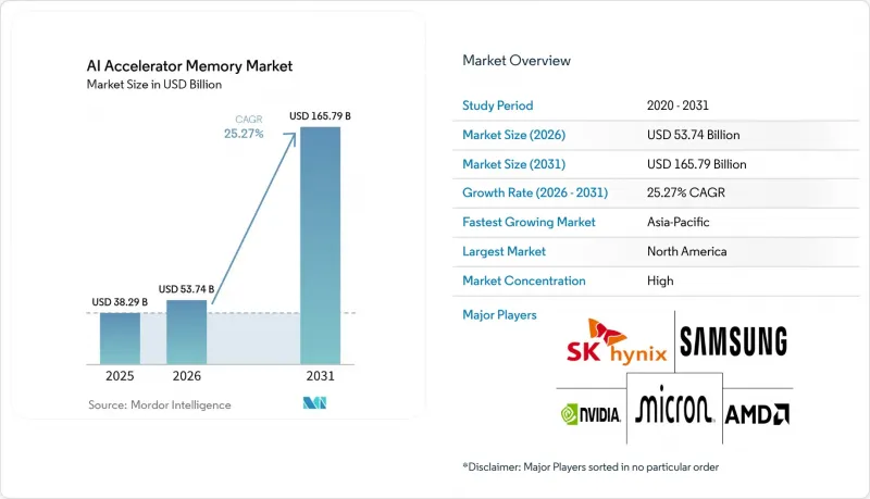
根據 Mordor Intelligence 預測,人工智慧加速器記憶體市場規模將從 2025 年的 382.9 億美元成長到 2026 年的 537.4 億美元,然後在 2031 年達到 1,657.9 億美元,2026 年至 2031 年的複合年成長率為 25.27%。
本報告按記憶體架構(HBM 等)、加速器平台(資料中心 GPU 加速器等)、HBM 代數(HBM2 和 HBM2E 等)、HBM 堆疊高度(最高 4 層等)、每個 HBM 堆疊的容量(最高 8 GB 等)、部署平台(超大規模雲和 AI 工廠等)以及地區進行細分。市場預測以美元 (USD) 為單位。
全球人工智慧加速器記憶體市場趨勢與洞察
在人工智慧加速器中擴大 HBM3E 和 HBM4 的應用
AI加速器記憶體市場受益於每一代HBM升級,因為效能的提升伴隨著更複雜的製造流程和更高的售價。 SK海力士宣布其HBM3E單腳傳輸速度高達9.6 Gbps,頻寬超過1.23 TB/s,符合AI加速器向更高密度和更快記憶體配置發展的趨勢。 2026年2月,三星宣布已開始採用其1c DRAM製程和4nm邏輯晶片量產HBM4,顯示市場已開始進入下一輪認證週期。 2026年6月,NVIDIA確認三星、SK海力士和美光均已獲得其Vera Rubin平台的認證並開始量產。這降低了供應商準備的不確定性,並擴大了下一代加速器量產的供應基礎。因此,AI 加速器記憶體市場正在擴張,不僅是因為單位需求增加,還因為每次向 HBM4 和 HBM4E 過渡都與更複雜、更昂貴的製造流程相關,從而導致收入增加。
人工智慧訓練和推理中計算密度的增加
AI加速器記憶體市場的發展也受到訓練和推理所需的單晶片記憶體容量和頻寬不斷成長的推動。 2026年4月,Google發布了TPU 8i,單晶片配備288GB HBM顯存,頻寬高達8601GB/s,同時片上SRAM容量也提升了三倍,達到384MB,這充分展現了內存需求在一個產品週期內的巨大成長。 NVIDIA的Vera Rubin平台進一步推動了這一趨勢,每個加速器採用576GB HBM4配置,顯示長上下文模型和大規模工作集持續推高最低記憶體需求。 JEDEC的LPDDR6藍圖也表明,記憶體功能正朝著更高級的方向發展,包括支援記憶體內處理(PIM),即使在邊緣系統中也是如此,這反映出減少資料移動和提高本地推理效率的普遍需求。在AI加速器記憶體市場,這意味著即使模型效率不斷提高,每個加速器的記憶體容量也在不斷成長。這是因為更長的上下文視窗和更複雜的推理管道會持續消耗額外的頻寬和容量。
封裝層面的嚴格熱設計和良率限制。
人工智慧加速器記憶體市場面臨嚴峻的技術挑戰。隨著層數增加和邏輯晶片整合到基礎結構中,溫度控管難度加大。三星HBM4的量產以及業界不斷提高堆疊高度的趨勢表明,記憶體廠商正努力在滿足認證和可靠性要求的前提下,實現更高的密度。 JEDEC標準仍然至關重要,因為商業化取決於每一代產品是否能達到既定的散熱和性能閾值。美光和Marvell都強調了對記憶體架構的改進,旨在減少資料傳輸和介面功耗,這表明挑戰不僅限於供應短缺,還延伸至封裝層面的可行性。因此,如果新的堆疊高度和新的邏輯製程相結合導致良率低於商業目標,人工智慧加速器記憶體市場將繼續面臨量產擴張速度低於預期的風險。
細分市場分析
預計到2025年,HBM將佔據AI加速器記憶體市場92.48%的佔有率,證實了主流AI加速器仍依賴極高的頻寬和高密度的封裝記憶體。谷歌的Ironwood TPU採用8個HBM3E堆疊,每個晶片的頻寬高達7370 GB/s;其後續產品TPU 8i的效能提升至8601 GB/s,每個晶片的容量為288 GB。這表明HBM仍然是最先進系統的預設設計選擇。 GDDR在低成本推理GPU和工作站卡中仍然佔據重要地位,系統設計人員仍需要在效能和整合成本之間取得平衡。 DDR對於混合AI伺服器中與CPU連接的功能也至關重要,尤其是在加速器與大型企業運算基礎架構一同部署的情況下。 AI加速器記憶體市場中HBM與其他架構配置之間的顯著差距反映了目前資料中心AI對頻寬加速器封裝的依賴程度。
LPDDR是成長最快的子細分市場,預計2026年至2031年複合年成長率將達到26.27%,這表明下一波需求浪潮將超越大型資料中心部署。 JEDEC宣布將在其LPDDR6藍圖中加入對「內存內處理(PIM)」的支持,從而將LPDDR的應用範圍擴展到資料中心和邊緣應用場景。這表明低功耗記憶體將在需要本地推理和低功耗的AI系統中發揮更大的作用。三星的LPDDR6計畫面向AI邊緣系統、AI PC、資料中心和汽車平台,這證實了供應商正在將LPDDR定位為AI記憶體的一個成長領域,而不僅僅是行動組件。美光也展示了LPDDR頻寬與邊緣AI中令牌產生速度的直接相關性,顯示即使在超大規模雲端之外,記憶體吞吐量也是一個直接的效能因素。因此,AI 加速器記憶體市場分為以資料中心為導向的 HBM 核心和以快速成長的邊緣運算的 LPDDR 層,每種架構都支援不同的部署模型。
2025年,資料中心GPU加速器佔據了AI加速器記憶體市場73.58%的佔有率,反映出主流訓練和推理GPU平台的強勁普及和廣泛應用。 NVIDIA的H100、H200和Blackwell系列繼續將GPU平台定位在大規模AI部署的核心,而AMD則透過即將推出的MI455X系列等平台,繼續保持其在HBM供應中的重要二級客戶地位。 AI SoC、NPU和APU繼續在行動、汽車和嵌入式AI領域得到應用,但它們的單位記憶體價值仍然低於大規模資料中心加速器。基於FPGA的加速器在對延遲敏感的工作負載中繼續發揮重要作用,在這些工作負載中,適應性和確定性回應時間仍然至關重要。這意味著,儘管其他平台類型擴大了需求基礎,但AI加速器記憶體市場仍由GPU主導的基礎設施所支撐。
預計到2031年,客製化AI ASIC和XPU的複合年成長率將達到26.46%,成為AI加速器記憶體市場中成長最快的平台細分領域。 2026年2月,博通宣布開始出貨其首款2nm客製化計算SoC,採用3.5D XDSiP架構,並支援多個HBM堆疊。這表明客製化晶片正以更快的速度向先進的異構封裝方向發展。 AWS Trainium、Google TPU 8和Meta MTIA 500等產品表明,超大規模超大規模資料中心業者擴大根據工作負載特定的頻寬和延遲目標來設計記憶體需求,而不是簡單地採用標準GPU模板。 Marvell的客製化HBM運算架構也增加了每個XPU的HBM堆疊數量,同時降低了介面功耗,使客製化記憶體介面成為客製化加速器極具競爭力的設計要素。隨著這一轉變的推進,與先前以 GPU 為主導的周期相比,AI 加速器記憶體市場在認證流程和產品特定的 HBM 配置方面將出現更大的差異。
區域分析
2025年,北美佔據了人工智慧加速器記憶體市場48.12%的佔有率,並持續保持著區域需求中心的地位。該地區的領先地位並非主要源於其記憶體製造能力,而是得益於超大規模企業的聚集、客製化晶片專案以及大規模人工智慧伺服器的部署。 2026年2月,亞馬遜決定在路易斯安那州投資120億美元,這充分展現了其對這項持續影響該地區硬體需求的單一項目的投入規模。谷歌也在2026年擴展了其TPU藍圖,進一步鞏固了北美作為記憶體密集型加速器早期採用者的重要地位。加拿大透過為資料中心提供有利的電力供應條件,為該地區的成長提供了支持;而墨西哥則作為建立未來人工智慧基礎設施的近岸中心,吸引了許多關注。
預計到2031年,亞太地區將以26.19%的複合年成長率成長,成為人工智慧加速器記憶體市場成長最快的地區。該地區既是先進HBM的製造地,也是人工智慧基礎設施需求的新興中心,扮演著雙重角色。韓國憑藉SK海力士和三星的晶圓廠網路保持其核心地位,而美光的廣島工廠也已成為更廣泛的太平洋供應鏈中的關鍵生產基地。 SK海力士位於龍仁的叢集計畫於2026年2月獲批,投資額達21.61兆韓元(約160億美元),顯示該地區正在對未來的記憶體產能進行大量投資。日本提供先進的封裝技術,而印度和東南亞則透過人工智慧雲端的擴展、人工智慧PC的普及以及本地推理系統的部署,持續擴大市場需求。
儘管歐洲、南美洲以及中東和非洲目前在人工智慧(AI)加速器記憶體市場中所佔小規模,但它們各自都對AI加速器記憶體市場產生了策略性需求。德國和英國引領了歐洲AI伺服器的普及,而「法國2030」等公共舉措也持續推動國內運算能力的提升。歐盟《人工智慧法案》進一步加速了區域基礎設施規劃,因為合規性和資料管理開始影響企業AI工作負載的部署地點。在中東和非洲,沙烏地阿拉伯和阿拉伯聯合大公國主導的AI叢集採購項目,以及出口框架和跨境技術協議的支持,提升了AI的重要性。南美仍處於引進週期的早期階段,但巴西和智利正在為未來區域AI基礎設施的擴展奠定基礎。
其他好處:
- Excel格式的市場預測(ME)表
- 3個月的分析師支持
目錄
第1章:引言
- 研究假設和市場定義
- 調查範圍
第2章:調查方法
第3章執行摘要
第4章 市場狀況
- 市場概覽
- 市場促進因素
- 在人工智慧加速器中擴大 HBM3E 和 HBM4 的應用
- 提高人工智慧訓練和推理的計算密度
- 在超大規模資料中心擴展人工智慧基礎設施
- 提高最先進GPU和ASIC的每瓦頻寬需求
- 將供應重新分配至高利潤率的人工智慧記憶體SKU
- 晶片級人工智慧架構的廣泛應用
- 市場限制因素
- 封裝層面的熱性能和良率限制非常嚴格。
- 先進高密度脂蛋白(HBM)的供應基礎合格。
- 對先進包裝能力的高度依賴
- 出口限制和供應鏈本地化帶來的摩擦
- 產業價值鏈分析
- 監理情勢
- 技術展望
- 宏觀經濟因素對市場的影響
- 波特五力分析
第5章 市場規模與成長預測
- 依記憶體架構
- 高頻寬體(HBM)
- 雙倍資料速率記憶體用於圖形
- 低功耗雙數據速率記憶體
- 雙倍資料速率記憶體
- 其他專用加速內存
- 透過加速器平台
- 用於資料中心的GPU加速器
- 客製化人工智慧專用積體電路和擴充處理器
- AI SoC、NPU、APU
- 基於FPGA的加速器
- 資料處理單元、智慧網路卡與網路加速器
- 其他加速器平台
- 按世代分類的 HBM
- HBM2 和 HBM2E
- HBM3
- HBM3E
- HBM4
- HBM4E 和下一代 HBM
- 按高度排列的 HBM 堆疊
- 少於 4 級
- 8個步驟
- 12步
- 16步
- 16步或更多
- 每個 HBM 堆疊的容量
- 小於 8 GB
- 8 GB~16 GB
- 16 GB~24 GB
- 24 GB~36 GB
- 36 GB 或更多
- 透過部署平台
- 超大規模雲端和人工智慧工廠
- 企業及本地資料中心
- 高效能運算和研究系統
- 網路和通訊基礎設施
- 邊緣人工智慧和工業系統
- AI工作站和AI個人電腦
- 汽車人工智慧和自動駕駛系統
- 按地區
- 北美洲
- 美國
- 加拿大
- 墨西哥
- 歐洲
- 德國
- 英國
- 法國
- 義大利
- 其他歐洲國家
- 亞太地區
- 中國
- 日本
- 韓國
- 印度
- 東南亞
- 其他亞太國家
- 南美洲
- 中東和非洲
- 北美洲
第6章 競爭情勢
- 市場集中度
- 策略趨勢
- 市場定位分析
- 公司簡介
- SK hynix Inc.
- Samsung Electronics Co., Ltd.
- Micron Technology, Inc.
- NVIDIA Corporation
- Advanced Micro Devices, Inc.
- Intel Corporation
- Taiwan Semiconductor Manufacturing Company Limited
- ASML Holding NV
- Applied Materials, Inc.
- Lam Research Corporation
- KLA Corporation
- Tokyo Electron Limited
- Amkor Technology, Inc.
- ASE Technology Holding Co., Ltd.
- JCET Group Co., Ltd.
- Powertech Technology Inc.
- Tongfu Microelectronics Co., Ltd.
- Marvell Technology, Inc.
- Synopsys, Inc.
- Cadence Design Systems, Inc.
第7章 市場機會與未來展望
According to Mordor Intelligence, the AI accelerator memory market size is expected to grow from USD 38.29 billion in 2025 to USD 53.74 billion in 2026 and is forecast to reach USD 165.79 billion by 2031 at 25.27% CAGR over 2026-2031.
This report is Segmented by Memory Architecture (HBM, and More), Accelerator Platform (Data Center GPU Accelerators, and More), HBM Generation (HBM2 and HBM2E, and More), HBM Stack Height (Up To 4-High, and More), HBM Capacity Per Stack (Up To 8 GB, and More), Deployment Platform (Hyperscale Cloud and AI Factories, and More), and Geography. The Market Forecasts are Provided in Terms of Value (USD).
Global AI Accelerator Memory Market Trends and Insights
Growing Adoption of HBM3E and HBM4 in AI Accelerators
The AI accelerator memory market is benefiting from each HBM generation upgrade because higher performance now comes with greater process complexity and higher selling prices. SK hynix stated that its HBM3E reached up to 9.6 Gbps per pin and more than 1.23 TB/s of bandwidth, underscoring why current AI accelerators continue to move toward denser, faster memory configurations. Samsung said in February 2026 that it had begun mass production of HBM4 using a 1c DRAM process and a 4 nm logic base die, signaling that the market had already begun shifting to the next qualification cycle. NVIDIA confirmed in June 2026 that Samsung, SK hynix, and Micron had all qualified and entered production for its Vera Rubin platform, reducing uncertainty around vendor readiness and widening the supply base for the next accelerator ramp. The AI accelerator memory market, therefore, moves higher not only because unit demand is rising, but also because each transition to HBM4 and HBM4E ties revenue growth to a more demanding and more expensive manufacturing path.
Rising AI Training and Inference Compute Density
The AI accelerator memory market is also being pushed by the steady rise in memory capacity and bandwidth required per chip for both training and inference. Google introduced TPU 8i in April 2026 with 288 GB of HBM and 8,601 GB/s per chip, while also tripling on-chip SRAM to 384 MB, demonstrating how memory intensity has risen in one product cycle. NVIDIA's Vera Rubin platform extended that direction with a 576 GB HBM4 configuration per accelerator, indicating that long-context models and larger working sets are still pushing minimum memory requirements upward. JEDEC's LPDDR6 roadmap also showed that even edge systems are moving toward richer memory functions, including processing-in-memory support, which reflects broader pressure to reduce data movement and improve local inference efficiency. In the AI accelerator memory market, this means memory content per accelerator is rising even when model efficiency improves, because longer context windows and more complex inference pipelines continue to consume additional bandwidth and capacity.
High Package-Level Thermal and Yield Constraints
The AI accelerator memory market faces a significant technical constraint; thermal management becomes more difficult as layer counts rise and logic dies are integrated into the base structure. Samsung's HBM4 ramp and the industry's move to higher stack heights show that memory vendors are trying to increase density while staying within qualification and reliability limits. JEDEC standards remain important because commercialization depends on meeting defined thermal and performance thresholds across successive generations. Micron and Marvell both highlighted memory architecture changes aimed at reducing data movement and interface power, confirming that the issue is not limited to raw supply volume but extends to package-level feasibility. This keeps the artificial intelligence (AI) accelerator memory market vulnerable to slower-than-expected ramps whenever new stack heights or new logic-process combinations push yields below commercial targets.
Other drivers and restraints analyzed in the detailed report include:
- Expansion of Hyperscale Data Center AI Fleets
- Higher Bandwidth Demand Per Watt in Advanced GPUs and ASICs
- Limited Qualified Supply Base for Advanced HBM
For complete list of drivers and restraints, kindly check the Table Of Contents.
Segment Analysis
HBM held 92.48% of the AI accelerator memory market share by memory architecture in 2025, which confirms that leading AI accelerators still depend on very high bandwidth and dense on-package memory. Google's Ironwood TPU deployed 8 stacks of HBM3E at 7,370 GB/s per chip, and the later TPU 8i lifted performance to 8,601 GB/s with 288 GB per chip, which shows why HBM stayed the default design choice for frontier systems. GDDR kept a role in lower-cost inference GPUs and workstation cards, where system designers still balance performance against integration cost. DDR also remained relevant for CPU-attached functions in hybrid AI servers, especially when accelerators are deployed alongside broader enterprise compute infrastructure. In the AI accelerator memory market, this wide gap between HBM and the rest of the architecture mix reflects how strongly current data center AI depends on bandwidth-intensive accelerator packages.
LPDDR is the fastest-growing sub-segment, with a 26.27% CAGR from 2026 to 2031, indicating that the next wave of demand is broadening beyond the largest data center deployments. JEDEC said its LPDDR6 roadmap adds processing-in-memory support and extends LPDDR into data centers and edge use cases, suggesting a wider role for low-power memory in AI systems that need local inference and lower energy draw. Samsung's LPDDR6 program targets AI edge systems, AI PCs, data centers, and automotive platforms, confirming that suppliers are treating LPDDR as an AI memory growth area rather than just a mobile component. Micron also linked LPDDR bandwidth directly to token-generation speed in edge AI, making memory throughput a direct performance lever outside the hyperscale cloud. The AI accelerator memory market is therefore splitting into a data center HBM core and a fast-growing edge LPDDR layer, with each architecture serving a distinct deployment model.
Data Center GPU Accelerators captured 73.58% of the AI accelerator memory market size in 2025, reflecting the installed base and allocation strength of mainstream training and inference GPU platforms. NVIDIA's H100, H200, and Blackwell families kept GPU platforms at the center of large-scale AI deployments, while AMD remained a meaningful secondary customer route for HBM supply through platforms such as MI455X in the next cycle. AI SoCs, NPUs, and APUs continued to serve mobile, automotive, and embedded AI, but their memory value per unit remained lower than that of large data center accelerators. FPGA-based accelerators still mattered in latency-sensitive workloads where adaptability and deterministic response times remained important. This left the AI accelerator memory market anchored by GPU-led infrastructure, even as other platform types widened the demand base.
Custom AI ASICs and XPUs are projected to grow at 26.46% CAGR through 2031, making them the fastest-growing platform segment in the AI accelerator memory market. Broadcom said in February 2026 that it began shipping the first 2 nm custom compute SoC on its 3.5D XDSiP architecture, with support for multiple HBM stacks, demonstrating how custom silicon is moving into advanced heterogeneous packaging earlier and faster. AWS Trainium, Google TPU 8, and Meta MTIA 500 indicate that hyperscalers are increasingly designing their memory needs around workload-specific bandwidth and latency targets rather than accepting a standard GPU template. Marvell's custom HBM compute architecture also supports more HBM stacks per XPU with lower interface power, which makes tailored memory interfaces a competitive design feature for custom accelerators. As that shift continues, the AI accelerator memory market will see a broader mix of qualification paths and product-specific HBM configurations than it did in the prior GPU-dominated cycle.
Complete Report Scope:
- By Memory Architecture
- High Bandwidth Memory (HBM)
- Graphics Double Data Rate Memory
- Low-Power Double Data Rate Memory
- Double Data Rate Memory
- Other Specialized Accelerator Memory
- By Accelerator Platform
- Data Center GPU Accelerators
- Custom AI ASICs and XPUs
- AI SoCs, NPUs, and APUs
- FPGA-Based Accelerators
- Data Processing Units, SmartNICs, and Networking Accelerators
- Other Accelerator Platforms
- By HBM Generation
- HBM2 and HBM2E
- HBM3
- HBM3E
- HBM4
- HBM4E and Next-Generation HBM
- By HBM Stack Height
- Up to 4-High
- 8-High
- 12-High
- 16-High
- Above 16-High
- By HBM Capacity per Stack
- Up to 8 GB
- 8 GB to 16 GB
- 16 GB to 24 GB
- 24 GB to 36 GB
- Above 36 GB
- By Deployment Platform
- Hyperscale Cloud and AI Factories
- Enterprise and On-Premise Data Centers
- High-Performance Computing and Research Systems
- Networking and Telecommunications Infrastructure
- Edge AI and Industrial Systems
- AI Workstations and AI PCs
- Automotive AI and Autonomous Systems
- By Geography
- North America
- United States
- Canada
- Mexico
- Europe
- Germany
- United Kingdom
- France
- Italy
- Rest of Europe
- Asia-Pacific
- China
- Japan
- South Korea
- India
- Southeast Asia
- Rest of Asia-Pacific
- South America
- Middle East and Africa
- North America
Geography Analysis
North America held 48.12% of the AI accelerator memory market in 2025, maintaining its position as the leading regional demand center. The region's lead came from the concentration of hyperscale buyers, custom silicon programs, and large AI server deployments rather than from memory manufacturing capacity alone. Amazon's February 2026 decision to invest USD 12 billion in Louisiana showed the scale of single-project commitments that continue to shape regional hardware demand. Google also expanded its TPU roadmap in 2026, reinforcing North America's role as the primary early-deployment zone for memory-intensive accelerators. Canada supported regional growth through favorable power conditions for data centers, while Mexico gained attention as a nearshore infrastructure corridor for future AI buildouts.
Asia-Pacific is projected to grow at 26.19% CAGR through 2031, making it the fastest-growing region in the AI accelerator memory market. The region plays a dual role as both the manufacturing base for advanced HBM and a rising center of demand for AI infrastructure. South Korea remained central through the fab networks of SK hynix and Samsung, while Micron's Hiroshima site added an important production node in the broader Pacific supply chain. SK hynix's KRW 21.61 trillion (approximately USD 16 billion) Yongin cluster approval in February 2026 showed how heavily the region is investing in future memory output. Japan contributed advanced packaging capabilities, and India and Southeast Asia continued to build demand through AI cloud expansion, AI PC adoption, and local inference deployments.
Europe, South America, the Middle East, and Africa remained smaller in current share, but each added strategic demand for the artificial intelligence (AI) accelerator memory market. Germany and the United Kingdom led European AI server deployments, while public initiatives such as France 2030 continued supporting domestic compute capacity. The EU AI Act also encouraged more local infrastructure planning because compliance and data control now influence where enterprise AI workloads are hosted. The Middle East and Africa gained importance through sovereign AI cluster procurement in Saudi Arabia and the UAE, supported by export frameworks and cross-border technology agreements. South America remained earlier in its cycle, but Brazil and Chile continued laying the groundwork for future regional AI infrastructure expansion.
- SK hynix Inc.
- Samsung Electronics Co., Ltd.
- Micron Technology, Inc.
- NVIDIA Corporation
- Advanced Micro Devices, Inc.
- Intel Corporation
- Taiwan Semiconductor Manufacturing Company Limited
- ASML Holding N.V.
- Applied Materials, Inc.
- Lam Research Corporation
- KLA Corporation
- Tokyo Electron Limited
- Amkor Technology, Inc.
- ASE Technology Holding Co., Ltd.
- JCET Group Co., Ltd.
- Powertech Technology Inc.
- Tongfu Microelectronics Co., Ltd.
- Marvell Technology, Inc.
- Synopsys, Inc.
- Cadence Design Systems, Inc.
Additional Benefits:
- The market estimate (ME) sheet in Excel format
- 3 months of analyst support
TABLE OF CONTENTS
1 INTRODUCTION
- 1.1 Study Assumptions and Market Definition
- 1.2 Scope of the Study
2 RESEARCH METHODOLOGY
3 EXECUTIVE SUMMARY
4 MARKET LANDSCAPE
- 4.1 Market Overview
- 4.2 Market Drivers
- 4.2.1 Growing Adoption of HBM3E and HBM4 in AI Accelerators
- 4.2.2 Rising AI Training and Inference Compute Density
- 4.2.3 Expansion of Hyperscale Data Center AI Fleets
- 4.2.4 Higher Bandwidth Demand per Watt in Advanced GPUs and ASICs
- 4.2.5 Supply Reallocation Toward High-Margin AI Memory SKUs
- 4.2.6 Rising Adoption of Chiplet-Based AI Architectures
- 4.3 Market Restraints
- 4.3.1 High Package-Level Thermal and Yield Constraints
- 4.3.2 Limited Qualified Supply Base for Advanced HBM
- 4.3.3 Heavy Dependence on Advanced Packaging Capacity
- 4.3.4 Export Controls and Supply Chain Localization Friction
- 4.4 Industry Value Chain Analysis
- 4.5 Regulatory Landscape
- 4.6 Technological Outlook
- 4.7 Impact of Macroeconomic Factors on the Market
- 4.8 Porter's Five Forces Analysis
- 4.8.1 Bargaining Power of Suppliers
- 4.8.2 Bargaining Power of Buyers
- 4.8.3 Threat of New Entrants
- 4.8.4 Threat of Substitutes
- 4.8.5 Intensity of Competitive Rivalry
5 MARKET SIZE AND GROWTH FORECASTS (VALUE)
- 5.1 By Memory Architecture
- 5.1.1 High Bandwidth Memory (HBM)
- 5.1.2 Graphics Double Data Rate Memory
- 5.1.3 Low-Power Double Data Rate Memory
- 5.1.4 Double Data Rate Memory
- 5.1.5 Other Specialized Accelerator Memory
- 5.2 By Accelerator Platform
- 5.2.1 Data Center GPU Accelerators
- 5.2.2 Custom AI ASICs and XPUs
- 5.2.3 AI SoCs, NPUs, and APUs
- 5.2.4 FPGA-Based Accelerators
- 5.2.5 Data Processing Units, SmartNICs, and Networking Accelerators
- 5.2.6 Other Accelerator Platforms
- 5.3 By HBM Generation
- 5.3.1 HBM2 and HBM2E
- 5.3.2 HBM3
- 5.3.3 HBM3E
- 5.3.4 HBM4
- 5.3.5 HBM4E and Next-Generation HBM
- 5.4 By HBM Stack Height
- 5.4.1 Up to 4-High
- 5.4.2 8-High
- 5.4.3 12-High
- 5.4.4 16-High
- 5.4.5 Above 16-High
- 5.5 By HBM Capacity per Stack
- 5.5.1 Up to 8 GB
- 5.5.2 8 GB to 16 GB
- 5.5.3 16 GB to 24 GB
- 5.5.4 24 GB to 36 GB
- 5.5.5 Above 36 GB
- 5.6 By Deployment Platform
- 5.6.1 Hyperscale Cloud and AI Factories
- 5.6.2 Enterprise and On-Premise Data Centers
- 5.6.3 High-Performance Computing and Research Systems
- 5.6.4 Networking and Telecommunications Infrastructure
- 5.6.5 Edge AI and Industrial Systems
- 5.6.6 AI Workstations and AI PCs
- 5.6.7 Automotive AI and Autonomous Systems
- 5.7 By Geography
- 5.7.1 North America
- 5.7.1.1 United States
- 5.7.1.2 Canada
- 5.7.1.3 Mexico
- 5.7.2 Europe
- 5.7.2.1 Germany
- 5.7.2.2 United Kingdom
- 5.7.2.3 France
- 5.7.2.4 Italy
- 5.7.2.5 Rest of Europe
- 5.7.3 Asia-Pacific
- 5.7.3.1 China
- 5.7.3.2 Japan
- 5.7.3.3 South Korea
- 5.7.3.4 India
- 5.7.3.5 Southeast Asia
- 5.7.3.6 Rest of Asia-Pacific
- 5.7.4 South America
- 5.7.5 Middle East and Africa
- 5.7.1 North America
6 COMPETITIVE LANDSCAPE
- 6.1 Market Concentration
- 6.2 Strategic Moves
- 6.3 Market Positioning Analysis
- 6.4 Company Profiles (includes Global Level Overview, Market Level Overview, Core Segments, Financials as available, Strategic Information, Market Rank/Share, Products and Services, Recent Developments)
- 6.4.1 SK hynix Inc.
- 6.4.2 Samsung Electronics Co., Ltd.
- 6.4.3 Micron Technology, Inc.
- 6.4.4 NVIDIA Corporation
- 6.4.5 Advanced Micro Devices, Inc.
- 6.4.6 Intel Corporation
- 6.4.7 Taiwan Semiconductor Manufacturing Company Limited
- 6.4.8 ASML Holding N.V.
- 6.4.9 Applied Materials, Inc.
- 6.4.10 Lam Research Corporation
- 6.4.11 KLA Corporation
- 6.4.12 Tokyo Electron Limited
- 6.4.13 Amkor Technology, Inc.
- 6.4.14 ASE Technology Holding Co., Ltd.
- 6.4.15 JCET Group Co., Ltd.
- 6.4.16 Powertech Technology Inc.
- 6.4.17 Tongfu Microelectronics Co., Ltd.
- 6.4.18 Marvell Technology, Inc.
- 6.4.19 Synopsys, Inc.
- 6.4.20 Cadence Design Systems, Inc.
7 MARKET OPPORTUNITIES AND FUTURE OUTLOOK
- 7.1 White-Space and Unmet-Need Assessment

 802.11ac Wave 2 市場規模、佔有率和成長分析:按組件、設備類型、頻段、最終用戶、應用、分銷管道和地區分類 - 行業預測,2026-2033 年
 日本快閃記憶體市場:市場佔有率分析、產業趨勢與統計及成長預測(2026-2031)
 軍用級保護殼市場分析與預測(至2035年):類型、產品、服務、技術、應用、材料類型、部署、最終用戶、功能、安裝配置
 人工智慧蓬勃發展與DRAM供不應求:全球DRAM市場展望(2027年)人工智慧記憶體:市場佔有率分析、產業趨勢與統計、成長預測(2026-2031)汽車產業NOR快閃記憶體:市場佔有率分析、產業趨勢與統計及成長預測(2026-2031年)高速LPDDR5X DRAM:市場佔有率分析、產業趨勢與統計數據、成長預測(2026-2031年)德國 NOR Flush:市場佔有率分析、行業趨勢和統計數據、成長預測(2026-2031 年)東南亞NOR快閃記憶體:市場佔有率分析、產業趨勢與統計、成長預測(2026-2031年)NOR Flush(英國):市場佔有率分析、行業趨勢和統計數據、成長預測(2026-2031 年)