


 |
市場調查報告書
商品編碼
2072558
美國NOR快閃記憶體:市場佔有率分析、產業趨勢與統計資料、成長預測(2026-2031年)United States NOR Flash - Market Share Analysis, Industry Trends & Statistics, Growth Forecasts (2026 - 2031) |
||||||
※ 本網頁內容可能與最新版本有所差異。詳細情況請與我們聯繫。
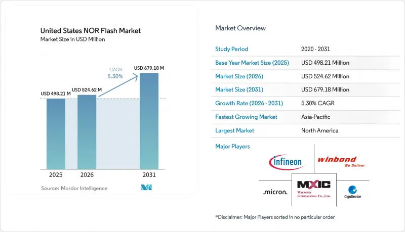
據 Mordor Intelligence 稱,2025 年美國 NOR 快閃記憶體市值為 4.9821 億美元,預計到 2031 年將達到 6.7918 億美元,而 2026 年為 5.2462 億美元,預測期(2026-2031 年)的複合年成長率為 5.3%。
本報告按類型(串行和平行)、密度(2兆位元及以下和以上)、電壓(3V級、1.8V級以上)、最終用戶應用(家用電子電器、電信設備、汽車等)、製程節點(65奈米、55奈米等)和封裝類型(WLCSP/CSP等)進行細分。市場預測以價值(美元)和數量(單位)表示。
美國NOR快閃記憶體市場的趨勢與洞察
美國對ADAS和功能安全ECU中高可靠性NOR的需求激增。
部署 L2+ 和 L3 級自動駕駛技術的汽車製造商現在要求使用符合 ISO 26262 ASIL-D 標準的快閃記憶體。英飛凌的「Semper」系列快閃記憶體已獲得此認證,使一級供應商能夠在保證確定性啟動的同時減少冗餘層數。在區域架構中,眾多小型 ECU 整合到高效能控制器中,每個區域的快閃記憶體密度需求已增加到 128 Mb 至 512 Mb。特斯拉在德克薩斯州生產的 AI5 平台採用外部串行 NOR 快閃記憶體來隔離安全關鍵韌體,其多年供貨合約已延長至 2029 年車型。這些因素共同表明,串行 NOR 閃存在電動車產能擴張的關鍵路徑上佔據重要地位。
晶片法和科學法獎勵加速了國內NOR晶片的生產
截至2025年7月,《晶片與科學法案》已向40個項目撥款共364億美元。其中四分之三的項目集中在亞利桑那州、紐約州和德克薩斯州,旨在汽車和國防工業中心附近建立記憶體製造廠。區域補貼正在縮小與亞洲生產的成本差距,而安靠公司位於皮奧裡亞的WLCSP生產線則為汽車製造商提供符合ITAR規定的封裝方案。儘管晶圓新創公司數量預計在2028年之前不會大幅成長,但客戶已經開始下達「照付不議」的訂單以確保未來的產能,這表明他們對國內供應鏈充滿信心。
SPI-NAND快閃記憶體製程(超過28奈米節點)的製造成本很高。
採用 28nm 製程的 SPI-NAND 在 1Gb 密度下成本約為每兆位元組 0.015 美元,相比成本高於每兆位元組 0.05 美元的 NOR 快閃記憶體而言,成本優勢更為顯著。如此巨大的成本差異正促使對成本敏感的 OEM 廠商轉向 SPI-NAND,尤其是在啟動延遲並非關鍵因素的應用中。代工廠越來越重視高利潤邏輯產品的生產,導致 NOR 快閃記憶體只能在老舊的生產設備上使用。這些老舊設備缺乏 NAND 快閃記憶體所具備的規模經濟優勢,進一步拉大了成本差距。因此,NOR 快閃記憶體技術難以保持成本效益和競爭力,尤其是在高密度應用中。
細分市場分析
到2025年,串行NOR快閃記憶體將佔據美國NOR快閃記憶體市場60.9%的佔有率。隨著汽車OEM廠商用4埠和8埠裝置取代笨重的並行元件以縮小基板尺寸,串列NOR快閃記憶體的領先優勢將進一步擴大。這一趨勢使得供應商能夠以更高的利潤率提升銷售安全啟動功能,從而鞏固了美國NOR快閃記憶體市場。並行NOR快閃記憶體仍應用於國防抗輻射加固設計和傳統工業控制器中,在這些應用中,15年的性能保證比太空限制更為重要。因此,供應商將兩種介面都作為雙介面產品提供,但出貨量成長和產品藍圖投資顯然更傾向於串列產品,儘管美國NOR快閃記憶體市場整體擴張,並行產品的銷售卻停滯不前。
第二代串列產品提供 400 MB/s 的原地執行速度和 AES-256 加密,使基於區域的 ECU 能夠直接載入 Linux 鏡像,而無需經過 DRAM。隨著 RISC-V MCU 的普及,新創公司因其廣泛的工具鏈支援而選擇串行 NOR,這增強了生態系統效應,並進一步邊緣化了並行 NOR。因此,串行 NOR 正在成為汽車製造商、工業IoT和 5G 基礎設施的戰略基石,而並行 NOR 仍然是傳統市場的收入來源。
到2025年,四路SPI將佔總銷售額的46.2%,而八路和xSPI的成長速度更快,複合年成長率達10.6%。這一成長主要得益於對集中式汽車控制器日益成長的需求,這些控制器需要400 MB/s的頻寬才能有效載入冗餘韌體映像。隨著設計人員將速度和確定性讀取置於每位元成本之上,這種轉變正在擴大美國NOR快閃記憶體市場的高利潤細分領域。單路和雙路SPI正逐步被推向注重成本的消費市場,而四路SPI仍是中階標準。另一方面,八路SPI憑藉其卓越的性能,正逐漸成為高階選擇。
八路 SPI 裝置現在整合了以前僅在平行總線上才有的高級功能,例如差分訊號和 ECC。 JEDEC xSPI 2.0 規範進一步提高了吞吐量,使其接近 PCIe Gen2 的水平,同時保持了低引腳封裝的優勢。這項進步顯著縮小了曾經足以證明並行介面優勢的效能差距。隨著 OEM 廠商重新設計 2028 年款的控制單元,xSPI 的普及預計將會加速。這一趨勢將鞏固 xSPI 作為高可靠性應用領先啟動標準的地位,並進一步擴大其市場佔有率。
儘管預計到2025年128MB容量的快閃記憶體仍將保持28.7%的市場佔有率,但由於基於Linux的資訊娛樂系統和ADAS感測器融合技術的應用,對更大韌體分區的需求正在成長,推動市場向256MB至1GB的容量方向發展。這種向更高密度的轉變正在擴大美國NOR快閃記憶體的市場規模,因為平均售價的上漲抵消了更大晶片尺寸帶來的劣勢。另一方面,低容量產品,尤其是低於8MB的產品,正在萎縮,因為整合到微控制器中的MRAM使得低於64MB的記憶體容量不再需要外部程式碼儲存。這一趨勢凸顯了高階應用中對高容量解決方案日益成長的需求。
為了在不依賴新型微影術技術的情況下實現Gigabit級容量,供應商將兩個 512 Mb 晶片堆疊在單一 BGA 或 WLCSP 封裝內。這種方法既能繼續使用成熟的 55 奈米工藝,又能滿足汽車認證標準,從而確保其在汽車應用中的可靠性。此外,此策略還能有效防止嵌入式對低階市場的侵蝕。因此,市場正經歷著由密度而非容量成長驅動的轉變,預計到 2031 年,以密度主導的產品架構變革將成為主要的收入來源。
其他好處:
- Excel格式的市場預測(ME)表
- 3個月的分析師支持
目錄
第1章:引言
- 研究假設和市場定義
- 調查範圍
第2章:調查方法
第3章執行摘要
第4章 市場狀況
- 市場概覽
- 產業價值鏈分析
- 市場促進因素
- 美國ADAS和功能安全ECU對高可靠性NOR記憶體的需求激增。
- 5G毫米波基地台的快速部署正在推動對NOR碼儲存的需求。
- 美國國防部航太和國防領域的現代化需要耐輻射的NOR(天然導向回收材料)
- 在美國惡劣環境下部署工業IoT,需要即時啟動記憶體。
- 《晶片與科學法案》下的優惠待遇正在加速國內天然口腔精煉 (NOR) 的生產。
- 新興的開放原始碼RISC-V MCU 生態系統實現了外部 NOR 記憶體的標準化,從而實現安全啟動。
- 市場限制因素
- 28nm節點之後SPI-NAND的製造成本很高。
- 在微控制器中採用嵌入式MRAM和RRAM作為替代代碼儲存設備
- 國內缺乏 300mm 製造能力限制了高密度 NOR 底片的供應。
- 關鍵製程氣體(氖氣、氟氣)供應的波動加劇了成本的不確定性。
- 宏觀經濟因素對市場的影響
- 監管和技術展望
- 波特五力分析
- 價格分析
- 投資分析
第5章 市場規模與成長預測
- 按類型
- 串行 NOR 快閃記憶體
- 並行 NOR 快閃記憶體
- By Interface
- SPI 單/雙路
- 四路 SPI
- 八進位和xSPI
- 按密度
- 2兆位元或以下的NOR閘
- 4兆位元(超過2兆位元)NOR
- 8兆位元(超過4兆位元)NOR
- 16兆位元(超過8兆位元)NOR
- 32兆位元(超過16兆位元)NOR
- 64兆位元(超過32兆位元)NOR
- 128兆位元(64兆位元或以上)NOR
- 256兆位元(128兆位元或以上)NOR
- 超過 256 兆比特
- 透過電壓
- 3 V級
- 1.8 V級
- 寬電壓範圍(1.65V 至 3.6V)
- 低於 1.8 V 的類別(1.2 V、2.5 V、5 V)
- 透過最終用戶應用程式
- 家用電子產品
- 溝通
- 車
- 產業
- 其他終端用戶應用程式
- 依製程技術節點
- 90奈米及更早
- 65 nm
- 55 nm
- 45 nm
- 28奈米或更小
- 按包裝類型
- WLCSP/CSP
- QFN/SOIC
- BGA/FBGA
- 其他包裝類型
第6章 競爭情勢
- 市場集中度
- 策略趨勢
- Vendor Positioning Analysis
- 公司簡介
- Infineon Technologies AG
- Micron Technology Inc.
- Winbond Electronics Corporation
- Macronix International Co. Ltd.
- GigaDevice Semiconductor Inc.
- Renesas Electronics Corporation
- Integrated Silicon Solution Inc.
- Microchip Technology Inc.
- Elite Semiconductor Microelectronics Technology Inc.
- Puya Semiconductor(Shanghai)Co. Ltd.
- Alliance Memory Inc.
- STMicroelectronics NV
- Samsung Semiconductor
- SkyHigh Memory Limited
- Etron Technology Inc.
- AMIC Technology Corp.
- Cypress Semiconductor Corp.
- Teledyne e2v Semiconductors
- Fudan Microelectronics Group Co. Ltd.
- Silicon Storage Technology Inc.
第7章 市場機會與未來展望
According to Mordor Intelligence, the united states NOR flash market size was valued at USD 498.21 million in 2025 and is estimated to grow from USD 524.62 million in 2026 to reach USD 679.18 million by 2031, at a CAGR of 5.3% during the forecast period (2026-2031).
This report is Segmented by Type (Serial, and Parallel), Density (2 Megabit and Less NOR, and More), Voltage (3V Class, 1. 8V Class, and More), End-User Application (Consumer Electronics, Communication Equipment, Automotive and More), Process Technology Node (65 Nm, 55 Nm, and More), and Packaging Type (WLCSP/CSP, and More). The Market Forecasts are Provided in Terms of Value (USD) and Volume (Units).
United States NOR Flash Market Trends and Insights
Surge in Demand for High-Reliability NOR in U.S. ADAS and Functional-Safety ECUs
Automakers that are rolling out Level 2+ and Level 3 autonomy now require flash that meets ISO 26262 ASIL-D. Infineon's Semper family attained that certificate, enabling Tier 1s to reduce redundancy layers while still guaranteeing deterministic boot. Zonal architectures consolidate many small ECUs into high-performance controllers, lifting density needs to 128 Mb-512 Mb per zone. Tesla's AI5 platform produced in Texas relies on external serial NOR to isolate safety-critical firmware, and multiyear supply contracts already stretch to the 2029 model year. These factors collectively place serial NOR on the critical path of EV production ramps.
CHIPS and Science Act Incentives Accelerating Domestic NOR Manufacturing
Through July 2025, CHIPS disbursed USD 36.4 billion across 40 projects, three-quarters of which reside in Arizona, New York, and Texas, anchoring memory-capable fabs near automotive and defense clusters. Local subsidies narrow the cost gap with Asian production, and Amkor's Peoria WLCSP line gives automakers an ITAR-compliant packaging option. While wafer starts will not meaningfully add until 2028, customers are already placing take-or-pay orders that secure futures capacity, signaling confidence in a domestically sourced supply chain.
High Fabrication Cost Versus SPI-NAND Beyond 28-Nanometer Nodes
SPI-NAND achieves a cost of approximately USD 0.015 per Mb at a 1 Gb density on 28 nm technology, making it a more economical choice compared to NOR, which remains above USD 0.05 per Mb. This significant cost difference is prompting cost-sensitive OEMs to transition to SPI-NAND, especially in applications where boot latency is not a critical factor. Foundries are increasingly prioritizing high-margin logic production, leaving NOR confined to older manufacturing equipment. This older equipment lacks the scale-economy advantages that NAND benefits from, further widening the cost gap. As a result, NOR technology struggles to compete in terms of cost efficiency, particularly in high-density applications.
Other drivers and restraints analyzed in the detailed report include:
- Rapid Roll-Out of 5G mmWave Base-Stations Driving NOR Code-Storage Demand
- Industrial IoT Deployments in Harsh U.S. Environments Needing Instant-Boot Memory
- Limited Domestic 300-Millimeter Capacity Constraining High-Density NOR Supply
For complete list of drivers and restraints, kindly check the Table Of Contents.
Segment Analysis
Serial NOR Flash accounted for 60.9% of the United States NOR Flash market share in 2025, a lead that is widening as automotive OEMs replace bulky parallel devices with quad- and octal-variant devices to trim board size. The trend strengthens the United States NOR Flash market by allowing vendors to upsell secure-boot features at premium margins. Parallel NOR still services defense rad-hard designs and legacy industrial controllers where 15-year form-fit-function commitments override space constraints. Vendors therefore dual-source both interfaces, but volume growth and roadmap investment clearly favor serial parts, keeping parallel revenue flat even as the overall United States NOR Flash market size rises.
Second-generation serial parts offer execute-in-place at 400 MB/s and AES-256 encryption, enabling zonal ECUs to load Linux images directly without DRAM staging. As RISC-V MCUs proliferate, start-ups pick serial NOR for its broad tool-chain support, reinforcing an ecosystem effect that further marginalizes parallel. Consequently, serial NOR becomes the strategic linchpin for automakers, industrial IoT, and 5G infrastructure, while parallel NOR becomes a legacy-harvest play.
Quad SPI captured 46.2% of revenue in 2025, yet octal and xSPI are growing faster, with a 10.6% CAGR. This growth is driven by the increasing demand for centralized automotive controllers, which require 400 MB/s bandwidth to load redundant firmware images efficiently. The shift is expanding the high-margin segment of the United States NOR Flash market, as designers prioritize speed and deterministic reads over cost per bit. Single- and dual-SPI are gradually being relegated to cost-sensitive consumer segments, while quad-SPI remains the mid-range standard. Octal SPI, on the other hand, is emerging as the premium choice due to its superior performance capabilities.
Octal devices now incorporate advanced features such as differential signaling and ECC, which were previously exclusive to parallel buses. JEDEC's xSPI 2.0 specification has further enhanced throughput, bringing it closer to PCIe Gen2 levels while maintaining the benefits of low-pin-count packages. This development has significantly reduced the performance gap that once justified the use of parallel interfaces. As OEMs prepare to redesign control units for the 2028 model years, the adoption of xSPI is expected to accelerate. This trend positions xSPI as the leading boot standard for high-reliability applications, solidifying its market position.
The 128 Mb tier retained 28.7% share in 2025, but Linux-based infotainment stacks and ADAS sensor fusion are driving the need for larger firmware partitions, pushing demand toward 256 MB-1 GB capacities. This shift toward higher densities is boosting the United States NOR Flash market size, as the increase in average selling prices outweighs the penalties associated with larger die sizes. Meanwhile, lower-density parts, particularly those <=8 Mb, are witnessing a decline as embedded MRAM within microcontrollers eliminates the requirement for external code storage below 64 Mb. This trend highlights the growing preference for higher-density solutions in advanced applications.
To achieve gigabit capacities without relying on new lithography advancements, vendors are stacking two 512 Mb dies within a single BGA or WLCSP package. This approach allows mature 55 nm processes to remain relevant while preserving automotive qualification standards, which are critical for maintaining reliability in automotive applications. Additionally, this strategy serves as a safeguard against the erosion of low-end sockets by embedded alternatives. As a result, the market is experiencing a shift driven by density rather than unit growth, positioning density-driven mix shifts as the primary revenue driver through 2031.
Complete Report Scope:
- By Type (Value, Volume)
- Serial NOR Flash
- Parallel NOR Flash
- By Interface (Value)
- SPI Single / Dual
- Quad SPI
- Octal and xSPI
- By Density (Value)
- 2 Megabit and Less NOR
- 4 Megabit (More than 2 Mb) NOR
- 8 Megabit (More than 4 Mb) NOR
- 16 Megabit (More than 8 Mb) NOR
- 32 Megabit (More than 16 Mb) NOR
- 64 Megabit (More than 32 Mb) NOR
- 128 Megabit (More than 64 Mb) NOR
- 256 Megabit (More than 128 Mb) NOR
- Greater than 256 Megabit
- By Voltage (Value)
- 3 V Class
- 1.8 V Class
- Wide-Voltage (1.65 V - 3.6 V)
- Sub-1.8 V Classes (1.2 V, 2.5 V, 5 V)
- By End-User Application (Value, Volume)
- Consumer Electronics
- Communication
- Automotive
- Industrial
- Other End-User Applications
- By Process Technology Node (Value)
- 90 nm and Older
- 65 nm
- 55 nm
- 45 nm
- 28 nm and Below
- By Packaging Type (Value)
- WLCSP / CSP
- QFN / SOIC
- BGA / FBGA
- Other Packaging Types
List of Companies Covered in this Report:
- Infineon Technologies AG
- Micron Technology Inc.
- Winbond Electronics Corporation
- Macronix International Co. Ltd.
- GigaDevice Semiconductor Inc.
- Renesas Electronics Corporation
- Integrated Silicon Solution Inc.
- Microchip Technology Inc.
- Elite Semiconductor Microelectronics Technology Inc.
- Puya Semiconductor (Shanghai) Co. Ltd.
- Alliance Memory Inc.
- STMicroelectronics NV
- Samsung Semiconductor
- SkyHigh Memory Limited
- Etron Technology Inc.
- AMIC Technology Corp.
- Cypress Semiconductor Corp.
- Teledyne e2v Semiconductors
- Fudan Microelectronics Group Co. Ltd.
- Silicon Storage Technology Inc.
Additional Benefits:
- The market estimate (ME) sheet in Excel format
- 3 months of analyst support
TABLE OF CONTENTS
1 INTRODUCTION
- 1.1 Study Assumptions and Market Definition
- 1.2 Scope of the Study
2 RESEARCH METHODOLOGY
3 EXECUTIVE SUMMARY
4 MARKET LANDSCAPE
- 4.1 Market Overview
- 4.2 Industry Value-Chain Analysis
- 4.3 Market Drivers
- 4.3.1 Surge in Demand for High-Reliability NOR in U.S. ADAS and Functional-Safety ECUs
- 4.3.2 Rapid Roll-Out of 5G mmWave Base-Stations Driving NOR Code-Storage Demand
- 4.3.3 DoD Aerospace and Defense Modernization Requiring Radiation-Tolerant NOR
- 4.3.4 Industrial IoT Deployments in Harsh U.S. Environments Needing Instant-Boot Memory
- 4.3.5 CHIPS and Science Act Incentives Accelerating Domestic NOR Manufacturing
- 4.3.6 Emerging Open-Source RISC-V MCU Ecosystem Standardizing on External NOR for Secure Boot
- 4.4 Market Restraints
- 4.4.1 High Fabrication Cost Versus SPI-NAND Beyond 28 nm Nodes
- 4.4.2 Adoption of Embedded MRAM and RRAM as Alternative Code Storage in MCUs
- 4.4.3 Limited Domestic 300 mm Capacity Constraining High-Density NOR Supply
- 4.4.4 Volatility in Critical Process Gas Supply (Neon, Fluorine) Raising Cost Unpredictability
- 4.5 Impact of Macroeconomic Factors on the Market
- 4.6 Regulatory and Technological Outlook
- 4.7 Porter's Five Forces Analysis
- 4.7.1 Bargaining Power of Suppliers
- 4.7.2 Bargaining Power of Buyers
- 4.7.3 Threat of New Entrants
- 4.7.4 Threat of Substitute Products
- 4.7.5 Intensity of Competitive Rivalry
- 4.8 Pricing Analysis
- 4.9 Investment Analysis
5 MARKET SIZE AND GROWTH FORECASTS (VALUE, VOLUME)
- 5.1 By Type (Value, Volume)
- 5.1.1 Serial NOR Flash
- 5.1.2 Parallel NOR Flash
- 5.2 By Interface (Value)
- 5.2.1 SPI Single / Dual
- 5.2.2 Quad SPI
- 5.2.3 Octal and xSPI
- 5.3 By Density (Value)
- 5.3.1 2 Megabit and Less NOR
- 5.3.2 4 Megabit (More than 2 Mb) NOR
- 5.3.3 8 Megabit (More than 4 Mb) NOR
- 5.3.4 16 Megabit (More than 8 Mb) NOR
- 5.3.5 32 Megabit (More than 16 Mb) NOR
- 5.3.6 64 Megabit (More than 32 Mb) NOR
- 5.3.7 128 Megabit (More than 64 Mb) NOR
- 5.3.8 256 Megabit (More than 128 Mb) NOR
- 5.3.9 Greater than 256 Megabit
- 5.4 By Voltage (Value)
- 5.4.1 3 V Class
- 5.4.2 1.8 V Class
- 5.4.3 Wide-Voltage (1.65 V - 3.6 V)
- 5.4.4 Sub-1.8 V Classes (1.2 V, 2.5 V, 5 V)
- 5.5 By End-User Application (Value, Volume)
- 5.5.1 Consumer Electronics
- 5.5.2 Communication
- 5.5.3 Automotive
- 5.5.4 Industrial
- 5.5.5 Other End-User Applications
- 5.6 By Process Technology Node (Value)
- 5.6.1 90 nm and Older
- 5.6.2 65 nm
- 5.6.3 55 nm
- 5.6.4 45 nm
- 5.6.5 28 nm and Below
- 5.7 By Packaging Type (Value)
- 5.7.1 WLCSP / CSP
- 5.7.2 QFN / SOIC
- 5.7.3 BGA / FBGA
- 5.7.4 Other Packaging Types
6 COMPETITIVE LANDSCAPE
- 6.1 Market Concentration
- 6.2 Strategic Moves
- 6.3 Vendor Positioning Analysis
- 6.4 Company Profiles
- 6.4.1 Infineon Technologies AG
- 6.4.2 Micron Technology Inc.
- 6.4.3 Winbond Electronics Corporation
- 6.4.4 Macronix International Co. Ltd.
- 6.4.5 GigaDevice Semiconductor Inc.
- 6.4.6 Renesas Electronics Corporation
- 6.4.7 Integrated Silicon Solution Inc.
- 6.4.8 Microchip Technology Inc.
- 6.4.9 Elite Semiconductor Microelectronics Technology Inc.
- 6.4.10 Puya Semiconductor (Shanghai) Co. Ltd.
- 6.4.11 Alliance Memory Inc.
- 6.4.12 STMicroelectronics NV
- 6.4.13 Samsung Semiconductor
- 6.4.14 SkyHigh Memory Limited
- 6.4.15 Etron Technology Inc.
- 6.4.16 AMIC Technology Corp.
- 6.4.17 Cypress Semiconductor Corp.
- 6.4.18 Teledyne e2v Semiconductors
- 6.4.19 Fudan Microelectronics Group Co. Ltd.
- 6.4.20 Silicon Storage Technology Inc.
7 MARKET OPPORTUNITIES AND FUTURE OUTLOOK
- 7.1 White-space and Unmet-need Assessment
 德國 NOR Flush:市場佔有率分析、行業趨勢和統計數據、成長預測(2026-2031 年)東南亞NOR快閃記憶體:市場佔有率分析、產業趨勢與統計、成長預測(2026-2031年)NOR Flush(英國):市場佔有率分析、行業趨勢和統計數據、成長預測(2026-2031 年)亞太地區NOR快閃記憶體:市場佔有率分析、產業趨勢與統計、成長預測(2026-2031年)
 2026年全球金屬氧化物半導體(MOS)微處理器市場報告2026年全球金屬氧化物半導體(MOS)標準單元和現場可程式邏輯市場報告印度NOR沖洗液:市場佔有率分析、產業趨勢與統計、成長預測(2026-2031年)歐洲NOR快閃記憶體:市場佔有率分析、產業趨勢與統計、成長預測(2026-2031年)NOR閃存在家用電子電器)。工業級NOR快閃記憶體:市場佔有率分析、產業趨勢與統計、成長預測(2026-2031年)