

 |
市場調查報告書
商品編碼
2125643
日本半導體裝置:市場佔有率分析、產業趨勢與統計、成長預測(2026-2031)Japan Semiconductor Device - Market Share Analysis, Industry Trends & Statistics, Growth Forecasts (2026 - 2031) |
||||||

※ 本網頁內容可能與最新版本有所差異。詳細情況請與我們聯繫。
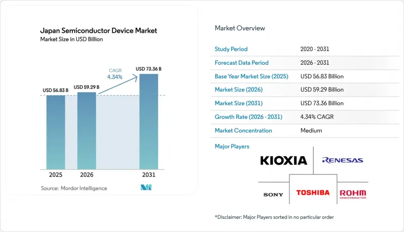
據估計,日本半導體裝置市場規模從2025年的568.3億美元成長到2026年的592.9億美元,預計到2031年將達到733.6億美元。
預計 2026 年至 2031 年的複合年成長率為 4.34%。
本報告按元件類型(離散半導體、光電子元件、感測器和微機電系統、積體電路)、經營模式(整合元件製造商和設計/無晶圓廠供應商)以及終端用戶產業(汽車、電信、消費性電子、工業、運算/資料儲存、資料中心、人工智慧、政府等)進行細分。市場預測以美元計價。
日本半導體裝置市場的趨勢與洞察
電動車動力傳動系統需求激增
在電動車架構中,多種機械部件正被固態子系統所取代,從而推動了對牽引逆變器、車用充電器和ADAS控制器的需求。國內領導者正在採用d模GaN開關,其在中壓範圍內表現優於SiC,這不僅擴大了目標市場,也保持了定價權。一級供應商與裝置製造商之間的策略合作正在加速設計採納週期,使日本半導體裝置市場能夠受益於每輛車矽使用量的增加。強制性的碳排放減排目標正在鞏固本地採購協議,而健全的汽車生態系統正在加速認證進程,這表明中期內對功率元件的需求將趨於穩定。
5G/6G基礎設施的穩健部署
日本不斷成長的中頻寬密度以及6G預標準化測試平台的建立,推動了吞吐量和延遲指標的提升,而這些指標無法透過傳統矽晶片滿足。日本國內射頻專家透過將GaN HEMT與自主研發的匹配網路相結合,突破了基地台的熱極限,鞏固了市場佔有率並確保了高利潤率。等電漿蝕刻和MOCVD設備供應的本地化進一步降低了生產風險,來自海外無廠半導體公司的訂單也源源不斷地湧入日本半導體裝置市場叢集。這些因素對網路測試設備產生了連鎖反應,拓展了下游市場的機遇,並確保了需求的持續成長。
先進微影術領域長期存在人員短缺問題
EUV設備的引進需要精通2nm及以下製程整合的工程師,但國內人才培育體系每年僅能培養出數十名畢業生。跨國公司以兩位數的薪資溢價吸引經驗豐富的海外人才,進一步加劇了國內人才短缺的情況。儘管獎學金計畫和中年員工的再培訓在一定程度上緩解了這個問題,但產能擴張計畫仍然依賴引進外國工程師,這增加了學習曲線延長和良率提升延遲的風險。這可能會影響日本半導體裝置市場的短期成長動能。
細分市場分析
到2025年,積體電路(IC)將佔日本半導體裝置市場銷售額的85.62%,這主要得益於客製化人工智慧加速器、汽車SoC和多層3D NAND快閃記憶體的推動。邊緣推理ASIC晶片消耗著最先進的晶圓,而高層NAND快閃記憶體封裝則佔據了雲端儲存的機架,為生產提供了獨立但互補的支援。感測器和微機電系統(MEMS)正以5.59%的複合年成長率成長,儘管規模較小,但這主要歸功於ADAS雷達帶來的更多應用點以及工廠車間的維修。在光電子領域,日本正利用其在雷射雷達和AR頭顯用雷射二極體的全球領先地位。分離式功率元件的成長較為溫和,但碳化矽MOSFET和氮化鎵電晶體的平均售價(ASP)不斷提高,從而穩定了利潤率。
從節點層面觀點,其獨特之處在於兩條發展路徑並行推進。 7奈米以下製程的生產線支援人工智慧和高效能運算,而成熟的40-65奈米製程則服務於汽車電子和工業控制設備。這種雙軌製程結構使日本半導體裝置市場不受經濟週期波動的影響,滿足市場需求,並支援均衡的晶圓廠運營,避免過度依賴特定客戶領域。諸如千層3D NAND等技術突破,鞏固了日本在國內高密度製造領域的領先地位,並增強了其出口競爭力。
其他好處:
- Excel格式的市場預測(ME)表
- 3個月的分析師支持
目錄
第1章:引言
- 研究假設和市場定義
- 調查範圍
第2章:調查方法
第3章執行摘要
第4章 市場狀況
- 市場概覽
- 市場促進因素
- 電動車動力傳動系統需求激增
- 部署強大的 5G/6G 基礎設施
- 政府對先進節點製造的補貼
- 智慧家庭消費物聯網的普及
- 日本在垂直GaN/SiC研發領域的領先地位
- 為確保供應鏈安全而採取的回流激勵措施
- 市場限制因素
- 先進微影術領域長期存在人員短缺問題
- 與特種氣體和化學品相關的供應鏈風險
- 地震可能導致運作停產
- 小於 28 奈米製程節點的傳統設備已過時
- 產業價值鏈分析
- 監理情勢
- 技術展望
- 波特五力分析
- 宏觀經濟因素對市場的影響
第5章 市場規模與成長預測
- 依設備類型
- 法令半導體
- 二極體
- 電晶體
- 功率電晶體
- 整流器和閘流體
- 其他離散半導體
- 光電子學
- 發光二極體(LED)
- 雷射二極體
- 影像感測器
- 歐普託卡普拉
- 其他光電子裝置
- 感測器和微機電系統
- 壓力
- 磁場
- 執行器
- 加速度和偏航率
- 溫度感測器和其他感測器,MEMS
- 積體電路
- 依積體電路類型
- 模擬
- 微
- 微處理器(MPU)
- 微控制器(MCU)
- 數位訊號處理器
- 邏輯
- 記憶
- 依技術節點
- 小於3奈米
- 3 nm
- 5 nm
- 7 nm
- 16 nm
- 28 nm
- 28奈米或更大
- 依積體電路類型
- 法令半導體
- 按經營模式
- IDM
- 設計/無晶圓廠供應商
- 按最終用戶行業分類
- 車
- 通訊(有線和無線)
- 一般消費者
- 產業
- 計算/數據存儲
- 資料中心
- 人工智慧
- 政府(航太/國防)
- 其他終端用戶產業
第6章 競爭情勢
- 市場集中度
- 策略趨勢
- 市佔率分析
- 公司簡介
- Renesas Electronics Corporation
- Rohm Co., Ltd.
- Toshiba Electronic Devices and Storage Corporation
- Sony Semiconductor Solutions Corporation
- Kioxia Holdings Corporation
- Socionext Inc.
- Mitsubishi Electric Corporation
- Megachips Corporation
- Kyocera Corporation
- ABLIC Inc.
- Ricoh Electronic Devices Co., Ltd.
- Nisshinbo Micro Devices Inc.
- New Japan Radio Co., Ltd.
- Seiko Epson Corporation
- Seiko Instruments Inc.
- Sumitomo Electric Industries, Ltd.
- Hitachi Power Semiconductor Device, Ltd.
- Alps Alpine Co., Ltd.
- Sharp Corporation
- Fuji Electric Co., Ltd.
- Semiconductor Energy Laboratory Co., Ltd.
第7章 市場機會與未來展望
According to Mordor Intelligence, Japan semiconductor device market size in 2026 is estimated at USD 59.29 billion, growing from 2025 value of USD 56.83 billion with 2031 projections showing USD 73.36 billion, growing at 4.34% CAGR over 2026-2031.
This report is Segmented by Device Type (Discrete Semiconductors, Optoelectronics, Sensors and MEMS, and Integrated Circuits), Business Model (IDM and Design/Fabless Vendor), and End-User Industry (Automotive, Communication, Consumer, Industrial, Computing/Data Storage, Data Centre, Artificial Intelligence, Government, and More). The Market Forecasts are Provided in Terms of Value (USD).
Japan Semiconductor Device Market Trends and Insights
Electric-vehicle power-train demand surge
EV architectures replace multiple mechanical parts with solid-state subsystems, elevating demand for traction inverters, on-board chargers, and ADAS controllers. Domestic leaders deploy d-mode GaN switches that outperform SiC at mid-range voltages, broadening addressable markets while retaining pricing power. Strategic partnerships between tier-one suppliers and device makers accelerate design-win cycles, ensuring that the Japan semiconductor device market benefits from higher silicon content per vehicle. Mandatory carbon-reduction targets solidify local offtake agreements, and a deep automotive ecosystem supports rapid qualification, embedding power-device gains for the medium term.
Robust 5G/6G infrastructure roll-out
Japan's mid-band densification and pre-standard 6G testbeds push throughput and latency specifications that legacy silicon cannot satisfy. Domestic RF specialists combine GaN HEMTs with proprietary matching networks to hit base-station thermal limits, cementing share while capturing premium margins. Localization of plasma-etch and MOCVD tool supply further lowers production risk, drawing additional foreign fabless orders into the Japan semiconductor device market cluster. Spillovers into network-testing equipment widen downstream opportunities, guaranteeing sustained incremental demand.
Chronic talent shortage in advanced lithography
EUV tool installations require engineers versed in sub-2 nm process integration, yet the domestic pipeline adds only a few dozen graduates per year. Multinationals lure experienced staff overseas with double-digit wage premiums, widening local gaps. Although scholarship programs and mid-career retraining provide relief, ramp schedules still hinge on expatriate hires, stretching learning curves and raising risk of yield-ramp delays that could dent the Japan semiconductor device market's near-term growth trajectory.
Other drivers and restraints analyzed in the detailed report include:
- Government subsidies for advanced-node fabs
- Consumer IoT proliferation in smart homes
- Supply-chain exposure to specialty gases and chemicals
For complete list of drivers and restraints, kindly check the Table Of Contents.
Segment Analysis
Integrated Circuits generated 85.62% of Japan semiconductor device market revenue in 2025, sustained by bespoke AI accelerators, automotive SoCs, and multilayer 3D NAND. Edge-inference ASICs consume leading-edge wafers, while high-layer NAND packages fill cloud-storage racks, anchoring volume in separate but complementary streams. Sensors and MEMS, though smaller, expand at a 5.59% CAGR as ADAS radar and factory-floor retrofits multiply attach points. Optoelectronics leverages national leadership in laser diodes for LiDAR and AR headsets. Discrete power devices grow modestly, but SiC MOSFETs and GaN transistors earn richer ASPs, stabilizing contribution margins.
A node-level view highlights a dual-track approach: sub-7 nm lines support AI and high-performance computing, whereas mature 40-65 nm flows serve car electronics and industrial control. This split lets the Japan semiconductor device market capture demand across cycles, underwriting balanced fabs that avoid over-reliance on any single customer vertical. Breakthroughs such as 1,000-layer 3D NAND will keep density leadership in the domestic ecosystem, strengthening export competitiveness.
Complete Report Scope:
- By Device Type
- Discrete Semiconductors
- Diodes
- Transistors
- Power Transistors
- Rectifier and Thyristor
- Other Discrete Semiconductors
- Optoelectronics
- Light-Emitting Diodes (LEDs)
- Laser Diodes
- Image Sensors
- Optocouplers
- Other Optoelectronics
- Sensors and MEMS
- Pressure
- Magnetic Field
- Actuators
- Acceleration and Yaw Rate
- Temperature and Other Sensors and MEMS
- Integrated Circuits
- By IC Type
- Analog
- Micro
- Microprocessors (MPU)
- Microcontrollers (MCU)
- Digital Signal Processors
- Logic
- Memory
- By Technology Node
- less than 3 nm
- 3 nm
- 5 nm
- 7 nm
- 16 nm
- 28 nm
- Above 28 nm
- By IC Type
- Discrete Semiconductors
- By Business Model
- IDM
- Design/Fabless Vendor
- By End-user Industry
- Automotive
- Communication (Wired and Wireless)
- Consumer
- Industrial
- Computing/Data Storage
- Data Centre
- Artificial Intelligence
- Government (Aerospace and Defence)
- Other End-user Industry
List of Companies Covered in this Report:
- Renesas Electronics Corporation
- Rohm Co., Ltd.
- Toshiba Electronic Devices and Storage Corporation
- Sony Semiconductor Solutions Corporation
- Kioxia Holdings Corporation
- Socionext Inc.
- Mitsubishi Electric Corporation
- Megachips Corporation
- Kyocera Corporation
- ABLIC Inc.
- Ricoh Electronic Devices Co., Ltd.
- Nisshinbo Micro Devices Inc.
- New Japan Radio Co., Ltd.
- Seiko Epson Corporation
- Seiko Instruments Inc.
- Sumitomo Electric Industries, Ltd.
- Hitachi Power Semiconductor Device, Ltd.
- Alps Alpine Co., Ltd.
- Sharp Corporation
- Fuji Electric Co., Ltd.
- Semiconductor Energy Laboratory Co., Ltd.
Additional Benefits:
- The market estimate (ME) sheet in Excel format
- 3 months of analyst support
TABLE OF CONTENTS
1 INTRODUCTION
- 1.1 Study Assumptions and Market Definition
- 1.2 Scope of the Study
2 RESEARCH METHODOLOGY
3 EXECUTIVE SUMMARY
4 MARKET LANDSCAPE
- 4.1 Market Overview
- 4.2 Market Drivers
- 4.2.1 Electric-Vehicle (EV) Power-Train Demand Surge
- 4.2.2 Robust 5G/6G Infrastructure Roll-Out
- 4.2.3 Government Subsidies for Advanced-Node Fabs
- 4.2.4 Consumer IoT Proliferation in Smart Homes
- 4.2.5 Vertical GaN/SiC RandD Leadership in Japan
- 4.2.6 Reshoring Incentives for Secure Supply Chains
- 4.3 Market Restraints
- 4.3.1 Chronic Talent Shortage in Advanced Lithography
- 4.3.2 Supply-Chain Exposure to Specialty Gases and Chemicals
- 4.3.3 Earthquake-Induced Downtime Risk for Fabs
- 4.3.4 Legacy Equipment Obsolescence for Sub-28 Nm Nodes
- 4.4 Industry Value Chain Analysis
- 4.5 Regulatory Landscape
- 4.6 Technological Outlook
- 4.7 Porter's Five Forces Analysis
- 4.7.1 Bargaining Power of Suppliers
- 4.7.2 Bargaining Power of Buyers
- 4.7.3 Threat of New Entrants
- 4.7.4 Threat of Substitutes
- 4.7.5 Intensity of Competitive Rivalry
- 4.8 Impact of Macroeconomic Factors on the Market
5 MARKET SIZE AND GROWTH FORECASTS (VALUE)
- 5.1 By Device Type
- 5.1.1 Discrete Semiconductors
- 5.1.1.1 Diodes
- 5.1.1.2 Transistors
- 5.1.1.3 Power Transistors
- 5.1.1.4 Rectifier and Thyristor
- 5.1.1.5 Other Discrete Semiconductors
- 5.1.2 Optoelectronics
- 5.1.2.1 Light-Emitting Diodes (LEDs)
- 5.1.2.2 Laser Diodes
- 5.1.2.3 Image Sensors
- 5.1.2.4 Optocouplers
- 5.1.2.5 Other Optoelectronics
- 5.1.3 Sensors and MEMS
- 5.1.3.1 Pressure
- 5.1.3.2 Magnetic Field
- 5.1.3.3 Actuators
- 5.1.3.4 Acceleration and Yaw Rate
- 5.1.3.5 Temperature and Other Sensors and MEMS
- 5.1.4 Integrated Circuits
- 5.1.4.1 By IC Type
- 5.1.4.1.1 Analog
- 5.1.4.1.2 Micro
- 5.1.4.1.2.1 Microprocessors (MPU)
- 5.1.4.1.2.2 Microcontrollers (MCU)
- 5.1.4.1.2.3 Digital Signal Processors
- 5.1.4.1.3 Logic
- 5.1.4.1.4 Memory
- 5.1.4.2 By Technology Node
- 5.1.4.2.1 less than 3 nm
- 5.1.4.2.2 3 nm
- 5.1.4.2.3 5 nm
- 5.1.4.2.4 7 nm
- 5.1.4.2.5 16 nm
- 5.1.4.2.6 28 nm
- 5.1.4.2.7 Above 28 nm
- 5.1.4.1 By IC Type
- 5.1.1 Discrete Semiconductors
- 5.2 By Business Model
- 5.2.1 IDM
- 5.2.2 Design/Fabless Vendor
- 5.3 By End-user Industry
- 5.3.1 Automotive
- 5.3.2 Communication (Wired and Wireless)
- 5.3.3 Consumer
- 5.3.4 Industrial
- 5.3.5 Computing/Data Storage
- 5.3.6 Data Centre
- 5.3.7 Artificial Intelligence
- 5.3.8 Government (Aerospace and Defence)
- 5.3.9 Other End-user Industry
6 COMPETITIVE LANDSCAPE
- 6.1 Market Concentration
- 6.2 Strategic Moves
- 6.3 Market Share Analysis
- 6.4 Company Profiles (includes Global level Overview, Market level overview, Core Segments, Financials as available, Strategic Information, Market Rank/Share for key companies, Products and Services, and Recent Developments)
- 6.4.1 Renesas Electronics Corporation
- 6.4.2 Rohm Co., Ltd.
- 6.4.3 Toshiba Electronic Devices and Storage Corporation
- 6.4.4 Sony Semiconductor Solutions Corporation
- 6.4.5 Kioxia Holdings Corporation
- 6.4.6 Socionext Inc.
- 6.4.7 Mitsubishi Electric Corporation
- 6.4.8 Megachips Corporation
- 6.4.9 Kyocera Corporation
- 6.4.10 ABLIC Inc.
- 6.4.11 Ricoh Electronic Devices Co., Ltd.
- 6.4.12 Nisshinbo Micro Devices Inc.
- 6.4.13 New Japan Radio Co., Ltd.
- 6.4.14 Seiko Epson Corporation
- 6.4.15 Seiko Instruments Inc.
- 6.4.16 Sumitomo Electric Industries, Ltd.
- 6.4.17 Hitachi Power Semiconductor Device, Ltd.
- 6.4.18 Alps Alpine Co., Ltd.
- 6.4.19 Sharp Corporation
- 6.4.20 Fuji Electric Co., Ltd.
- 6.4.21 Semiconductor Energy Laboratory Co., Ltd.
7 MARKET OPPORTUNITIES AND FUTURE OUTLOOK
- 7.1 White-space and Unmet-Need Assessment

 亞太地區半導體元件:市場佔有率分析、產業趨勢與統計及成長預測(2026-2031)北美和南美半導體裝置市場:市場佔有率分析、行業趨勢和統計數據以及成長預測(2026-2031 年)歐洲半導體裝置:市場佔有率分析、產業趨勢與統計數據、成長預測(2026-2031)光敏半導體元件:市場佔有率分析、產業趨勢與統計、成長預測(2026-2031)
 2034年工業半導體市場預測-全球分析(依元件類型、材料、封裝類型、功率等級、晶圓尺寸、應用、終端用戶產業、製造模式、銷售管道和地區分類)
 半導體拆解服務市場:全球市場預測,2026-2032年用於加工應用的半導體裝置:市場佔有率分析、行業趨勢和統計數據以及成長預測(2026-2031 年)
 光敏半導體元件市場:依元件、材料、應用、工作模式、最終用戶、國家及地區分類-全球產業分析、市場規模、市場佔有率及2026年至2033年預測半導體裝置:市場佔有率分析、產業趨勢與統計、成長預測(2025-2030)
 半導體環境感測器市場分析與預測(至2035年):類型、產品類型、技術、組件、應用、材料類型、最終用戶、功能、安裝方式、解決方案