


 |
市場調查報告書
商品編碼
2119578
北美和南美半導體裝置市場:市場佔有率分析、行業趨勢和統計數據以及成長預測(2026-2031 年)Americas Semiconductor Device - Market Share Analysis, Industry Trends & Statistics, Growth Forecasts (2026 - 2031) |
||||||

※ 本網頁內容可能與最新版本有所差異。詳細情況請與我們聯繫。
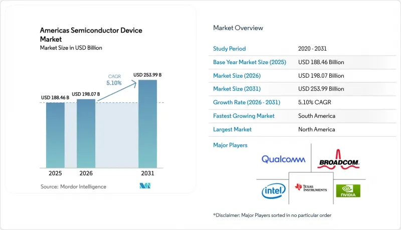
根據 Mordor Intelligence 預測,北美和南美半導體裝置市場規模將從 2025 年的 1884.6 億美元成長到 2026 年的 1980.7 億美元,然後在 2031 年達到 2539.9 億美元,2026 年至 2031 年的複合年成長率為 5.1%。
本報告按元件類型(離散半導體、光電子元件、感測器、積體電路)、晶圓尺寸(200 毫米以下、300 毫米、450 毫米以上)、製程節點(65 奈米以上、45-28 奈米、22-16 奈米、其他終端)、半導體材料(矽、工業、產品、其他產業)。
北美和南美半導體裝置市場趨勢與洞察
CHIPS 方法促進了北美製造業產能的擴張。
根據《晶片與科學法案》,聯邦政府的大規模激勵措施吸引了超過4,500億美元的私人投資,旨在2032年將美國國內晶圓產量提高三倍。英特爾獲得了85億美元的津貼,用於其跨州擴張計劃;台積電獲得了66億美元的津貼,用於在亞利桑那州建造兩座大型晶圓廠。為了縮短前置作業時間,40多家一級化學和設備製造商在附近建立了工廠,圍繞著這些項目形成了供應商生態系統。雖然這種叢集降低了物流成本並加速了技術轉移,但美國對60%的特種氣體和化學品的進口依賴程度仍然沒有改變,仍然需要新的資本投資來擴大國內材料生產能力。最終,這波投資熱潮為北美和南美半導體元件市場實現更高程度的自給自足奠定了基礎,儘管它並沒有使這些市場完全擺脫資源限制。
墨西哥和巴西對配備ADAS系統的車輛的需求
電氣化和L2級駕駛輔助系統的引入,使得墨西哥和巴西主要組裝上的每輛車所用汽車半導體數量在2024年前增加了35%。當地工廠採用了雷達、LiDAR和影像感測器陣列,這些都需要高度可靠的微控制器和功率裝置。博世和大陸集團推動成立了一家合資企業,在當地建造封裝生產線,以應對可能高達25%的進口關稅。政策制定者暗示將對汽車晶片提供額外的稅額扣抵,以鼓勵進一步擴大產能。因此,汽車訂單保護了北美和南美半導體裝置市場免受消費性電子產品市場波動的影響,並帶來了穩健的中期收入成長。
美國西南部製造工廠面臨水電供應限制
亞利桑那州和德克薩斯州新建的晶圓廠每天消耗高達1000萬加侖的超純水,直接與公眾用水形成競爭。英特爾投資2億美元建立了一套循環利用系統,可回收90%的製程用水,但這些環保計畫使營運成本增加了2%,並且無法完全消除長期乾旱的風險。電力需求的成長迫使電力公司加快電網升級,進一步推高了生產成本。這些限制因素降低了《晶片法案》(CHIPS Act)獎勵所推動的實際產能成長,從長遠來看,這將威脅北美和南美半導體裝置市場的成本競爭力。
細分市場分析
預計2025年,積體電路(IC)將佔銷售額的80.65%,複合年成長率(CAGR)為7.45%。北美和南美半導體裝置市場仍嚴重偏向複雜邏輯和記憶體。在人工智慧訓練、自動駕駛和工業邊緣運算等領域中,每個系統矽用量的增加推高了高頻寬記憶體和推理加速器的平均售價。分離式功率裝置雖然市場規模較小,但在電動車領域日益重要,因為碳化矽(SiC)和氮化鎵(GaN)開關正在取代矽IGBT,從而提高了動力傳動系統的效率和熱裕度。北美和南美半導體裝置產業的光電元件業務已擴展到雷射雷達(LiDAR)和影像感測領域,進一步拓展了其在週期性智慧型手機市場的業務。
由於嵌入式應用日益多元化,感測器出貨量保持強勁,但由於許多設計依賴於成熟的製程生產線(這些生產線的資產已完全折舊免稅額),價格壓力依然存在。類比IC透過傳統的汽車和工業插座提供穩定的現金流,這需要數十年的持續供應。另一方面,邏輯和記憶體的波動性更大,反映了超大規模公司的資本支出週期。儘管存在這些波動,對積體電路生態系統的持續投資以及北美和南美半導體裝置市場設計人才的留存仍在繼續。
到2025年,300毫米生產線將佔總產量的57.60%,幾乎支援所有最先進的製程節點,並佔據北美和南美半導體裝置市場的最大佔有率。代工廠已將成熟的類比產品從200毫米電路板轉移基板,從而降低了30%的單位成本並提高了毛利率。同時,設備製造商正在推進450毫米試製設備的改良。雖然這直徑的電路板目前仍屬於小眾市場,但隨著製造商追求更大的規模經濟效益,預計到2031年,其複合年成長率將達到16.4%。
由於汽車和工業領域的買家優先考慮的是可靠性而非單純的運算密度,因此200毫米及以下晶圓廠仍佔據重要地位。這些晶圓廠也受惠於後端組裝在墨西哥的近岸外包,從而縮短了傳統組件的生產週期。北美和南美半導體裝置市場持續平衡各直徑晶圓廠的投資,以因應特定節點和晶圓尺寸的週期性供應過剩。
其他好處:
- Excel格式的市場預測(ME)表
- 3個月的分析師支持
目錄
第1章:引言
- 研究假設和市場定義
- 調查範圍
第2章:調查方法
第3章執行摘要
第4章 市場狀況
- 市場概覽
- 市場促進因素
- CHIPS 方法推動了北美半導體製造能力的擴張。
- 墨西哥和巴西對配備ADAS系統的車輛的需求
- 5G獨立組網系統的部署增加了射頻前端積體電路的消耗量。
- 超大規模人工智慧伺服器的擴張增加了對 HBM 和 GPU 的需求。
- 巴西和智利將透過可再生能源激勵措施來促進功率半導體的採用。
- 將後端組裝檢驗業務外包至墨西哥
- 市場限制因素
- 美國西南部製造工廠面臨水電供應限制
- 北美和南美半導體裝置行業普遍缺乏熟練的半導體工程師
- 對先進設備和智慧財產權的出口限制
- 由於區域供不應求,矽晶圓價格出現波動
- 價值鏈分析
- 監理展望
- 波特五力模型
- 投資與生產能力分析
- 宏觀經濟因素的影響
第5章 市場規模與成長預測
- 依設備類型
- 法令半導體
- 光電子學
- 感應器
- 積體電路
- 類比IC
- 邏輯積體電路
- 記憶
- 微型積體電路
- 微處理器(MPU)
- 微控制器(MCU)
- 數位訊號處理器(DSP)
- 按晶圓尺寸
- 200毫米或更小
- 300 mm
- 450毫米或以上
- 按行程節點
- 65奈米或更小
- 45~28 nm
- 22~16 nm
- 10~7 nm
- 5奈米或更小
- 透過半導體材料
- 矽(Si)
- 碳化矽(SiC)
- 氮化鎵(GaN)
- 其他(GaAs、InP 等)
- 按最終用戶行業分類
- 車
- 通訊(有線和無線)
- 家用電子產品
- 產業
- 計算和數據存儲
- 航太/國防
- 醫療保健和醫療設備
- 按地區
- 北美洲
- 美國
- 加拿大
- 南美洲
- 巴西
- 阿根廷
- 墨西哥
- 其他南美國家
- 北美洲
第6章 競爭情勢
- 市場集中度
- 策略趨勢
- 市佔率分析
- 公司簡介
- Intel Corporation
- NVIDIA Corporation
- Qualcomm Incorporated
- Micron Technology Inc.
- Texas Instruments Incorporated
- Broadcom Inc.
- Advanced Micro Devices Inc.
- onsemi(ON Semiconductor Corporation)
- NXP Semiconductors NV
- Infineon Technologies AG
- STMicroelectronics NV
- Analog Devices Inc.
- Microchip Technology Inc.
- Skyworks Solutions Inc.
- GlobalFoundries Inc.
- Taiwan Semiconductor Manufacturing Company Limited
- Samsung Electronics Co., Ltd.
- Marvell Technology Inc.
- Monolithic Power Systems
- Wolfspeed Inc.
- Lattice Semiconductor
第7章 市場機會與未來展望
According to Mordor Intelligence, the americas semiconductor device market size is expected to grow from USD 188.46 billion in 2025 to USD 198.07 billion in 2026 and is forecast to reach USD 253.99 billion by 2031 at 5.1% CAGR over 2026-2031.
This report is Segmented by Device Type (Discrete Semiconductors, Optoelectronics, Sensors, and Integrated Circuits), Wafer Size (<= 200 Mm, 300 Mm, and >= 450 Mm), Technology Node (>= 65 Nm, 45-28 Nm, 22-16 Nm, and More), Semiconductor Material (Silicon, Silicon Carbide, and More), End-User Vertical (Automotive, Communication, Consumer, Industrial, and More), and by Region (North America, and South America).
Americas Semiconductor Device Market Trends and Insights
CHIPS Act-Driven Fabrication Capacity Expansion in North America
Massive federal incentives under the CHIPS and Science Act unlocked more than USD 450 billion in private commitments that aimed to triple domestic wafer output by 2032. Intel secured USD 8.5 billion in grants for multistate expansions, while TSMC received USD 6.6 billion for its two Arizona megafabs. Supplier ecosystems clustered around those projects, as over 40 tier-one chemical and equipment firms co-located nearby to shorten lead times. These clusters improved logistics costs and accelerated knowledge transfer, yet a 60% dependence on imported specialty gases and chemicals still forced new capital outlays for on-shore materials capacity. Ultimately, the investment surge positioned the Americas semiconductor device market for higher self-sufficiency without fully insulating it from resource constraints.
ADAS-Enabled Vehicle Demand in Mexico and Brazil
Electrification and Level-2 driver-assistance adoption pushed automotive semiconductor content per vehicle up 35% in leading Mexican and Brazilian assembly lines during 2024. Local plants integrated radar, lidar, and image-sensor arrays that required high-reliability microcontrollers and power devices. Bosch and Continental pursued joint ventures for on-shore packaging lines to mitigate import tariffs that could rise to 25%. Policymakers signalled additional fiscal credits for auto-grade chips, encouraging further capacity moves. As a result, automotive orders buffered the Americas semiconductor device market against consumer-electronics cyclicality and created a dependable mid-term revenue uplift.
Water and Power Supply Constraints in U.S. Southwest Fabs
New fabs in Arizona and Texas consumed up to 10 million gallons of ultrapure water daily, creating direct competition with municipal users. Intel invested USD 200 million in reclamation systems that recycled 90% of process water, yet those eco-projects added 2% to operating expenses and did not fully mitigate long-term drought risk. Rising electricity demand forced utilities to accelerate grid upgrades, further lifting production costs. These constraints reduced effective capacity gains from CHIPS Act incentives and threatened the cost competitiveness of the Americas semiconductor device market over the long horizon.
Other drivers and restraints analyzed in the detailed report include:
- 5G Stand-Alone Roll-out Elevating RF Front-End IC Consumption
- Hyperscale AI Server Build-out Increasing HBM and GPU Requirements
- Scarcity of Skilled Semiconductor Engineers across the Americas
For complete list of drivers and restraints, kindly check the Table Of Contents.
Segment Analysis
Integrated circuits captured 80.65% revenue in 2025 and advanced on a 7.45% CAGR projection, keeping the Americas semiconductor device market size firmly weighted toward complex logic and memory. AI training, autonomous driving, and industrial edge computing each increased silicon content per system, lifting average selling prices for high-bandwidth memory and inference accelerators. Discrete power devices, though smaller in value, gained strategic importance as silicon-carbide and gallium-nitride switches replaced silicon IGBTs in electric vehicles, improving powertrain efficiency and thermal margins. The Americas semiconductor device industry also saw optoelectronics broaden into lidar and image-sensing, providing incremental diversification against the cyclic smartphone segment.
A widening array of embedded applications drove resilient sensor volumes, yet price pressure persisted because many designs relied on mature process lines with fully depreciated assets. Analog ICs offered stable cash flow due to legacy automotive and industrial sockets that require decades-long supply continuity. Meanwhile, logic and memory displayed higher volatility in line with hyperscale capex cycles. Despite those swings, the integrated-circuits category delivered steady ecosystem investment, reinforcing design talent retention inside the Americas semiconductor device market.
In 2025, 300 mm lines accounted for 57.60% of production and underpinned nearly every leading-edge node, anchoring the largest slice of the Americas semiconductor device market size. Foundries noted 30% lower unit costs after migrating mature analog products from 200 mm to 300 mm substrates, widening gross-margin cushions. Equipment makers concurrently refined 450 mm pilot tools; although that diameter remained niche, it logged a 16.4% CAGR outlook to 2031 as manufacturers chased further economies of scale.
<=200 mm fabs preserved relevance because automotive and industrial buyers valued proven reliability over raw compute density. These fabs also benefited from the near-shoring of backend assembly in Mexico, which reduced cycle times for legacy components. The Americas semiconductor device market continued to balance investments across diameters to hedge against cyclical oversupply at any single node or wafer size.
Complete Report Scope:
- By Device Type
- Discrete Semiconductors
- Optoelectronics
- Sensors
- Integrated Circuits
- Analog ICs
- Logic ICs
- Memory ICs
- Micro ICs
- Microprocessors (MPU)
- Microcontrollers (MCU)
- Digital Signal Processors (DSP)
- By Wafer Size
- <= 200 mm
- 300 mm
- >= 450 mm
- By Technology Node
- >= 65 nm
- 45-28 nm
- 22-16 nm
- 10-7 nm
- <= 5 nm
- By Semiconductor Material
- Silicon (Si)
- Silicon Carbide (SiC)
- Gallium Nitride (GaN)
- Others (GaAs, InP, etc.)
- By End-User Vertical
- Automotive
- Communication (Wired and Wireless)
- Consumer Electronics
- Industrial
- Computing and Data Storage
- Aerospace and Defense
- Healthcare and Medical Devices
- By Region
- North America
- United States
- Canada
- South America
- Brazil
- Argentina
- Mexico
- Rest of South America
- North America
List of Companies Covered in this Report:
- Intel Corporation
- NVIDIA Corporation
- Qualcomm Incorporated
- Micron Technology Inc.
- Texas Instruments Incorporated
- Broadcom Inc.
- Advanced Micro Devices Inc.
- onsemi (ON Semiconductor Corporation)
- NXP Semiconductors N.V.
- Infineon Technologies AG
- STMicroelectronics N.V.
- Analog Devices Inc.
- Microchip Technology Inc.
- Skyworks Solutions Inc.
- GlobalFoundries Inc.
- Taiwan Semiconductor Manufacturing Company Limited
- Samsung Electronics Co., Ltd.
- Marvell Technology Inc.
- Monolithic Power Systems
- Wolfspeed Inc.
- Lattice Semiconductor
Additional Benefits:
- The market estimate (ME) sheet in Excel format
- 3 months of analyst support
TABLE OF CONTENTS
1 INTRODUCTION
- 1.1 Study Assumptions and Market Definition
- 1.2 Scope of the Study
2 RESEARCH METHODOLOGY
3 EXECUTIVE SUMMARY
4 MARKET LANDSCAPE
- 4.1 Market Overview
- 4.2 Market Drivers
- 4.2.1 CHIPS Act-Driven Fabrication Capacity Expansion in North America
- 4.2.2 ADAS-Enabled Vehicle Demand in Mexico and Brazil
- 4.2.3 5G Stand-Alone Roll-out Elevating RF Front-End IC Consumption
- 4.2.4 Hyperscale AI Server Build-out Increasing HBM and GPU Requirements
- 4.2.5 Renewable-Energy Incentives Boosting Power Semiconductor Adoption in Brazil and Chile
- 4.2.6 Nearshoring of Backend Assembly and Test to Mexico
- 4.3 Market Restraints
- 4.3.1 Water and Power Supply Constraints in US Southwest Fabs
- 4.3.2 Scarcity of Skilled Semiconductor Engineers across Americas
- 4.3.3 Export Controls on Advanced Equipment and IP
- 4.3.4 Volatile Silicon Wafer Pricing due to Limited Regional Supply
- 4.4 Value Chain Analysis
- 4.5 Regulatory Outlook
- 4.6 Porter's Five Forces
- 4.6.1 Bargaining Power of Suppliers
- 4.6.2 Bargaining Power of Buyers
- 4.6.3 Threat of New Entrants
- 4.6.4 Threat of Substitutes
- 4.6.5 Intensity of Competitive Rivalry
- 4.7 Investment and Capacity Analysis
- 4.8 Impact of Macroeconomic Factors
5 MARKET SIZE AND GROWTH FORECASTS (VALUE)
- 5.1 By Device Type
- 5.1.1 Discrete Semiconductors
- 5.1.2 Optoelectronics
- 5.1.3 Sensors
- 5.1.4 Integrated Circuits
- 5.1.4.1 Analog ICs
- 5.1.4.2 Logic ICs
- 5.1.4.3 Memory ICs
- 5.1.4.4 Micro ICs
- 5.1.4.4.1 Microprocessors (MPU)
- 5.1.4.4.2 Microcontrollers (MCU)
- 5.1.4.4.3 Digital Signal Processors (DSP)
- 5.2 By Wafer Size
- 5.2.1 <= 200 mm
- 5.2.2 300 mm
- 5.2.3 >= 450 mm
- 5.3 By Technology Node
- 5.3.1 >= 65 nm
- 5.3.2 45-28 nm
- 5.3.3 22-16 nm
- 5.3.4 10-7 nm
- 5.3.5 <= 5 nm
- 5.4 By Semiconductor Material
- 5.4.1 Silicon (Si)
- 5.4.2 Silicon Carbide (SiC)
- 5.4.3 Gallium Nitride (GaN)
- 5.4.4 Others (GaAs, InP, etc.)
- 5.5 By End-User Vertical
- 5.5.1 Automotive
- 5.5.2 Communication (Wired and Wireless)
- 5.5.3 Consumer Electronics
- 5.5.4 Industrial
- 5.5.5 Computing and Data Storage
- 5.5.6 Aerospace and Defense
- 5.5.7 Healthcare and Medical Devices
- 5.6 By Region
- 5.6.1 North America
- 5.6.1.1 United States
- 5.6.1.2 Canada
- 5.6.2 South America
- 5.6.2.1 Brazil
- 5.6.2.2 Argentina
- 5.6.2.3 Mexico
- 5.6.2.4 Rest of South America
- 5.6.1 North America
6 COMPETITIVE LANDSCAPE
- 6.1 Market Concentration
- 6.2 Strategic Moves
- 6.3 Market Share Analysis
- 6.4 Company Profiles (includes Global level Overview, Market level overview, Core Segments, Financials as available, Strategic Information, Market Rank/Share for key companies, Products and Services, and Recent Developments)
- 6.4.1 Intel Corporation
- 6.4.2 NVIDIA Corporation
- 6.4.3 Qualcomm Incorporated
- 6.4.4 Micron Technology Inc.
- 6.4.5 Texas Instruments Incorporated
- 6.4.6 Broadcom Inc.
- 6.4.7 Advanced Micro Devices Inc.
- 6.4.8 onsemi (ON Semiconductor Corporation)
- 6.4.9 NXP Semiconductors N.V.
- 6.4.10 Infineon Technologies AG
- 6.4.11 STMicroelectronics N.V.
- 6.4.12 Analog Devices Inc.
- 6.4.13 Microchip Technology Inc.
- 6.4.14 Skyworks Solutions Inc.
- 6.4.15 GlobalFoundries Inc.
- 6.4.16 Taiwan Semiconductor Manufacturing Company Limited
- 6.4.17 Samsung Electronics Co., Ltd.
- 6.4.18 Marvell Technology Inc.
- 6.4.19 Monolithic Power Systems
- 6.4.20 Wolfspeed Inc.
- 6.4.21 Lattice Semiconductor
7 MARKET OPPORTUNITIES AND FUTURE OUTLOOK
- 7.1 White-space and Unmet-Need Assessment

 亞太地區半導體元件:市場佔有率分析、產業趨勢與統計及成長預測(2026-2031)日本半導體裝置:市場佔有率分析、產業趨勢與統計、成長預測(2026-2031)歐洲半導體裝置:市場佔有率分析、產業趨勢與統計數據、成長預測(2026-2031)光敏半導體元件:市場佔有率分析、產業趨勢與統計、成長預測(2026-2031)
 2034年工業半導體市場預測-全球分析(依元件類型、材料、封裝類型、功率等級、晶圓尺寸、應用、終端用戶產業、製造模式、銷售管道和地區分類)
 半導體拆解服務市場:全球市場預測,2026-2032年用於加工應用的半導體裝置:市場佔有率分析、行業趨勢和統計數據以及成長預測(2026-2031 年)
 光敏半導體元件市場:依元件、材料、應用、工作模式、最終用戶、國家及地區分類-全球產業分析、市場規模、市場佔有率及2026年至2033年預測半導體裝置:市場佔有率分析、產業趨勢與統計、成長預測(2025-2030)
 半導體環境感測器市場分析與預測(至2035年):類型、產品類型、技術、組件、應用、材料類型、最終用戶、功能、安裝方式、解決方案