


 |
市場調查報告書
商品編碼
2044016
工業半導體矽晶圓:市場佔有率分析、產業趨勢與統計、成長預測(2026-2031)Industrial Semiconductor Silicon Wafer - Market Share Analysis, Industry Trends & Statistics, Growth Forecasts (2026 - 2031) |
||||||
※ 本網頁內容可能與最新版本有所差異。詳細情況請與我們聯繫。
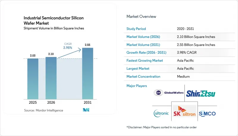
預計工業半導體矽晶圓市場將從 2025 年的 20.3 億平方英寸和 2026 年的 21 億平方英寸成長到 2031 年的 25.5 億平方英寸,2026 年至 2031 年的複合年成長率為 3.98%。
雖然大部分成長歸功於300毫米基板(其已佔總消耗量的近一半),但用於碳化矽(SiC)功率裝置的200毫米外延晶圓和用於光子學的絕緣體上矽(SOI)光電的市場佔有率也在加速擴張。記憶體領域投資的復甦、環柵(GAA)邏輯裝置更嚴格的平整度要求以及到2025年庫存正常化等因素,都推動了出貨量的成長。中國創紀錄的晶圓投資、歐洲加強供應鏈韌性的努力以及美國《晶片製造和整合產品法案》(CHIPS Act)提供的補貼,正在重塑產能決策,這些因素往往比單純的成本考量更為重要。氦氣價格飆升、200毫米設備的過時以及封裝造成的翹曲仍然是主要的營運風險。同時,現有企業正在利用人工智慧驅動的晶體生長控制技術,並重新投入資源以應對成本壓力並維持利潤率。
全球工業半導體矽晶圓市場趨勢與洞察
電動車的廣泛普及以及向800V車輛平台的過渡
電池式電動車(BEV)車型正從400V系統過渡到800V系統。這將縮短充電時間並減輕佈線重量,但需要使用在200mm外延晶圓上製造的SiC MOSFET。 2024年,英飛凌透過人工智慧驅動的晶體生長製程最佳化,將200mm SiC的良率提高了約85%,在不相應增加資本投入的情況下,實現了產量翻倍。同年,Wolfspeed將200mm SiC晶圓的成本降低了30%,進一步拉大了與傳統矽元件的價格差距。中國的比亞迪和蔚來汽車率先採用了800V系統,確保了國內基板供應,但也導致全球前置作業時間延長至26週以上。因此,200mm晶圓的短缺不僅是週期性的庫存問題,而是向電動車轉型所帶來的必然結果。
800V充電基礎設施快速發展
歐洲的「替代燃料基礎設施法規」要求到2025年,主要高速公路沿線每隔60公里安裝一個高功率充電樁,預計2024年至2025年間將建成超過5萬個超快充電站。中國國家電網公司計畫在2025年運作超過10萬個350kW的新型充電樁,每個功率模組均採用多個SiC或GaN晶片。 ABB等充電設備製造商已簽署多年200mm晶圓供應契約,進一步收緊現貨市場,並提振了市場需求。
200mm基板供不應求
由於設備製造商幾乎完全停止了200毫米設備的研發,晶圓廠被迫依賴前置作業時間長的再加工生產線,導致結構性供不應求持續存在。即使Okmetic公司將其在芬蘭的產能提升至5萬片晶圓,也僅佔全球需求的不到2%,無法緩解汽車產業長達26週的等待時間。隨著大型整合裝置製造商(IDM)將其類比工作負載轉向300毫米,小眾廠商面臨著更緊張的產能分配。
細分市場分析
預計到2025年,300毫米晶圓將佔工業半導體矽晶圓市場的48.62%,年複合成長率達4.85%,這主要得益於各大邏輯和記憶體晶圓廠致力於提高單次加工晶片數量。三星和SK海力士正在加速300毫米空白晶圓的消耗,計劃在2026年將其DRAM產量的五分之一以上用於高頻寬記憶體。甚至模擬IDM廠商也考慮遷移到300毫米晶圓,以避開200毫米晶圓的瓶頸。
在射頻、感測器和光電子領域,由於傳統設備足以滿足需求且資本投入適中,對小直徑晶圓的需求仍然存在。然而,混合鍵合和穿透矽通孔(TSV)封裝對平整度的要求極高,只有300mm基板才能滿足這項要求,這實際上將許多先進專案限制在了大直徑晶圓領域。以國家矽產業集團為首的中國供應商正加大對通用型300mm晶圓的投入,每月供應超過100萬片晶圓,對日本的市場主導地位構成挑戰。
《工業半導體矽晶圓市場報告》以晶圓直徑(150毫米及以下、200毫米、300毫米)、半導體裝置類型(邏輯元件、記憶體、模擬器等)、晶圓類型(拋光面、外延面、SOI、特種矽)和地區(北美、歐洲、亞太類型、南美、中東和非洲)進行細分。市場預測以體積(平方英吋)為單位。
區域分析
至2025年,亞太地區將佔全球消費量的82.39%,並維持4.15%的複合年成長率,鞏固其作為工業半導體矽晶圓市場領先地區的地位。光是中國在2025年上半年就投資4,550億元人民幣(約633億美元)擴大前端產能,其中超過一半用於基板。台灣地區專注於尖端邏輯裝置,韓國專注於記憶體,而日本則專注於寬能隙和SOI中試生產線。
北美雖然規模仍相對較小,但正經歷快速成長,這得益於《晶片法案》(CHIPS Act)的資金支持。該法案促使GlobalWafers公司在德克薩斯投資35億美元的工廠,並在同年宣布追加40億美元的擴建計畫。 SK Siltron公司位於密西根州的工廠預算為36億美元,預計2027年將新增300毫米晶圓產能。加拿大和墨西哥則負責後端加工,從而推動了回收晶圓和測試晶圓的需求。
歐洲正透過430億歐元(473億美元)的《晶片法案》(CHIPS Act)穩定其市場佔有率,並支持Siltronic在新加坡投資20億歐元(22億美元)的「Fab-Next」項目,以服務兩個地區的客戶。德國和法國優先考慮模擬和功率半導體的自給自足,並在全球邁進300毫米的同時,仍保持200毫米製程的重要性。其他地區合計市場佔有率不足2%,但正在探索與碳化矽(SiC)相關的舉措,以履行其對可再生能源的承諾。
其他好處:
- Excel格式的市場預測(ME)表
- 3個月的分析師支持
目錄
第1章:引言
- 研究假設和市場定義
- 調查範圍
第2章:調查方法
第3章執行摘要
第4章 市場狀況
- 市場概覽
- 產業價值鏈分析
- 監理情勢
- 技術展望
- 宏觀經濟因素對市場的影響
- 波特五力分析
- 供應商的議價能力
- 買方的議價能力
- 新進入者的威脅
- 替代品的威脅
- 競爭公司之間的競爭
- 市場促進因素
- 電動車的廣泛普及以及向800V車輛平台的過渡
- 800V充電基礎設施快速發展
- 與矽相比,具有更優異的高溫和高頻性能。
- 政府對寬能隙裝置製造的獎勵
- 人工智慧驅動的對 3D IC 矽光子光電的需求,使得超平坦的 SOI 晶圓成為必要。
- 晶圓回收和循環經濟的需求將降低 300 毫米生產線的總擁有成本。
- 市場限制因素
- 200mm基板供不應求
- 資本密集型晶體生長裝置
- 包裝引起的熱機械應力
- 氦氣供應即將受到限制,這將影響化學機械拋光和外延設備。
第5章 市場規模與成長預測
- 依晶圓直徑
- 最大可達 150 毫米
- 200 mm
- 300 mm
- 依半導體裝置類型
- 邏輯
- 記憶
- 模擬
- 離散的
- 其他半導體裝置(光電子裝置、感測器、微型元件)
- 依晶片類型
- 拋光
- 外延
- 絕緣體上矽(SOI)
- 特種矽(高電阻、高功率、感測器級)
- 按地區
- 北美洲
- 美國
- 加拿大
- 墨西哥
- 歐洲
- 德國
- 英國
- 法國
- 其他歐洲地區
- 亞太地區
- 中國
- 日本
- 印度
- 韓國
- 台灣
- 亞太其他地區
- 南美洲
- 中東
- 非洲
- 北美洲
第6章 競爭情勢
- 市場集中度
- 策略趨勢
- 市佔率分析
- 公司簡介
- Shin-Etsu Chemical Co., Ltd.
- SUMCO Corporation
- GlobalWafers Co., Ltd.
- Siltronic AG
- SK Siltron Co., Ltd.
- Soitec SA
- Okmetic Oy
- Wafer Works Corp.
- National Silicon Industry Group(NSIG)
- Zhonghuan Advanced Semiconductor Materials
- QL Electronics
- Nanjing Guosheng Electronics
- Hebei Puxing Electronic Technology
- Shanghai Advanced Silicon Technology(AST)
- Ferrotec Holdings Corporation
- Topsil Semiconductor Materials
- Retain GlobalWafers Co.,
- Simgui
- GRINM Semiconductor Materials
- ESWIN Technology Group
- Formosa Sumco Technology Corp.
第7章 市場機會與未來展望
The industrial semiconductor silicon wafer market size is projected to expand from 2.03 billion square inches in 2025 and 2.10 billion square inches in 2026 to 2.55 billion square inches by 2031, registering a CAGR of 3.98% between 2026 and 2031.
Most of the incremental area will come from 300 mm substrates, which already account for nearly half of total consumption, while 200 mm epitaxial wafers for silicon-carbide (SiC) power devices and silicon-on-insulator (SOI) wafers for photonics accelerate their mix gains. A rebound in memory spending, tighter flatness requirements for gate-all-around logic, and inventory normalization in 2025 have together lifted shipment momentum. China's record wafer investments, Europe's push for supply-chain resilience, and the United States' CHIPS Act subsidies are reshaping capacity decisions, often overriding pure cost considerations. Helium price spikes, 200 mm tool obsolescence, and packaging-induced warpage remain the chief operational risks. Meanwhile, incumbents use AI-based crystal-growth controls and reclaim initiatives to offset cost pressure and preserve margins.
Global Industrial Semiconductor Silicon Wafer Market Trends and Insights
Rising EV Penetration And Shift Toward 800-V Vehicle Platforms
Battery-electric models are migrating from 400-V to 800-V systems, which cuts charging time and wiring weight, but requires SiC MOSFETs processed on 200 mm epitaxial wafers. Infineon boosted 200 mm SiC yields by nearly 85% in 2024 through AI-optimized crystal growth, letting the firm double output without proportional capex. Wolfspeed achieved a 30% cost reduction in 200 mm SiC wafers that same year, widening the price gap with legacy silicon devices. Chinese brands BYD and NIO adopted 800 V early, locking in domestic substrate supply and extending global lead times beyond 26 weeks. Tight 200 mm availability is therefore an outgrowth of the EV transition and not merely a cyclical inventory issue.
Rapid Build-Out Of 800 V Charging Infrastructure
The European Alternative Fuels Infrastructure Regulation mandates high-power chargers every 60 km along core corridors by 2025, triggering more than 50,000 ultra-fast installations in 2024-2025.China's State Grid commissioned over 100,000 new 350 kW ports in 2025, each power module containing multiple SiC or GaN die. Charging-equipment makers such as ABB sign multiyear 200 mm wafer contracts to protect supply, further straining the spot market and reinforcing demand visibility.
Limited Availability Of 200 MM Substrates
Toolmakers have largely frozen new 200 mm equipment development, so fabs depend on refurbished lines with longer lead times, locking in a structural shortage. Okmetic's 50,000-wafer capacity addition in Finland adds less than 2% to global demand and fails to ease 26-week automotive waits. As large IDMs migrate analog workloads to 300 mm, niche players face even tighter allocations.
Other drivers and restraints analyzed in the detailed report include:
- High-Temperature, High-Frequency Advantages Over Silicon
- Government Incentives For Wide-Band-Gap Fabs
- Capital-Intensive Crystal-Growth Equipment
For complete list of drivers and restraints, kindly check the Table Of Contents.
Segment Analysis
The 300 mm portion of the industrial semiconductor silicon wafer market size commanded 48.62% in 2025 and is on track for a 4.85% CAGR as leading logic and memory fabs seek larger die counts per pass. Samsung and SK Hynix dedicated more than one-fifth of their DRAM starts to high-bandwidth memory in 2026, accelerating consumption of 300 mm blanks. Even analog IDMs now explore 300 mm conversions to escape 200 mm bottlenecks.
Smaller diameters retain relevance in RF, sensors, and optoelectronics where legacy tools suffice and capex is modest. However, hybrid bonding and through-silicon-via packaging demand the flatness tolerance achievable only on 300 mm substrates, effectively locking many advanced programs into the larger format. Chinese suppliers, led by National Silicon Industry Group, funnel fresh funding into commodity 300 mm grades, adding over 1 million wafers a month and challenging Japanese dominance.
The Industrial Semiconductor Silicon Wafer Market Report is Segmented by Wafer Diameter (Up To 150 Mm, 200 Mm, and 300 Mm), Semiconductor Device Type (Logic, Memory, Analog, and More), Wafer Type (Prime Polished, Epitaxial, SOI, and Specialty Silicon), and Geography (North America, Europe, Asia-Pacific, South America, Middle East, Africa). The Market Forecasts are Provided in Terms of Volume (Square Inches).
Geography Analysis
Asia-Pacific represented 82.39% of worldwide consumption in 2025, and its 4.15% CAGR keeps the region firmly atop the industrial semiconductor silicon wafer market. China alone spent CNY 455 billion (USD 63.3 billion) on front-end capacity in 1H 2025, funneling more than half into substrates. Taiwan focuses on leading-edge logic, South Korea on memory, and Japan on wide-band-gap and SOI pilot lines.
North America remains smaller but grows quickly as CHIPS Act money underwrites GlobalWafers' USD 3.5 billion Texas fab, with an additional USD 4 billion expansion announced the same year. SK Siltron's Michigan site, budgeted at USD 3.6 billion, will bring fresh 300 mm capacity by 2027. Canada and Mexico handle backend steps, which in turn drive demand for reclaimed or test wafers.
Europe stabilizes its share through the EUR 43 billion (USD 47.3 billion) Chips Act, supporting Siltronic's EUR 2 billion (USD 2.2 billion) Fab-Next in Singapore for dual-region customers. Germany and France emphasize analog and power sovereignty, prolonging 200 mm relevance despite global 300 mm migration. Other regions together hold under 2% share but explore SiC initiatives tied to renewable power ambitions.
- Shin-Etsu Chemical Co., Ltd.
- SUMCO Corporation
- GlobalWafers Co., Ltd.
- Siltronic AG
- SK Siltron Co., Ltd.
- Soitec SA
- Okmetic Oy
- Wafer Works Corp.
- National Silicon Industry Group (NSIG)
- Zhonghuan Advanced Semiconductor Materials
- QL Electronics
- Nanjing Guosheng Electronics
- Hebei Puxing Electronic Technology
- Shanghai Advanced Silicon Technology (AST)
- Ferrotec Holdings Corporation
- Topsil Semiconductor Materials
- Retain GlobalWafers Co.,
- Simgui
- GRINM Semiconductor Materials
- ESWIN Technology Group
- Formosa Sumco Technology Corp.
Additional Benefits:
- The market estimate (ME) sheet in Excel format
- 3 months of analyst support
TABLE OF CONTENTS
1 INTRODUCTION
- 1.1 Study Assumptions and Market Definition
- 1.2 Scope of the Study
2 RESEARCH METHODOLOGY
3 EXECUTIVE SUMMARY
4 MARKET LANDSCAPE
- 4.1 Market Overview
- 4.2 Industry Value-Chain Analysis
- 4.3 Regulatory Landscape
- 4.4 Technological Outlook
- 4.5 Impact of Macroeconomic Factors on the Market
- 4.6 Porter's Five Forces Analysis
- 4.6.1 Bargaining Power of Suppliers
- 4.6.2 Bargaining Power of Buyers
- 4.6.3 Threat of New Entrants
- 4.6.4 Threat of Substitutes
- 4.6.5 Intensity of Competitive Rivalry
- 4.7 Market Drivers
- 4.7.1 Rising EV Penetration and Shift Toward 800-V Vehicle Platforms
- 4.7.2 Rapid Build-Out of 800 V Charging Infrastructure
- 4.7.3 High-Temperature, High-Frequency Performance Advantages over Si
- 4.7.4 Government Incentives for Wide-Band-Gap Fabs
- 4.7.5 AI-Driven Demand for 3D-IC Silicon Photonics Requiring Ultra-Flat SOI Wafers
- 4.7.6 Wafer Reclaim And Circular-Economy Mandates Lowering Total Cost-of-Ownership for 300 mm Lines
- 4.8 Market Restraints
- 4.8.1 Limited Availability of 200 mm Substrates
- 4.8.2 Capital-Intensive Crystal-Growth Equipment
- 4.8.3 Packaging-Induced Thermo-Mechanical Stress
- 4.8.4 Looming Helium Supply Constraints Impacting CMP and Epitaxial Tools
5 MARKET SIZE And GROWTH FORECASTS (VOLUME)
- 5.1 By Wafer Diameter
- 5.1.1 Up to 150 mm
- 5.1.2 200 mm
- 5.1.3 300 mm
- 5.2 By Semiconductor Device Type
- 5.2.1 Logic
- 5.2.2 Memory
- 5.2.3 Analog
- 5.2.4 Discrete
- 5.2.5 Other Semiconductor Device Types (Optoelectronics, Sensors, Micro)
- 5.3 By Wafer Type
- 5.3.1 Prime Polished
- 5.3.2 Epitaxial
- 5.3.3 Silicon-on-Insulator (SOI)
- 5.3.4 Specialty Silicon (High-Resistivity, Power, Sensor-Grade)
- 5.4 By Geography
- 5.4.1 North America
- 5.4.1.1 United States
- 5.4.1.2 Canada
- 5.4.1.3 Mexico
- 5.4.2 Europe
- 5.4.2.1 Germany
- 5.4.2.2 United Kingdom
- 5.4.2.3 France
- 5.4.2.4 Rest of Europe
- 5.4.3 Asia-Pacific
- 5.4.3.1 China
- 5.4.3.2 Japan
- 5.4.3.3 India
- 5.4.3.4 South Korea
- 5.4.3.5 Taiwan
- 5.4.3.6 Rest of Asia-Pacific
- 5.4.4 South America
- 5.4.5 Middle East
- 5.4.6 Africa
- 5.4.1 North America
6 COMPETITIVE LANDSCAPE
- 6.1 Market Concentration
- 6.2 Strategic Moves
- 6.3 Market Share Analysis
- 6.4 Company Profiles (includes Global Level Overview, Market Level Overview, Core Segments, Financials as available, Strategic Information, Market Rank/Share, Products And Services, Recent Developments)
- 6.4.1 Shin-Etsu Chemical Co., Ltd.
- 6.4.2 SUMCO Corporation
- 6.4.3 GlobalWafers Co., Ltd.
- 6.4.4 Siltronic AG
- 6.4.5 SK Siltron Co., Ltd.
- 6.4.6 Soitec SA
- 6.4.7 Okmetic Oy
- 6.4.8 Wafer Works Corp.
- 6.4.9 National Silicon Industry Group (NSIG)
- 6.4.10 Zhonghuan Advanced Semiconductor Materials
- 6.4.11 QL Electronics
- 6.4.12 Nanjing Guosheng Electronics
- 6.4.13 Hebei Puxing Electronic Technology
- 6.4.14 Shanghai Advanced Silicon Technology (AST)
- 6.4.15 Ferrotec Holdings Corporation
- 6.4.16 Topsil Semiconductor Materials
- 6.4.17 Retain GlobalWafers Co.,
- 6.4.18 Simgui
- 6.4.19 GRINM Semiconductor Materials
- 6.4.20 ESWIN Technology Group
- 6.4.21 Formosa Sumco Technology Corp.
7 MARKET OPPORTUNITIES AND FUTURE OUTLOOK
- 7.1 White-Space and Unmet-Need Assessment
 矽晶圓市場-全球產業規模、佔有率、趨勢、機會和預測:按晶圓尺寸、類型、應用、最終用戶、地區和競爭格局分類,2021-2031年
 矽晶圓市場規模、佔有率、趨勢和預測:按晶圓尺寸、類型、應用、最終用途和地區分類,2026-2034 年
 半導體矽晶圓回收市場:依回收製程、晶圓類型、晶圓尺寸、應用領域、產業及最終用戶分類-2026-2032年全球市場預測
 2026-2034年全球太陽能矽晶圓市場規模、佔有率、趨勢和成長分析報告
 5G半導體矽晶圓:市場佔有率分析、產業趨勢與統計及成長預測(2026-2031年)用於功率元件的矽晶圓:市場佔有率分析、行業趨勢和統計數據以及成長預測(2026-2031 年)高阻矽晶圓:市佔率分析、產業趨勢與統計、成長預測(2026-2031 年)
 2026 年至 2035 年太陽能電池用矽晶圓市場的機會、成長要素、產業趨勢分析與預測。中國半導體矽晶圓市場:市場佔有率分析、產業趨勢與統計及成長預測(2026-2031年)亞太地區半導體矽晶圓:市場佔有率分析、產業趨勢與統計及成長預測(2026-2031)