


 |
市場調查報告書
商品編碼
2044004
中國半導體矽晶圓市場:市場佔有率分析、產業趨勢與統計及成長預測(2026-2031年)China Semiconductor Silicon Wafer - Market Share Analysis, Industry Trends & Statistics, Growth Forecasts (2026 - 2031) |
||||||
※ 本網頁內容可能與最新版本有所差異。詳細情況請與我們聯繫。
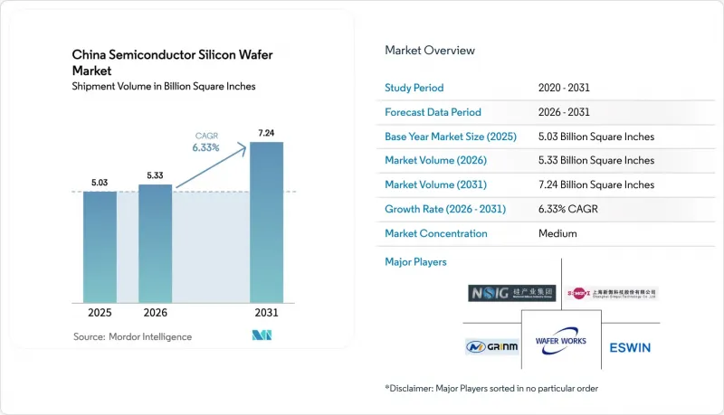
根據以出貨量為準,中國半導體矽晶圓市場預計將從 2025 年的 50.3 億平方英寸成長到 2026 年的 53.3 億平方英寸,到 2031 年將達到 72.4 億平方英寸,2026 年至 2031 年的複合年成長率為 6.33%。
政府強而有力的財政支持、對先進外國設備的更嚴格出口管制以及本土晶圓代工廠加速產能擴張,並持續推動市場需求。北京方面要求自2026年初起實現50%的設備國產化,並將補貼與使用國產製程設備掛鉤,以引導更多晶圓訂單流向中國供應商。邏輯元件和先進模擬元件12吋生產線的快速普及,以及電動車的日益普及,進一步推高了基板總消耗量。基於晶片組的AI加速器需求激增,需要超平整的優質晶圓來實現混合鍵合,這也促進了市場發展。儘管與現有日本製造商相比,缺陷密度差距依然存在,導致高階邏輯元件生產在一定程度上依賴進口。
中國半導體晶圓市場趨勢與洞察
國內廠商迅速擴大300mm產能
中芯國際(SMIC)已確認計劃在2025年底至2026年底前,為其上海、北京和深圳工廠每月新增4萬片12吋晶圓產能。同樣,華宏半導體(HHSC)也正在推進生產計畫。省級政府在土地、稅收和低利率貸款方面的優惠政策降低了初期風險,使得供應商能夠在產能投入運作前簽訂多年期「照付不議」合約。為此,上海矽業集團已將其臨港工廠的12吋晶圓月產能擴大至200萬片,並計畫於2026年交付。優質晶圓單價低於50美元的規模經濟效應已成為一個轉捩點,加速了小規模新創公司之間的整合浪潮,這些企業由於無法在成本上與大型公司競爭而被迫退出市場。
政府強制要求50%的設備生產必須由國內廠商完成,這正在加速國內晶圓需求的成長。
自2026年1月起,工業和資訊化部規定,國產設備採用率達到50%以上是享受補貼的條件,目標是到2028年將此比例提高到70%,並在2030年實現全部國產化。未達到標準的代工廠將被要求退還補貼,因此大多數公司都在精簡供應商名單,並將所有設備和晶圓組合標準化為國產產品。據Nowra Technologies稱,其28nm生產線中超過60%的沉積設備都搭配了上海矽業的晶圓,這使得良率提升週期縮短了近四分之一。這種製程配方的閉合迴路共用加速了缺陷控制的進程,並降低了新晶圓廠的學習曲線。
日本廠商與其他廠商在 28nm 及以上邏輯晶圓的缺陷密度方面持續存在差距。
國產300mm優質晶圓的平均缺陷密度為0.12個缺陷/平方厘米,仍比信越化學的基準值0.08個缺陷/平方厘米高出50%,導致先進移動處理器的良率下降約8-10%。主要原因是在地採購多晶矽中微量金屬污染超過0.1 ppb。代工廠透過延長退火時間和加強進廠檢驗來彌補這一缺陷,導致每片晶圓成本增加15-20美元。因此,從事大規模生產的無廠半導體公司在其尖端產品批次中指定使用日本產基板,儘管產能有所提高,但國產供應商的市場規模仍然有限。
細分市場分析
預計到2025年,300mm晶圓出貨量將佔總出貨量的71.75%,成為中國半導體矽晶圓市場最大的佔有率,並將在2031年之前維持7.16%的複合年成長率。僅中芯國際(SMIC)一家每月新增4萬片12吋晶圓,就足以證明大直徑晶圓在經濟效益上不可逆轉的趨勢。在主流邏輯佈局中,300mm晶圓的晶片良率約為200mm晶圓的2.5倍。這種單晶片成本的降低直接轉化為晶片價格的競爭力,這對於智慧型手機和個人電腦更換週期不斷延長的市場生存至關重要。
200mm晶圓仍然是模擬裝置和碳化矽(SiC)裝置的關鍵應用領域。全球200mm製程設備的短缺已將前置作業時間延長至24週,迫使汽車製造商簽訂多年晶圓供應合約。小於150mm的晶圓主要用於傳統動力傳動系統和工業控制器,但隨著更大直徑晶圓的重新認證勢在必行,它們的作用逐漸被淘汰。儘管如此,中國半導體矽晶圓市場仍在為支援SiC功率模組的6吋和8吋生產線分配專項預算,使該細分市場免受主流300mm晶圓價格下跌的影響。
到2025年,邏輯晶圓將佔總產量的33.37%,反映出其在人工智慧加速器、邊緣處理器和主流SoC領域的主導地位。預計到2031年,該細分市場將以6.82%的複合年成長率成長,超過記憶體和類比晶片領域。這主要得益於國內人工智慧雲端建設的擴張,每個機架都需要消耗數千個高效能處理器。因此,儘管一些尖端晶片仍繼續從日本進口晶圓以確保良率,但中國半導體矽晶圓市場中分配給邏輯應用的規模正在不斷擴大。
儲存晶圓市場成長放緩,主要原因是國內DRAM和NAND快閃產能持續小規模。另一方面,分離式功率元件(主要是SiC MOSFET)在低基數的基礎上實現了中等個位數的高速成長。類比裝置市場的成長主要由電池管理IC和汽車感測技術驅動,但邏輯裝置市場仍是中國政府推動「運算主權」策略的重點。此外,需求多元化意味著邏輯晶圓的需求受單一終端市場經濟波動的影響較小,從而鞏固了其在整體消費中的核心地位。
《中國半導體晶圓市場報告》依晶圓直徑(150mm以下、200mm、300mm)、半導體裝置類型(邏輯元件、記憶體、其他)、晶圓類型(拋光面、外延面、絕緣體上矽(SOI)、特種矽電子)、終端使用者(消費外延面、絕緣體上矽(SOI)、特種矽電子)、終端使用者(消費性電子、工業進行區隔。市場預測以出貨量(平方英吋)為單位。
其他好處
- Excel格式的市場預測(ME)表
- 3個月的分析師支持
目錄
第1章:引言
- 研究假設和市場定義
- 調查範圍
第2章:調查方法
第3章執行摘要
第4章 市場狀況
- 市場概覽
- 市場促進因素
- 國內企業300mm製程生產能力快速成長
- 政府「50%工具國產化」的強制規定正在加速本地晶圓需求。
- 汽車領域SiC功率元件的蓬勃發展推動了對200毫米和8吋SiC晶圓的需求。
- 全球200毫米晶圓製造設備短缺,導致中國晶圓廠只能依賴本地晶圓供應。
- 補貼支撐多晶矽價格,增強成本優勢。
- 先進封裝(晶片/X-DFOI)的興起推動了對超平坦優質晶圓的需求不斷成長。
- 市場限制因素
- 在28nm及以上製程的邏輯晶圓方面,日本製造商與其他製造商之間仍存在明顯的缺陷密度差距。
- 美國主導的出口限制限制了獲取重要的 CZ 晶體和 CMP 工具。
- 成熟節點產能過剩和代工廠之間的價格競爭正在給利潤率帶來壓力。
- 超純水和化學廢棄物處理作業人員短缺。
- 產業價值鏈分析
- 技術分析
- 監理情勢
- 宏觀經濟因素的影響
- 波特五力分析
- 供應商的議價能力
- 買方的議價能力
- 新進入者的威脅
- 替代品的威脅
- 競爭公司之間的競爭
第5章 市場規模與成長預測
- 依晶圓直徑
- 150毫米或更小
- 200mm
- 300mm
- 依半導體裝置類型
- 邏輯
- 記憶
- 模擬
- 離散的
- 其他半導體裝置類型(光電子裝置、感測器、微型元件)
- 依晶片類型
- 拋光
- 外延
- 絕緣體上矽(SOI)
- 特種矽(高電阻、高功率、感測器級)
- 最終用戶
- 家用電器
- 手機和智慧型手機
- PC和伺服器
- 工業的
- 溝通
- 車
- 其他終端用戶應用程式
- 家用電器
第6章 競爭情勢
- 市場集中度
- 策略趨勢
- 市佔率分析
- 公司簡介
- National Silicon Industry Group Co. Ltd.
- Shanghai Silicon Industry Group Co. Ltd.(Simgui)
- TCL Zhonghuan Advanced Semiconductor Materials Co. Ltd.
- Hangzhou Lion Microelectronics Co. Ltd.
- Wafer Works(Shanghai)Co. Ltd.
- GRINM Semiconductor Materials Co. Ltd.
- Zhejiang Jinruihong Technologies Co. Ltd.
- Beijing E-SWIN Material Technology Co. Ltd.
- Advanced Semiconductor Manufacturing Corp.(ASM)
- Siltronic AG
- Shin-Etsu Chemical Co. Ltd.
- SUMCO Corp.
- GlobalWafers Co. Ltd.
- SK Siltron Co. Ltd.
- Soitec SA
- Ferrotec(Anhui)Technology Co. Ltd.
- Hangzhou Semiconductor Wafer Co. Ltd.
- Hebei Puxing Semiconductor
- Chongqing Advanced Silicon Technology
- Nanjing Guosheng Electronics
第7章 市場機會與未來展望
The China Semiconductor Silicon Wafer Market size in terms of shipment volume is expected to grow from 5.03 Billion Square Inches in 2025 to 5.33 Billion Square Inches in 2026 and is forecast to reach 7.24 Billion Square Inches by 2031 at 6.33% CAGR over 2026-2031.
Robust government funding, tighter export controls on advanced foreign tools, and accelerating capacity additions by local foundries continue to propel demand. Beijing's 50%-domestic-equipment mandate, in force since early 2026, ties subsidies to the use of home-grown process tools, channeling incremental wafer orders toward Chinese suppliers. Rapid adoption of twelve-inch lines for logic and advanced analog devices, combined with rising electric-vehicle penetration, further elevates total substrate consumption. The market also benefits from surging chiplet-based AI accelerators that require ultra-flat prime wafers to enable hybrid bonding, even as lingering defect-density gaps versus Japanese incumbents keep high-end logic output partially import-dependent.
China Semiconductor Silicon Wafer Market Trends and Insights
Surge in 300 mm Capacity Build-Outs by Domestic Players
Semiconductor Manufacturing International Corporation confirmed late-2025 plans to add 40,000 twelve-inch wafer starts each month across Shanghai, Beijing, and Shenzhen fabs by end-2026, a move mirrored by Hua Hong Semiconductor's additional 20,000-wspm program targeting power-management ICs. Provincial incentives in land, taxes, and low-interest loans reduce upfront risk, allowing suppliers to sign multiyear take-or-pay contracts before capacity comes online. Shanghai Silicon Industry Group responded by scaling its Lingang plant to 2 million twelve-inch wafers a month for 2026 delivery. Scale economics below USD 50 per prime wafer become the tipping point, spurring a consolidation wave among smaller startups that cannot reach cost parity with these leaders.
Government "50% Domestic Tool" Mandate Accelerating Local Wafer Demand
Effective January 2026, the Ministry of Industry and Information Technology links subsidies to a minimum 50% local-tool adoption, ratcheting the threshold to 70% by 2028 and full localization in 2030. Foundries that fall short face subsidy claw-backs, so most streamline vendor lists to all-Chinese tool-and-wafer pairings. Naura Technology documented that over 60% of its deposition tools installed on 28 nm lines were matched with Shanghai Silicon substrates, trimming yield-ramp cycles by almost a quarter. Joint process-recipe sharing inside these closed loops accelerates progress on defect control and flattens the learning curve for new fabs.
Persistent Defect-Density Gap Vs. Japanese Suppliers in above 28 nm Logic Wafers
Average defect density of 0.12 defects cm-2 on domestic 300 mm prime wafers remains 50% above Shin-Etsu's 0.08 defects cm-2 benchmark, translating into roughly 8-10% lower yield for advanced mobile processors. Trace-metal contamination above 0.1 ppb in locally sourced polysilicon is a major contributor. Foundries compensate by implementing longer anneals and tighter incoming inspections, adding USD 15-20 per wafer in costs. High-volume fabless customers, therefore, stipulate Japanese substrates for leading-edge lots, capping the market ceiling for domestic suppliers despite capacity growth.
Other drivers and restraints analyzed in the detailed report include:
- Automotive SiC Power Device Boom Driving 200 mm and 8-Inch SiC Wafer Needs
- Rise of Advanced Packaging (Chiplet / X-DFOI) Lifting Demand for Ultra-Flat Prime Wafers
- U.S.-Led Export Controls Limiting Access to Critical CZ Crystal and CMP Tools
For complete list of drivers and restraints, kindly check the Table Of Contents.
Segment Analysis
The 300 mm category accounted for 71.75% of total volume in 2025, capturing the largest slice of the China semiconductor silicon wafer market share and sustaining a 7.16% CAGR through 2031. Capacity additions of 40,000 twelve-inch wafers per month at Semiconductor Manufacturing International Corporation alone underscore an irreversible pivot toward larger-diameter economics, where each 300 mm substrate yields roughly 2.5 times as many die as a 200 mm equivalent for mainstream logic layouts. Cost-per-die savings flow directly into competitive chip pricing, a survival imperative as smartphone and PC refresh cycles extend.
The 200 mm segment remains essential for analog and silicon-carbide devices; global shortages of 200 mm process tools have elevated lead times to 24 weeks, locking automotive customers into multiyear wafer agreements. Sub-150-mm wafers address legacy powertrain and industrial controllers, but face sunset as requalification to larger diameters becomes unavoidable. Nevertheless, the China semiconductor silicon wafer market continues to allocate niche budget to six-inch and eight-inch lines supporting SiC power modules, insulating this pocket from the price erosion afflicting bulk 300 mm primes.
Logic wafers held 33.37% of 2025 volume, reflecting dominance in AI accelerators, edge processors, and mainstream SoCs. The segment's 6.82% CAGR to 2031 outpaces memory and analog, helped by domestic AI cloud build-outs that each consume thousands of high-end processors per rack. The China semiconductor silicon wafer market size allocated to logic applications therefore widens, even though some leading-edge die continue to import Japanese substrates for yield security.
Memory wafers trail because domestic DRAM and NAND capacity is still small, whereas discrete power devices, chiefly SiC MOSFETs, post high-single-digit growth off a low base. Analog growth comes from battery-management ICs and automotive sensing, but logic remains the strategic focus as Beijing presses compute sovereignty. Diversified demand also shields logic wafer offtake from cyclical swings in a single end-market, reinforcing its anchor status within overall consumption.
The China Semiconductor Silicon Wafer Market Report is Segmented by Wafer Diameter (Up To 150 Mm, 200 Mm, 300 Mm), Semiconductor Device Type (Logic, Memory, and More), Wafer Type (Prime Polished, Epitaxial, Silicon-On-Insulator (SOI), Specialty Silicon), End-User (Consumer Electronics, Industrial, Automotive, and More), and Geography. The Market Forecasts are Provided in Terms of Shipment Volume (Square Inches).
List of Companies Covered in this Report:
- National Silicon Industry Group Co. Ltd.
- Shanghai Silicon Industry Group Co. Ltd. (Simgui)
- TCL Zhonghuan Advanced Semiconductor Materials Co. Ltd.
- Hangzhou Lion Microelectronics Co. Ltd.
- Wafer Works (Shanghai) Co. Ltd.
- GRINM Semiconductor Materials Co. Ltd.
- Zhejiang Jinruihong Technologies Co. Ltd.
- Beijing E-SWIN Material Technology Co. Ltd.
- Advanced Semiconductor Manufacturing Corp. (ASM)
- Siltronic AG
- Shin-Etsu Chemical Co. Ltd.
- SUMCO Corp.
- GlobalWafers Co. Ltd.
- SK Siltron Co. Ltd.
- Soitec S.A.
- Ferrotec (Anhui) Technology Co. Ltd.
- Hangzhou Semiconductor Wafer Co. Ltd.
- Hebei Puxing Semiconductor
- Chongqing Advanced Silicon Technology
- Nanjing Guosheng Electronics
Additional Benefits:
- The market estimate (ME) sheet in Excel format
- 3 months of analyst support
TABLE OF CONTENTS
1 INTRODUCTION
- 1.1 Study Assumptions and Market Definition
- 1.2 Scope of the Study
2 RESEARCH METHODOLOGY
3 EXECUTIVE SUMMARY
4 MARKET LANDSCAPE
- 4.1 Market Overview
- 4.2 Market Drivers
- 4.2.1 Surge in 300 mm Capacity Build-outs by Domestic Players
- 4.2.2 Government "50 % Domestic Tool" Mandate Accelerating Local Wafer Demand
- 4.2.3 Automotive SiC Power Device Boom Driving 200 mm and 8-inch SiC Wafer Needs
- 4.2.4 Tight Global 200 mm Tool Supply Forcing Chinese Fabs to Lock-in Local Wafer Supply
- 4.2.5 Subsidized Polysilicon Price Support Enhancing Cost Advantage
- 4.2.6 Rise of Advanced Packaging (Chiplet / X-DFOI) Lifting Demand for Ultra-Flat Prime Wafers
- 4.3 Market Restraints
- 4.3.1 Persistent Defect-Density Gap vs. Japanese Suppliers in above 28 nm Logic Wafers
- 4.3.2 U.S.-Led Export Controls Limiting Access to Critical CZ Crystal and CMP Tools
- 4.3.3 Margin Pressure from Mature-Node Over-Capacity and Price-War Among Foundries
- 4.3.4 Skills Shortage in Ultra-Pure Water and Chemical Waste Treatment Operations
- 4.4 Industry Value-Chain Analysis
- 4.5 Technology Analysis
- 4.6 Regulatory Landscape
- 4.7 Impact of Macroeconomic Factors
- 4.8 Porter's Five Forces Analysis
- 4.8.1 Bargaining Power of Suppliers
- 4.8.2 Bargaining Power of Buyers
- 4.8.3 Threat of New Entrants
- 4.8.4 Threat of Substitutes
- 4.8.5 Intensity of Competitive Rivalry
5 MARKET SIZE AND GROWTH FORECASTS (VOLUME)
- 5.1 By Wafer Diameter
- 5.1.1 Up to 150 mm
- 5.1.2 200 mm
- 5.1.3 300 mm
- 5.2 By Semiconductor Device Type
- 5.2.1 Logic
- 5.2.2 Memory
- 5.2.3 Analog
- 5.2.4 Discrete
- 5.2.5 Other Semiconductor Device Types (Optoelectronics, Sensors, Micro)
- 5.3 By Wafer Type
- 5.3.1 Prime Polished
- 5.3.2 Epitaxial
- 5.3.3 Silicon-on-Insulator (SOI)
- 5.3.4 Specialty Silicon (High-Resistivity, Power, Sensor-Grade)
- 5.4 By End-user
- 5.4.1 Consumer Electronics
- 5.4.1.1 Mobile and Smartphones
- 5.4.1.2 PCs and Servers
- 5.4.2 Industrial
- 5.4.3 Telecommunications
- 5.4.4 Automotive
- 5.4.5 Other End-user Applications
- 5.4.1 Consumer Electronics
6 COMPETITIVE LANDSCAPE
- 6.1 Market Concentration
- 6.2 Strategic Moves
- 6.3 Market Share Analysis
- 6.4 Company Profiles (includes Global Level Overview, Market Level Overview, Core Segments, Financials as available, Strategic Information, Market Rank/Share, Products and Services, Recent Developments)
- 6.4.1 National Silicon Industry Group Co. Ltd.
- 6.4.2 Shanghai Silicon Industry Group Co. Ltd. (Simgui)
- 6.4.3 TCL Zhonghuan Advanced Semiconductor Materials Co. Ltd.
- 6.4.4 Hangzhou Lion Microelectronics Co. Ltd.
- 6.4.5 Wafer Works (Shanghai) Co. Ltd.
- 6.4.6 GRINM Semiconductor Materials Co. Ltd.
- 6.4.7 Zhejiang Jinruihong Technologies Co. Ltd.
- 6.4.8 Beijing E-SWIN Material Technology Co. Ltd.
- 6.4.9 Advanced Semiconductor Manufacturing Corp. (ASM)
- 6.4.10 Siltronic AG
- 6.4.11 Shin-Etsu Chemical Co. Ltd.
- 6.4.12 SUMCO Corp.
- 6.4.13 GlobalWafers Co. Ltd.
- 6.4.14 SK Siltron Co. Ltd.
- 6.4.15 Soitec S.A.
- 6.4.16 Ferrotec (Anhui) Technology Co. Ltd.
- 6.4.17 Hangzhou Semiconductor Wafer Co. Ltd.
- 6.4.18 Hebei Puxing Semiconductor
- 6.4.19 Chongqing Advanced Silicon Technology
- 6.4.20 Nanjing Guosheng Electronics
7 MARKET OPPORTUNITIES AND FUTURE OUTLOOK
- 7.1 White-Space and Unmet-Need Assessment
 矽晶圓市場-全球產業規模、佔有率、趨勢、機會和預測:按晶圓尺寸、類型、應用、最終用戶、地區和競爭格局分類,2021-2031年
 矽晶圓市場規模、佔有率、趨勢和預測:按晶圓尺寸、類型、應用、最終用途和地區分類,2026-2034 年
 半導體矽晶圓回收市場:依回收製程、晶圓類型、晶圓尺寸、應用領域、產業及最終用戶分類-2026-2032年全球市場預測
 2026-2034年全球太陽能矽晶圓市場規模、佔有率、趨勢和成長分析報告
 5G半導體矽晶圓:市場佔有率分析、產業趨勢與統計及成長預測(2026-2031年)工業半導體矽晶圓:市場佔有率分析、產業趨勢與統計、成長預測(2026-2031)用於功率元件的矽晶圓:市場佔有率分析、行業趨勢和統計數據以及成長預測(2026-2031 年)高阻矽晶圓:市佔率分析、產業趨勢與統計、成長預測(2026-2031 年)
 2026 年至 2035 年太陽能電池用矽晶圓市場的機會、成長要素、產業趨勢分析與預測。亞太地區半導體矽晶圓:市場佔有率分析、產業趨勢與統計及成長預測(2026-2031)