


 |
市場調查報告書
商品編碼
2044012
用於功率元件的矽晶圓:市場佔有率分析、行業趨勢和統計數據以及成長預測(2026-2031 年)Silicon Wafer For Power Devices - Market Share Analysis, Industry Trends & Statistics, Growth Forecasts (2026 - 2031) |
||||||
※ 本網頁內容可能與最新版本有所差異。詳細情況請與我們聯繫。
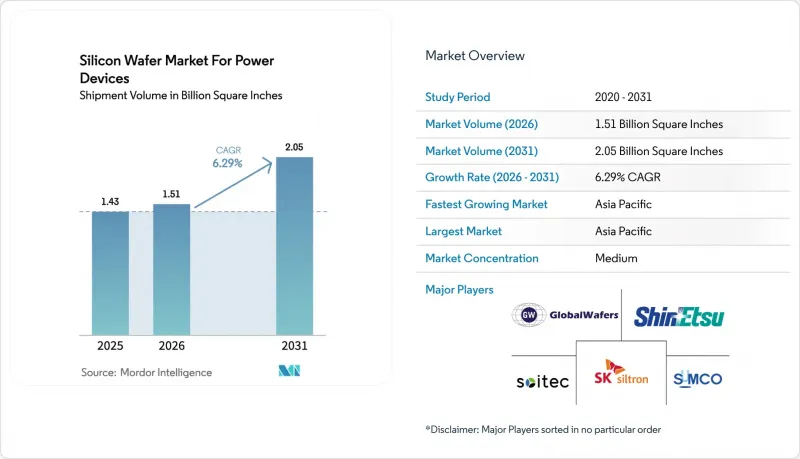
預計到 2025 年,功率元件用矽晶圓市場將達到 14.3 億平方英寸,然後從 2026 年的 15.1 億平方英寸成長到 2031 年的 20.5 億平方英寸,在 2026 年至 2031 年的預測期內,29%。
這一成長主要得益於汽車電氣化、可再生能源電網升級以及工業驅動裝置動力控制從機械控制向電子控制的穩定轉變。寬能隙材料、更嚴格的外延設備出口限制以及大直徑基板的普及正在重塑供應鏈策略,而成本削減的壓力則推動了整合設備製造商的後向整合。矽晶圓市場也受到多晶矽價格波動的影響,這給拋光晶圓的利潤率帶來了壓力,但長期合約緩解了對一級供應商的影響。 300毫米生產線的規模經濟,加上北美和歐洲的在地化獎勵,意味著市場競爭仍然激烈。
功率元件用矽晶圓市場趨勢與展望
電動車的主導了對高效能電力轉換的需求激增。
電動車正從400V電池平台過渡到800V電池平台,將快速充電時間縮短至20分鐘以內,並減輕線束重量。開關頻率超過20kHz的SiC MOSFET正在取代多個矽開關,這使得被動元件得以小型化,並在晶圓價格高昂的情況下降低了逆變器的整體成本。中國、歐洲和美國的汽車製造商正在垂直整合SiC裝置生產,以確保基板供應並進一步提高利潤,這將推動未來幾年晶圓需求的成長。國際能源總署(IEA)預測,到2026年,電池式電動車(BEV)和插電式混合動力汽車(PHEV)的保有量將達到1700萬輛,這將需要約5000萬平方英吋的SiC外延晶圓。這項需求正在支撐整個汽車價值鏈中矽晶圓市場的持續擴張。
可再生能源的擴張正在推動對高壓逆變器所用晶片的需求。
大型太陽能和離岸風力發電發電廠的直流母線電壓為1000至1500伏,這運作功率元件的額定電壓超過1700伏特。預計到2025年,美國太陽能裝置容量將增加35吉瓦,風能裝置容量將增加12吉瓦,這意味著逆變器模組將需要約8,000萬平方英吋的高壓基板。印度等新興市場也緊跟著,每年設定吉瓦級的目標,並強制要求提高逆變器的效率,建議使用碳化矽(SiC)裝置。歐洲的競標現在規定了嚴格的諧波失真閾值,進一步加速了低缺陷密度厚外延晶片的應用。這些政策共同推動了高壓領域矽晶片市場的發展動能。
多晶矽原料價格波動
多晶矽現貨價格從2023年初的每公斤30美元跌至2024年底的每公斤6-8美元,導致拋光晶圓的毛利率下降高達8個百分點。受長期合約限制、價格居高不下的供應商,在現貨買家出價低於自身價格時,會面臨機會成本。針對傾銷的貿易調查加劇了關稅的不確定性,增加了採購風險,並阻礙了短期規劃。雖然外延級供應商可以透過溢價來吸收部分波動,但持續的波動可能會抑制投資意願,並延緩成本敏感型晶圓產能的擴張。
細分市場分析
預計到2025年,200mm規格的矽晶圓仍將佔據功率元件矽晶圓市場62.68%的佔有率。這反映了傳統晶圓廠基礎設施在中功率元件製造方面持續的成本效益。然而,隨著一級汽車供應商要求增加每片晶圓的晶片數量以攤銷潔淨室的固定成本,預計300mm規格的複合年成長率將達到7.56%。初步生產批次顯示,在缺陷密度相當的情況下,可用晶片數量增加了2.3倍,且學習曲線足夠陡峭,足以證明更大直徑的矽晶圓能夠在矽晶圓市場保持其規模經濟優勢。
儘管超過 50µm 的熱機械翹曲導致的良率下降仍然限制了即時的大規模應用,但標準化機構正在推動將厚度偏差目標降低到 2µm 以下。背面離子布植和最佳化的外延製程已實現了兩位數的良率提升,預計四年內將迎來大規模生產的轉捩點。能夠掌握翹曲控制技術的領導企業將在整個矽晶圓市場保持持續的成本優勢。
預計到2025年,外延晶片將佔據64.39%的市場佔有率,年複合成長率達7.16%,主要得益於溝槽柵極MOSFET的普及。精確的摻雜和厚度均勻性能夠降低導通電阻並提高開關速度,這對於汽車和可再生能源動力傳動系統至關重要。沉積設備與人工智慧輔助測量技術的緊密整合,已將設備運轉率從75%提升至85%,釋放了潛在的產能,從而支撐了高階矽晶片市場的強勁成長。
拋光基板在二極體和傳統閘流體中仍然發揮著至關重要的作用。儘管這些領域的價格閾值仍然較低,但多晶矽價格的飆升正給利潤率帶來越來越大的壓力。同時涉足拋光和外延領域的供應商正在有效地降低風險。然而,持續成長的趨勢顯然正在轉向高規格外延技術,這凸顯了其在更廣泛的矽晶圓市場中的戰略重要性。
《功率元件矽晶圓市場報告》按直徑(150毫米以上)、晶圓類型(拋光和外延)、裝置類型(IGBT等)、電壓範圍(低壓、中壓、高壓)、終端應用產業(汽車、工業自動化、可再生能源和儲能等)以及地區進行細分。市場預測以體積(平方英吋)為單位。
區域分析
預計到2025年,亞太地區將佔據69.98%的市場佔有率,並將在2031年之前保持8.01%的複合年成長率。中國國家矽產業集團的擴張計畫、日本對300毫米拋光生產線的投資以及韓國碳化矽產能的提升,共同建構了一個支撐矽晶圓市場的強大生態系統。政府在機器人、電動車和可再生能源領域的發展目標,進一步強化了區域需求,並確保本地晶圓廠保持接近運作。
在北美,受《晶片製造和整合法案》(CHIPS Act)的獎勵以及汽車行業在地化目標的推動,投資正在激增。位於紐約州、北卡羅來納州和德克薩斯的新工廠將減少對進口的依賴,分散供應風險,並在更靠近終端市場的地方建立最先進的300毫米製程。該地區有利的政策環境以及與主要半導體製造設備供應商的便利對接,正使北美成為矽晶圓市場領先的第二大中心。
歐洲正利用《歐洲晶片法案》和嚴格的汽車排放氣體法規來擴大其在全球功率元件生產中的佔有率。在數十億美元公共資金的支持下,德國和義大利的擴建計畫重點在於發展碳化矽外延和300毫米矽晶圓技術。專注於工程基板和超薄晶圓的聯合平台清楚地展現了歐洲的技術差異化策略,而非成本領先策略。儘管南美、中東和非洲仍然嚴重依賴進口,但這些初步舉措表明,歐洲有著建立區域性基板製造能力的長期願景。
其他好處:
- Excel格式的市場預測(ME)表
- 3個月的分析師支持
目錄
第1章:引言
- 研究假設和市場定義
- 調查範圍
第2章:調查方法
第3章執行摘要
第4章 市場狀況
- 市場概覽
- 市場促進因素
- 電動車的主導了對高效能電力轉換的需求激增。
- 可再生能源的擴張正在推動對高壓逆變器所用晶片的需求。
- 過渡到 300 毫米生產線將降低每個晶片的成本。
- 工業自動化水準的提高和智慧工廠的發展是推動這一趨勢的因素。
- 晶圓背面通孔技術可實現超薄汽車模組
- 人工智慧驅動的原位測量技術釋放了外延生產的潛在能力。
- 市場限制因素
- 多晶矽原料價格波動
- 200-300毫米碳化矽晶圓製造廠的資本投資門檻超過10億美元。
- 300mm SiC 晶圓因熱機械翹曲導致良率降低。
- 關於下一代外延反應器出口管制的不確定性
- 產業供應鏈分析
- 監理情勢
- 技術展望
- 宏觀經濟因素對市場的影響
- 波特五力分析
- 新進入者的威脅
- 供應商的議價能力
- 買方的議價能力
- 替代品的威脅
- 競爭公司之間的競爭
第5章 市場規模與成長預測
- 依直徑
- 150 mm
- 200 mm
- 300 mm
- 依晶片類型
- 拋光
- 外延
- 依設備類型
- IGBT
- MOSFET
- 二極體
- 閘流體
- 按電壓範圍
- 低電壓(低於200V)
- 中壓(200-650V)
- 高壓(650V 或更高)
- 按最終用途行業分類
- 車
- 工業自動化
- 可再生能源和儲能
- 家用電源及家用電器
- 通訊和基礎設施用電源系統
- 按地區
- 北美洲
- 美國
- 加拿大
- 墨西哥
- 歐洲
- 德國
- 英國
- 法國
- 其他歐洲地區
- 亞太地區
- 中國
- 日本
- 印度
- 韓國
- 台灣
- 亞太其他地區
- 南美洲
- 中東和非洲
- 北美洲
第6章 競爭情勢
- 市場集中度
- 策略趨勢
- 市佔率分析
- 公司簡介
- Shin-Etsu Chemical
- SUMCO Corporation
- GlobalWafers Co., Ltd.
- Siltronic AG
- SK Siltron Co., Ltd.
- Soitec SA
- National Silicon Industry Group(NSIG)
- Wafer Works Corporation
- Ferrotec Holdings Corporation
- Hangzhou Lion Microelectronics
- Infineon Technologies AG
- STMicroelectronics NV
- onsemi
- Wolfspeed, Inc.
- ROHM Co., Ltd.
- Mitsubishi Electric Corporation
- Fuji Electric Co., Ltd.
- SKC-TankeBlue Semiconductor
- Showa Denko KK
- Hebei Synlight Crystal
第7章 市場機會與未來展望
The silicon wafer market for power devices was valued at 1.43 billion square inches in 2025 and is estimated to grow from 1.51 billion square inches in 2026 to reach 2.05 billion square inches by 2031, at a 6.29% CAGR during the forecast period from 2026 to 2031.
Growth is anchored by vehicle electrification, renewable-energy grid upgrades, and the steady conversion of industrial drives from mechanical to electronic power control. Wide-bandgap materials, tighter export rules on epitaxial tools, and larger-diameter substrates are reshaping supply-chain strategies, while cost-reduction pressure is encouraging backward integration by integrated device manufacturers. The silicon wafer market is further influenced by polysilicon price swings that compress polished-wafer margins, although long-term contracts soften the impact for tier-one suppliers. Competitive intensity remains high as scale advantages in 300 mm lines converge with localization incentives in North America and Europe.
Insights and Trends of Silicon Wafer Market For Power Devices
EV-Led Demand Surge for High-Efficiency Power Conversion
Electric vehicles are shifting from 400-volt to 800-volt battery platforms, cutting fast-charge times to under 20 minutes and reducing wiring mass. SiC MOSFETs switching above 20 kHz replace multiple silicon switches, shrinking passive components and lowering total inverter cost even at a wafer premium. Automakers in China, Europe, and the United States are vertically integrating SiC device production to secure substrate supply and capture additional margin, reinforcing multi-year wafer demand growth. The International Energy Agency projects battery-electric and plug-in hybrid sales of 17 million units in 2026, which equates to roughly 50 million square inches of epitaxial SiC wafers. This demand underpins sustained expansion of the silicon wafer market across the automotive value chain.
Renewable-Energy Build-Out Driving High-Voltage Inverter Wafers
Utility-scale solar and offshore wind installations operate at direct-current bus voltages between 1,000 and 1,500 volts, pushing power-device ratings beyond 1,700 volts. In 2025 the United States added 35 GW of solar and 12 GW of wind capacity, translating into nearly 80 million square inches of high-voltage substrates for inverter modules. Emerging markets such as India are matching this trajectory through multi-gigawatt annual targets, each paired with inverter efficiency mandates that favor SiC devices. European auctions now stipulate stringent harmonic-distortion thresholds, further accelerating the adoption of thick-epi wafers with low defect densities. These policies collectively reinforce the silicon wafer market's momentum in high-voltage segments.
Polysilicon Feedstock Price Volatility
Spot polysilicon prices fell from USD 30 per kg in early 2023 to USD 6-8 per kg by late 2024, compressing polished-wafer gross margins by up to eight percentage points. Suppliers locked into higher long-term contracts faced opportunity costs when spot buyers undercut their pricing. Trade investigations on dumping added tariff uncertainty, raising procurement risk and hindering short-term planning. Although epitaxial-grade suppliers can absorb some variance through premiums, sustained volatility dampens investment appetite and can slow wafer-capacity additions in cost-sensitive segments.
Other drivers and restraints analyzed in the detailed report include:
- Shift to 300 mm Lines Lowering Cost Per Die
- Rising Industrial Automation and Electrified Factory Drives
- USD 1 Billion+ CAPEX Barrier for 200-300 mm SiC Wafer Fabs
For complete list of drivers and restraints, kindly check the Table Of Contents.
Segment Analysis
The 200 mm category retained 62.68% of the silicon wafer market for power devices in 2025, reflecting legacy fab infrastructure that remains cost-effective for medium-power devices. Yet the 300 mm class is forecast to post a 7.56% CAGR as automotive tier-ones demand larger die counts per wafer to amortize clean-room overhead. Early production runs already demonstrate 2.3-times usable die with comparable defect density, confirming that learning curves are steep enough to sustain the silicon wafer market size advantages at larger diameters.
Yield drag from thermo-mechanical bow above 50 µm still limits immediate mass adoption, but standards groups are driving thickness-variation targets below 2 µm. Back-side ion implantation and optimized epitaxy recipes are showing double-digit yield gains, suggesting that volume tipping points will arrive within four years. Scale leaders able to master bow control will hold durable cost positions across the silicon wafer market.
Epitaxial wafers captured 64.39% of the market share in 2025 on the strength of trench-gate MOSFET migration, and they are set to advance at a 7.16% CAGR. Precise doping and thickness uniformity enable lower on-resistance and higher switching speeds, attributes essential to automotive and renewable-energy power trains. Tight integration between deposition tools and AI-assisted metrology now lifts tool utilization from 75% to 85%, freeing latent capacity that underpins a resilient silicon wafer market size at the premium end.
Polished substrates remain relevant in diodes and legacy thyristors, where value thresholds are low but margin pressure is increasing due to polysilicon price shocks. Suppliers operating in both polished and epitaxial segments mitigate risks effectively. However, sustained growth is clearly shifting toward high-specification epitaxy, emphasizing its strategic importance within the broader silicon wafer market.
The Silicon Wafer Market for Power Devices Report is Segmented by Diameter (150 Mm, and More), Wafer Type (Polished, and Epitaxial), Device Type (IGBT, and More), Voltage Range (Low Voltage, Medium Voltage, and High Voltage), End-Use Industry (Automotive, Industrial and Automation, Renewable Energy and Energy Storage, and More), and Geography. The Market Forecasts are Provided in Terms of Volume (Square Inches).
Geography Analysis
Asia-Pacific commanded 69.98% of the market share in 2025 and is projected to post an 8.01% CAGR through 2031. Expansion programs by China's National Silicon Industry Group, Japan's investments in 300 mm polishing lines, and South Korea's SiC capacity additions create a formidable ecosystem that anchors the silicon wafer market. Government robotics, EV, and renewable-energy targets further reinforce regional demand, ensuring that local fabs operate near full utilization.
North America is experiencing an investment surge catalyzed by CHIPS Act incentives and automotive localization goals. New facilities in New York, North Carolina, and Texas reduce dependence on imports, diversify supply risk, and embed advanced 300 mm processes closer to end-markets. The region's policy environment, combined with access to leading semiconductor equipment suppliers, positions it as a credible secondary hub in the silicon wafer market.
Europe leverages the European Chips Act and stringent vehicle-emission rules to claim a larger share of global power-device production. Expansion projects in Germany and Italy emphasize SiC epitaxy and 300 mm silicon, supported by multi-billion-dollar public funding. Collaborative platforms focused on engineered substrates and ultra-thin wafers illustrate Europe's strategy of technology differentiation rather than cost leadership. South America and the Middle East and Africa remain import-oriented today, yet early initiatives signal long-term ambitions to establish regional substrate capabilities.
- Shin-Etsu Chemical
- SUMCO Corporation
- GlobalWafers Co., Ltd.
- Siltronic AG
- SK Siltron Co., Ltd.
- Soitec S.A.
- National Silicon Industry Group (NSIG)
- Wafer Works Corporation
- Ferrotec Holdings Corporation
- Hangzhou Lion Microelectronics
- Infineon Technologies AG
- STMicroelectronics N.V.
- onsemi
- Wolfspeed, Inc.
- ROHM Co., Ltd.
- Mitsubishi Electric Corporation
- Fuji Electric Co., Ltd.
- SKC-TankeBlue Semiconductor
- Showa Denko K.K.
- Hebei Synlight Crystal
Additional Benefits:
- The market estimate (ME) sheet in Excel format
- 3 months of analyst support
TABLE OF CONTENTS
1 INTRODUCTION
- 1.1 Study Assumptions and Market Definition
- 1.2 Scope of the Study
2 RESEARCH METHODOLOGY
3 EXECUTIVE SUMMARY
4 MARKET LANDSCAPE
- 4.1 Market Overview
- 4.2 Market Drivers
- 4.2.1 EV-Led Demand Surge for High-Efficiency Power Conversion
- 4.2.2 Renewable-Energy Build-Out Driving High-Voltage Inverter Wafers
- 4.2.3 Shift to 300 Mm Lines Lowering Cost Per Die
- 4.2.4 Rising Industrial Automation and Electrified Factory Drives
- 4.2.5 On-Wafer Back-Side Vias Enabling Ultra-Thin Automotive Modules
- 4.2.6 AI-Driven In-Situ Metrology Freeing Latent Epi Capacity
- 4.3 Market Restraints
- 4.3.1 Polysilicon Feedstock Price Volatility
- 4.3.2 USD 1 B+ CAPEX Barrier for 200-300 Mm Sic Wafer Fabs
- 4.3.3 Thermo-Mechanical Bow in 300 Mm Sic Wafers Slashing Yields
- 4.3.4 Export-Control Uncertainty for Next-Gen Epi Reactors
- 4.4 Industry Supply-Chain Analysis
- 4.5 Regulatory Landscape
- 4.6 Technological Outlook
- 4.7 Impact of Macroeconomic Factors on the Market
- 4.8 Porter's Five Forces Analysis
- 4.8.1 Threat of New Entrants
- 4.8.2 Bargaining Power of Suppliers
- 4.8.3 Bargaining Power of Buyers
- 4.8.4 Threat of Substitutes
- 4.8.5 Intensity of Competitive Rivalry
5 MARKET SIZE AND GROWTH FORECASTS (VOLUME)
- 5.1 By Diameter
- 5.1.1 150 mm
- 5.1.2 200 mm
- 5.1.3 300 mm
- 5.2 By Wafer Type
- 5.2.1 Polished
- 5.2.2 Epitaxial
- 5.3 By Device Type
- 5.3.1 IGBT
- 5.3.2 MOSFET
- 5.3.3 Diode
- 5.3.4 Thyristor
- 5.4 By Voltage Range
- 5.4.1 Low Voltage (Less than 200V)
- 5.4.2 Medium Voltage (200-650V)
- 5.4.3 High Voltage (Above 650V)
- 5.5 By End-Use Industry
- 5.5.1 Automotive
- 5.5.2 Industrial and Automation
- 5.5.3 Renewable Energy and Energy Storage
- 5.5.4 Consumer and Appliance Power
- 5.5.5 Telecom and Infrastructure Power Systems
- 5.6 By Geography
- 5.6.1 North America
- 5.6.1.1 United States
- 5.6.1.2 Canada
- 5.6.1.3 Mexico
- 5.6.2 Europe
- 5.6.2.1 Germany
- 5.6.2.2 United Kingdom
- 5.6.2.3 France
- 5.6.2.4 Rest of Europe
- 5.6.3 Asia-Pacific
- 5.6.3.1 China
- 5.6.3.2 Japan
- 5.6.3.3 India
- 5.6.3.4 South Korea
- 5.6.3.5 Taiwan
- 5.6.3.6 Rest of Asia-Pacific
- 5.6.4 South America
- 5.6.5 Middle East and Africa
- 5.6.1 North America
6 COMPETITIVE LANDSCAPE
- 6.1 Market Concentration
- 6.2 Strategic Moves
- 6.3 Market Share Analysis
- 6.4 Company Profiles (includes Global level Overview, Market Level Overview, Core Segments, Financials as Available, Strategic Information, Market Rank/Share for Key Companies, Products and Services, and Recent Developments)
- 6.4.1 Shin-Etsu Chemical
- 6.4.2 SUMCO Corporation
- 6.4.3 GlobalWafers Co., Ltd.
- 6.4.4 Siltronic AG
- 6.4.5 SK Siltron Co., Ltd.
- 6.4.6 Soitec S.A.
- 6.4.7 National Silicon Industry Group (NSIG)
- 6.4.8 Wafer Works Corporation
- 6.4.9 Ferrotec Holdings Corporation
- 6.4.10 Hangzhou Lion Microelectronics
- 6.4.11 Infineon Technologies AG
- 6.4.12 STMicroelectronics N.V.
- 6.4.13 onsemi
- 6.4.14 Wolfspeed, Inc.
- 6.4.15 ROHM Co., Ltd.
- 6.4.16 Mitsubishi Electric Corporation
- 6.4.17 Fuji Electric Co., Ltd.
- 6.4.18 SKC-TankeBlue Semiconductor
- 6.4.19 Showa Denko K.K.
- 6.4.20 Hebei Synlight Crystal
7 MARKET OPPORTUNITIES AND FUTURE OUTLOOK
- 7.1 White-space and Unmet-Need Assessment
 矽晶圓市場-全球產業規模、佔有率、趨勢、機會和預測:按晶圓尺寸、類型、應用、最終用戶、地區和競爭格局分類,2021-2031年
 矽晶圓市場規模、佔有率、趨勢和預測:按晶圓尺寸、類型、應用、最終用途和地區分類,2026-2034 年
 半導體矽晶圓回收市場:依回收製程、晶圓類型、晶圓尺寸、應用領域、產業及最終用戶分類-2026-2032年全球市場預測
 2026-2034年全球太陽能矽晶圓市場規模、佔有率、趨勢和成長分析報告
 5G半導體矽晶圓:市場佔有率分析、產業趨勢與統計及成長預測(2026-2031年)工業半導體矽晶圓:市場佔有率分析、產業趨勢與統計、成長預測(2026-2031)高阻矽晶圓:市佔率分析、產業趨勢與統計、成長預測(2026-2031 年)
 2026 年至 2035 年太陽能電池用矽晶圓市場的機會、成長要素、產業趨勢分析與預測。中國半導體矽晶圓市場:市場佔有率分析、產業趨勢與統計及成長預測(2026-2031年)亞太地區半導體矽晶圓:市場佔有率分析、產業趨勢與統計及成長預測(2026-2031)