


 |
市場調查報告書
商品編碼
2044015
5G半導體矽晶圓:市場佔有率分析、產業趨勢與統計及成長預測(2026-2031年)5G Semiconductor Silicon Wafer - Market Share Analysis, Industry Trends & Statistics, Growth Forecasts (2026 - 2031) |
||||||
※ 本網頁內容可能與最新版本有所差異。詳細情況請與我們聯繫。
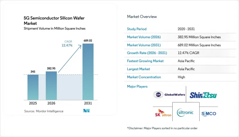
預計 5G 半導體矽晶圓的市場規模將從 2025 年的 3.45 億平方英寸成長到 2026 年的 3.8295 億平方英寸,然後從 2026 年到 2031 年以 12.47% 的複合年成長率,到 2031 年達到 6.920 億平方英寸。
智慧型手機向7奈米以下晶圓的轉變、5G基礎設施在都市區的整合以及向300毫米晶圓的持續過渡,仍然是5G半導體矽晶圓市場結構性成長的主要驅動力。亞太地區行動電話製造商的強勁採購確保了代工廠的長期產量,而北美和歐洲的本土化項目則在不削弱其區域主導地位的前提下,實現了供應區域的多元化。基板供應緊張使得前五名晶圓製造商能夠推動年度價格調整,而近期產業重組,例如斗山收購SK Siltron,進一步增強了現有企業的議價能力。關於使用超純水的環境法規和多晶矽價格的波動抑制了利潤率的擴張,但並未阻礙支撐5G半導體矽晶圓市場成長的資本投資計畫。
全球5G半導體矽晶圓市場趨勢與洞察
5G智慧型手機帶動行動數據流量激增
全球5G終端出貨量預計在2024年達到12億台,並在2026年達到15億台。每台高階終端都依賴7奈米或更小的晶片,這會佔用大量的晶圓面積。像蘋果A18 Pro這樣擁有190億個電晶體的旗艦處理器,需要矽晶圓平整度小於0.3微米,以避免EUV圖形化的缺陷。代工廠提前一年就預訂了300毫米晶圓的產能,這導致基板標價年增12%至15%。客戶正在加速向缺陷密度低於0.01個/平方公分的外延級晶圓過渡,因為一個小於20奈米的顆粒就可能毀掉整個最先進的晶片,從而確保在5G半導體矽晶圓市場獲得高額訂單。
快速部署5G通訊基礎設施
中國計畫在2024年12月前部署420萬個5G基地台,並在2025年底前部署500萬個,在數位基頻向7奈米過渡的同時,對成熟射頻前端節點的需求依然旺盛。歐洲通訊業者利用愛立信整合7奈米ASSP的無線接取網路(RAN)運算系統,加速了小型基地台的部署。這波密集化浪潮使每平方公里所需的基地台數量加倍,推高了對180奈米至7奈米混合製程晶圓的需求。因此,為5G半導體矽晶圓市場供貨的製造商正計劃並行生產過程200毫米和300毫米晶圓,以對沖過程波動風險。
對一家300毫米晶圓廠進行巨額資本投資
新建設的成本在100億至200億美元之間,這使得新進業者寥寥無幾,並強化了支撐定價權的寡頭壟斷格局。 GlobalWafers在德克薩斯州投資75億美元的計畫獲得了美國政府15億美元的津貼,但仍需五年才能獲利。 SUMCO選擇關閉其現有的200毫米生產線,而不是推出。這表明,即使是成熟的公司,如果投資回收期延長,也會退出小規模的資產。因此,產能將以每月5萬片晶圓的速度逐步擴張,限制了5G半導體矽晶圓市場的供應彈性。
細分市場分析
預計到2025年,300mm晶圓的市佔率將達到59.32%,年複合成長率(CAGR)為13.23%,並將在2031年之前維持其主導地位。 300mm晶圓的晶片數量約為200mm晶圓的2.4倍,扣除折舊免稅額後,其單位製造成本降低了30%至35%。亞利桑那州、平壤和愛爾蘭的主要晶圓廠僅生產這種直徑的晶圓,從而確保了穩定的基準需求。因此,在5G半導體矽晶圓市場中,300mm基板的市場規模成長速度將超過其他任何直徑規格。
儘管200毫米晶圓對於傳統的射頻、功率和微機電系統(MEMS)應用仍然至關重要,但資本投資計劃的重心已壓倒性地轉向能夠進行超薄拋光以用於COWS(交叉側基板)的300毫米生產線。能夠保證厚度小於微米且無翹曲的供應商正在獲得高價值契約,而二線製造商則專注於為汽車和工業買家提供穩定的200微米服務。這種兩極化將確保5G半導體矽晶圓市場的長期成長,並減輕經濟波動的影響。
《5G半導體晶圓市場報告》以晶圓直徑(300毫米和200毫米)、技術節點(先進節點、主流節點、成熟節點)、最終用途(智慧型手機、通訊基礎設施、固定無線接入、工業5G)和地區(北美、歐洲、亞太地區及其他地區)進行細分。市場預測以體積(平方英吋)為單位。
區域分析
到2025年,亞太地區將佔據全球5G半導體晶圓市場72.61%的佔有率,並將在2031年之前以13.83%的複合年成長率持續成長。中國420萬個廣域基地台和台灣的晶圓代工產業叢集構成了無可比擬的需求源泉,而日本晶圓供應商則佔據了全球300毫米晶圓產量的一半以上。區域政策,特別是北京的本土化政策和東京的先進封裝補貼計劃,正在進一步鞏固產能,並強化該地區的主導地位。
北美正透過美國《晶片與科學法案》(CHIPS and Science Act)加強其戰略佈局,該法案為德克薩斯州、亞利桑那州、紐約州和俄亥俄州的晶圓廠提供津貼。 2028年,這些設施全面運作後,每年將消耗約3,000萬至3,500萬平方英吋的晶圓,約佔全球市場佔有率的10%。這將確保國內國防和關鍵基礎設施的供應,同時不會顯著削弱亞洲的生產優勢。加拿大和墨西哥正在加速投資配套的後端設備和成熟製程節點,以建構支援5G半導體矽晶圓市場的洲際生態系統。
歐洲的「晶片法案」正在投資430億歐元(約470億美元)新建產能。一旦馬格德堡和德勒斯登的工廠全面運作,預計將推動區域晶圓需求從2025年的8%增加到2030年的12%-14%。儘管南美洲、中東和非洲的總合佔有率目前仍不足3%,但預計成長勢頭強勁,這主要得益於巴西汽車電氣化和阿拉伯聯合大公國資料中心的發展。即使是這些小規模的地區,也在推動5G半導體矽晶圓市場全球覆蓋範圍的擴大。
其他好處:
- Excel格式的市場預測(ME)表
- 3個月的分析師支持
目錄
第1章:引言
- 研究假設和市場定義
- 調查範圍
第2章:調查方法
第3章執行摘要
第4章 市場狀況
- 市場概覽
- 市場促進因素
- 5G智慧型手機帶動行動數據流量激增
- 快速部署5G通訊基礎設施
- 5G設備對先進節點晶片的需求不斷成長
- 採用矽晶圓減薄技術整合5G毫米波天線
- 工業自動化領域專用 5G 網路的發展
- 政府獎勵鼓勵新興國家晶圓製造在地化
- 市場限制因素
- 對300毫米晶圓廠進行大量資本投資
- 半導體級多晶矽供應鏈中斷
- 7nm 以下節點射頻前端積體電路的良率挑戰。
- 限制在晶圓製造中使用超純水的環境法規。
- 產業供應鏈分析
- 監理情勢
- 技術展望
- 宏觀經濟因素對市場的影響
- 波特五力分析
- 新進入者的威脅
- 供應商的議價能力
- 買方的議價能力
- 替代品的威脅
- 競爭公司之間的競爭
第5章 市場規模與成長預測
- 依晶圓直徑
- 300 mm
- 200 mm
- 依技術節點
- 先進節點(小於7奈米)
- 主流製程(10nm 至 28nm)
- 成熟節點(28nm以上)
- 按最終用途
- 智慧型手機
- 通訊基礎設施(大型基地台/小型基地台)
- 固定無線接入(FWA)
- 工業5G
- 按地區
- 北美洲
- 美國
- 加拿大
- 墨西哥
- 歐洲
- 德國
- 英國
- 法國
- 其他歐洲地區
- 亞太地區
- 中國
- 日本
- 印度
- 韓國
- 台灣
- 亞太其他地區
- 南美洲
- 中東和非洲
- 北美洲
第6章 競爭情勢
- 市場集中度
- 策略趨勢
- 市佔率分析
- 公司簡介
- Shin-Etsu Chemical Co., Ltd.
- SUMCO Corporation
- GlobalWafers Co., Ltd.
- Siltronic AG
- SK Siltron Co., Ltd.
- Wafer Works Corporation
- Gritek Electronics Co., Ltd.
- Addison Engineering, Inc.
- Ferrotec Holdings Corporation
- Okmetic Oyj
- LG Electronics Inc.(Wafer Business)
- Taiwan Semiconductor Manufacturing Company Limited
- Samsung Electronics Co., Ltd.
- GlobalFoundries Inc.
- Semiconductor Manufacturing International Corporation
- United Microelectronics Corporation
- Tower Semiconductor Ltd.
- Vanguard International Semiconductor Corporation
- Powerchip Semiconductor Manufacturing Corporation
- onsemi
第7章 市場機會與未來展望
The 5G semiconductor silicon wafer market size is expected to grow from 345 million square inches in 2025 to 382.95 million square inches in 2026, and is forecast to reach 689.02 million square inches by 2031, at a 12.47% CAGR over 2026-2031. Sub-7-nanometer migration across smartphones, densification of urban 5G infrastructure, and sustained conversion to 300-millimeter substrates remain the structural growth engines for the 5G semiconductor silicon wafer market. Strong procurement from Asia-Pacific handset makers secures long-term foundry output, while North American and European onshoring programs diversify geographic supply without displacing the region's dominance. Tight substrate availability enables the top five wafer makers to push annual price escalators, and recent consolidation, such as Doosan's purchase of SK Siltron, intensifies the negotiating leverage of incumbents. Environmental restrictions on ultra-pure water usage and polysilicon price swings temper margin expansion but have not derailed capex programs that underpin the 5G semiconductor silicon wafer market's growth trajectory.
Global 5G Semiconductor Silicon Wafer Market Trends and Insights
Surging Mobile Data Traffic from 5G Smartphones
Global 5G handset shipments reached 1.2 billion in 2024 and are forecast to hit 1.5 billion by 2026, each premium device relying on sub-7 nanometer dies that consume materially larger wafer area. Flagship processors, such as Apple's A18 Pro with 19 billion transistors, demand silicon flatness below 0.3 micrometers to avoid EUV patterning defects. Foundries pre-book 300 millimeter capacity up to a year ahead, pushing substrate list prices 12%-15% higher year-on-year. Because a single sub-20 nanometer particle can kill an entire advanced die, customers increasingly shift to epitaxial-quality wafers with <0.01 defects per cm2, locking in premium contracts for the 5G semiconductor silicon wafer market.
Rapid Deployment of 5G Telecom Infrastructure
China installed 4.2 million 5G base stations by December 2024 and targets 5 million by end-2025, retaining mature-node demand for RF front-ends while digital baseband moves to 7 nanometers. European operators accelerated small-cell rollouts using Ericsson's RAN Compute systems that integrate 7 nanometer ASSPs. The densification wave multiplies required sites per square kilometer, lifting mixed-node wafer demand spanning 180 nanometers to 7 nanometers. Suppliers serving the 5G semiconductor silicon wafer market, therefore, schedule overlapping 200 millimeter and 300 millimeter production runs to hedge node volatility.
High Capital Expenditure for 300 mm Wafer Fabs
Building a greenfield 300 millimeter plant costs USD 10 billion-USD 20 billion, keeping new entry rare and reinforcing the oligopoly that underpins pricing power. GlobalWafers' USD 7.5 billion Texas project received USD 1.5 billion in U.S. grants, yet still faces a five-year ramp before revenue begins. SUMCO elected to close a legacy 200 millimeter line rather than reinvest, signaling that even incumbents exit sub-scale assets when payback periods lengthen. Resulting capacity staging in 50,000-wafer-per-month increments limits supply elasticity for the 5G semiconductor silicon wafer market.
Other drivers and restraints analyzed in the detailed report include:
- Increasing Demand for Advanced Node Chips in 5G Devices
- Adoption of Silicon Wafer Thinning for 5G mmWave Antenna Integration
- Supply Chain Disruptions of Semiconductor Grade Polysilicon
For complete list of drivers and restraints, kindly check the Table Of Contents.
Segment Analysis
The 300 millimeter category held 59.32% of the market share in 2025 and benefits from a 13.23% CAGR, cementing its primacy through 2031. Each 300-millimeter wafer yields roughly 2.4X the die count of a 200-millimeter wafer, translating to 30%-35% lower unit fabrication cost once depreciation is absorbed. Leading fabs in Arizona, Pyeongtaek, and Ireland process only this diameter, ensuring locked-in baseline demand. The 5G semiconductor silicon wafer market size for 300 millimeter substrates will therefore scale faster than any other diameter set.
Although 200 millimeters remains indispensable for legacy RF, power, and MEMS, capital plans heavily favor 300 millimeter lines capable of ultra-thin grinding for chip-on-wafer-on-substrate packaging. Suppliers able to guarantee warp-free thinning below 50 micrometers capture premium contracts, while second-tier producers focus on stabilizing 200-micrometer service for automotive and industrial buyers. This bifurcation secures long-run growth and cushions cyclicality within the broader 5G semiconductor silicon wafer market.
The 5G Semiconductor Silicon Wafer Market Report is Segmented by Wafer Diameter (300 Mm and 200 Mm), Technology Node (Advanced Node, Mainstream Node, and Mature Node), End Application (Smartphones, Telecom Infrastructure, Fixed Wireless Access, and Industrial 5G), and Geography (North America, Europe, Asia-Pacific, and More). The Market Forecasts are Provided in Terms of Volume (Square Inches).
Geography Analysis
Asia-Pacific controlled 72.61% of the 5G semiconductor silicon wafer market in 2025 and expands at 13.83% CAGR through 2031. China's 4.2 million macro base stations and Taiwan's foundry cluster together generate unrivaled demand pools, while Japanese wafer suppliers command more than half of global 300 millimeter output. Regional policy, notably Beijing's localization mandates and Tokyo's advanced packaging subsidies, further anchors capacity and reinforces the region's leadership position.
North America captures strategic mindshare through the U.S. CHIPS and Science Act, which subsidizes fabs in Texas, Arizona, New York, and Ohio. Once fully online by 2028, these sites will consume roughly 30-35 million square inches annually about 10% global share securing domestic supply for defense and critical infrastructure without materially eroding Asia's volume lead. Canada and Mexico accelerate complimentary back-end and mature-node investments, rounding out a continental ecosystem that supports the 5G semiconductor silicon wafer market.
Europe's Chips Act channels EUR 43 billion (USD 47 billion) into new capacity, lifting regional wafer demand from 8% in 2025 toward an expected 12%-14% by 2030 once sites in Magdeburg and Dresden ramp. South America and the Middle East and Africa jointly remain below 3% share, with growth tied to automotive electrification in Brazil and data-center deployments in the United Arab Emirates. These smaller regions nonetheless widen the global footprint of the 5G semiconductor silicon wafer market.
List of Companies Covered in this Report:
- Shin-Etsu Chemical Co., Ltd.
- SUMCO Corporation
- GlobalWafers Co., Ltd.
- Siltronic AG
- SK Siltron Co., Ltd.
- Wafer Works Corporation
- Gritek Electronics Co., Ltd.
- Addison Engineering, Inc.
- Ferrotec Holdings Corporation
- Okmetic Oyj
- LG Electronics Inc. (Wafer Business)
- Taiwan Semiconductor Manufacturing Company Limited
- Samsung Electronics Co., Ltd.
- GlobalFoundries Inc.
- Semiconductor Manufacturing International Corporation
- United Microelectronics Corporation
- Tower Semiconductor Ltd.
- Vanguard International Semiconductor Corporation
- Powerchip Semiconductor Manufacturing Corporation
- onsemi
Additional Benefits:
- The market estimate (ME) sheet in Excel format
- 3 months of analyst support
TABLE OF CONTENTS
1 INTRODUCTION
- 1.1 Study Assumptions and Market Definition
- 1.2 Scope of the Study
2 RESEARCH METHODOLOGY
3 EXECUTIVE SUMMARY
4 MARKET LANDSCAPE
- 4.1 Market Overview
- 4.2 Market Drivers
- 4.2.1 Surging Mobile Data Traffic from 5G Smartphones
- 4.2.2 Rapid Deployment of 5G Telecom Infrastructure
- 4.2.3 Increasing Demand for Advanced Node Chips in 5G Devices
- 4.2.4 Adoption of Silicon Wafer Thinning for 5G mmWave Antenna Integration
- 4.2.5 Growth of Private 5G Networks in Industrial Automation
- 4.2.6 Government Incentives for Localized Wafer Fabrication in Emerging Economies
- 4.3 Market Restraints
- 4.3.1 High Capital Expenditure for 300 mm Wafer Fabs
- 4.3.2 Supply Chain Disruptions of Semiconductor Grade Polysilicon
- 4.3.3 Yield Challenges at <7nm Nodes for RF Front-End ICs
- 4.3.4 Environmental Regulations Limiting Ultra-Pure Water Usage in Wafer Production
- 4.4 Industry Supply-Chain Analysis
- 4.5 Regulatory Landscape
- 4.6 Technological Outlook
- 4.7 Impact of Macroeconomic Factors on the Market
- 4.8 Porter's Five Forces Analysis
- 4.8.1 Threat of New Entrants
- 4.8.2 Bargaining Power of Suppliers
- 4.8.3 Bargaining Power of Buyers
- 4.8.4 Threat of Substitutes
- 4.8.5 Intensity of Competitive Rivalry
5 MARKET SIZE AND GROWTH FORECASTS (VOLUME)
- 5.1 By Wafer Diameter
- 5.1.1 300 mm
- 5.1.2 200 mm
- 5.2 By Technology Node
- 5.2.1 Advanced Node (Below 7nm)
- 5.2.2 Mainstream Node (10nm-28nm)
- 5.2.3 Mature Node (Above 28nm)
- 5.3 By End Application
- 5.3.1 Smartphones
- 5.3.2 Telecom Infrastructure (Macro / Small Cells)
- 5.3.3 Fixed Wireless Access (FWA)
- 5.3.4 Industrial 5G
- 5.4 By Geography
- 5.4.1 North America
- 5.4.1.1 United States
- 5.4.1.2 Canada
- 5.4.1.3 Mexico
- 5.4.2 Europe
- 5.4.2.1 Germany
- 5.4.2.2 United Kingdom
- 5.4.2.3 France
- 5.4.2.4 Rest of Europe
- 5.4.3 Asia-Pacific
- 5.4.3.1 China
- 5.4.3.2 Japan
- 5.4.3.3 India
- 5.4.3.4 South Korea
- 5.4.3.5 Taiwan
- 5.4.3.6 Rest of Asia-Pacific
- 5.4.4 South America
- 5.4.5 Middle East and Africa
- 5.4.1 North America
6 COMPETITIVE LANDSCAPE
- 6.1 Market Concentration
- 6.2 Strategic Moves
- 6.3 Market Share Analysis
- 6.4 Company Profiles (includes Global level Overview, Market Level Overview, Core Segments, Financials as Available, Strategic Information, Market Rank/Share for Key Companies, Products and Services, and Recent Developments)
- 6.4.1 Shin-Etsu Chemical Co., Ltd.
- 6.4.2 SUMCO Corporation
- 6.4.3 GlobalWafers Co., Ltd.
- 6.4.4 Siltronic AG
- 6.4.5 SK Siltron Co., Ltd.
- 6.4.6 Wafer Works Corporation
- 6.4.7 Gritek Electronics Co., Ltd.
- 6.4.8 Addison Engineering, Inc.
- 6.4.9 Ferrotec Holdings Corporation
- 6.4.10 Okmetic Oyj
- 6.4.11 LG Electronics Inc. (Wafer Business)
- 6.4.12 Taiwan Semiconductor Manufacturing Company Limited
- 6.4.13 Samsung Electronics Co., Ltd.
- 6.4.14 GlobalFoundries Inc.
- 6.4.15 Semiconductor Manufacturing International Corporation
- 6.4.16 United Microelectronics Corporation
- 6.4.17 Tower Semiconductor Ltd.
- 6.4.18 Vanguard International Semiconductor Corporation
- 6.4.19 Powerchip Semiconductor Manufacturing Corporation
- 6.4.20 onsemi
7 MARKET OPPORTUNITIES AND FUTURE OUTLOOK
- 7.1 White-Space and Unmet-Need Assessment
 矽晶圓市場-全球產業規模、佔有率、趨勢、機會和預測:按晶圓尺寸、類型、應用、最終用戶、地區和競爭格局分類,2021-2031年
 矽晶圓市場規模、佔有率、趨勢和預測:按晶圓尺寸、類型、應用、最終用途和地區分類,2026-2034 年
 半導體矽晶圓回收市場:依回收製程、晶圓類型、晶圓尺寸、應用領域、產業及最終用戶分類-2026-2032年全球市場預測
 2026-2034年全球太陽能矽晶圓市場規模、佔有率、趨勢和成長分析報告
 工業半導體矽晶圓:市場佔有率分析、產業趨勢與統計、成長預測(2026-2031)用於功率元件的矽晶圓:市場佔有率分析、行業趨勢和統計數據以及成長預測(2026-2031 年)高阻矽晶圓:市佔率分析、產業趨勢與統計、成長預測(2026-2031 年)
 2026 年至 2035 年太陽能電池用矽晶圓市場的機會、成長要素、產業趨勢分析與預測。中國半導體矽晶圓市場:市場佔有率分析、產業趨勢與統計及成長預測(2026-2031年)亞太地區半導體矽晶圓:市場佔有率分析、產業趨勢與統計及成長預測(2026-2031)