


 |
市場調查報告書
商品編碼
2044013
高阻矽晶圓:市佔率分析、產業趨勢與統計、成長預測(2026-2031 年)High-Resistivity Silicon Wafer - Market Share Analysis, Industry Trends & Statistics, Growth Forecasts (2026 - 2031) |
||||||
※ 本網頁內容可能與最新版本有所差異。詳細情況請與我們聯繫。
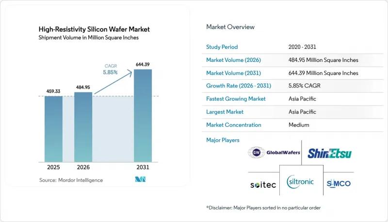
高阻矽晶片市場預計將從 2025 年的 4.5933 億平方英寸成長到 2026 年的 4.8495 億平方英寸,到 2031 年達到 6.4439 億平方英寸,2026 年至 2031 年的複合年成長率為 5.85%。
部署5G宏基地台和小型基地台的通訊業者已簽署多年期射頻SOI開關和功率放大器採購協議,確保了即使行動電話終端出貨量放緩,基本需求仍然存在。隨著歐洲和中國強制要求配備L2級及以上駕駛輔助功能,每輛車的雷達數量不斷增加,每個新增感測器都需要電阻率超過1000歐姆/公分的基板。光子積體電路供應商目前正在認證300毫米高電阻平台,晶圓尺寸也正向更大直徑的方向發展。最後,美國、歐洲和日本的政府獎勵正在加速國內產能的擴張,從而保護買家免受地緣政治因素造成的供應衝擊。
全球高阻矽晶圓市場趨勢及洞察
5G智慧型手機中射頻SOI技術的廣泛應用
目前,所有5G設備均配備射頻SOI前端電路,為高阻矽晶圓市場創造了穩固的結構性需求。 HR-SOI富含陷阱的層能夠抑制2GHz以上頻率的基板耦合,使功率放大器無需外部濾波器即可達到線性度目標。預計每部智慧型手機的組件價值將從2020年的1.20美元增至2024年的2.10美元,設計人員已鎖定200mm晶圓的產能直至2027年。儘管設備出貨量趨於平穩,但隨著印度、東南亞和南美洲等地區6GHz以下頻段覆蓋範圍的擴大,晶圓需求依然強勁。
汽車雷達生產規模擴大
歐盟2024年安全法規強制要求每輛新車安裝多個77-81 GHz雷達,將導致歐洲和北美高阻矽晶圓的需求增加。與77 GHz體矽CMOS相比,基於高阻SOI(高阻SOI)的矽雷達可將相位雜訊降低15%,從而支援高級駕駛輔助系統(ADAS)。隨著中國2025年新車安全評鑑協會(NCAP)標準日益嚴格,國內品牌擴大採用側後雷達,預計這將推動未來十年基板市場達到兩位數成長。
製造無缺陷的300毫米高阻晶圓的複雜性
300mmFloat-Zone晶體生長需要嚴格的溫度控管,導致其初始良率比 200mm 同等尺寸的晶圓低 20 個百分點。確保整個 300mm 高分辨 SOI 晶圓的外延均勻性在 ±2nm 以內仍然是一項挑戰,延緩了客戶的認證流程。新建生產線的成本在 8 億至 12 億美元之間,阻礙了新進入者,導致供應緊張,現貨價格持續上漲,直到工藝成熟。
細分市場分析
截至2025年,200mm晶圓將佔據高阻矽晶圓市場54.68%的佔有率,這反映了2010年代建成的射頻積體電路晶圓廠的部署。由於開關和低雜訊放大器所需的晶片尺寸仍然很小,Qorvo和Skyworks等領先的前端供應商仍在運作成熟的200mm生產線。然而,一旦良率穩定,300mm晶圓廠可望降低單晶片成本,預計早期採用者將在2025年底前實現85%的良率,從而縮小與200mm製程的差距。儘管每座晶圓廠近10億美元的資本投資成本正在減緩這一轉型進程,但由於其能夠將射頻、基頻和人工智慧加速器整合到單一晶片上,更大的晶圓尺寸仍然具有經濟吸引力。
展望未來,300mm晶圓市場預計將以每年6.74%的速度成長,逐步削弱200mm晶圓在高阻矽晶圓市場的主導地位。整合數位訊號處理的汽車雷達積體電路將成為引領這一趨勢的先鋒產品,因為通道數量的增加將導致晶片面積超過120mm²。雖然150mm基板仍在一些傳統的軍事項目中使用,但其絕對產量正在下降。隨著良率學習的不斷深入以及德克薩斯、弗賴貝格和龜尾等地的補貼產能擴張持續進行,300mm晶圓在射頻元件量產方面的經濟優勢將變得顯而易見。
到2025年,拋光高阻矽將佔據38.86%的市場佔有率,因為在成像感測器和工業檢測器中,低暗電流的重要性將超過射頻隔離。外延晶片支援功率元件和微機電系統(MEMS),其中低摻雜外延層可提供電壓隔離和機械優勢。然而,隨著5G、Wi-Fi 7和相位陣列雷達對更高線性度的需求,預計高阻SOI(HR-SOI)將以6.48%的複合年成長率成長。 RFeSI-3平台可將諧波失真降低2 dB,這使得HR-SOI成為26 dBm功率放大器的關鍵材料。
隨著 GlobalFoundries、台積電和其他代工廠推進 300mm 晶圓的 HR-SOI 認證,其應用正在加速,有效提高了每片晶圓的有效晶片數量,同時降低了成本成長。因此,用於 HR-SOI基板的高阻矽晶圓市場規模預計將比整體市場成長更快。供應集中度是一把雙面刃。雖然 Soytech 60% 的市場佔有率確保了品質穩定性,但也可能導致整個生態系統面臨單一故障點的風險,從而促使一級 IC 製造商盡可能從信越化學和 SUMCO 兩家供應商採購。
《高阻矽晶圓市場報告》依晶圓直徑(150毫米、200毫米、300毫米)、晶圓類型(拋光、外延、高阻SOI)、裝置應用(射頻前端元件、毫米波和5G收發器IC、汽車雷達IC等)、最終用戶(家用電子電器、工業、汽車等)和地區細分。市場預測以體積(平方英吋)為單位。
區域分析
預計到2025年,亞太地區將以58.89%的市佔率主導高阻矽晶圓市場,並有望在2031年之前以6.98%的年均複合成長率持續成長。日本信越化學和SUMCO兩家公司共同佔據全球一半的Float-Zone熔煉產能,而台灣的無晶圓射頻企業則將這些晶圓加工成功率放大器並出口到世界各地。中國正積極投資Float-Zone產能的在地化,以降低對進口的依賴,並提供比同類日本產品便宜20-30%的晶圓。韓國SK Siltron正在擴大其300毫米晶圓的量產能力,以滿足汽車雷達供應商分散在各地的需求。
在北美,由於《晶片製造和整合法案》(CHIPS Act)提供的補貼,產能正以前所未有的速度擴張。該法案為特種晶圓工廠提供了高達40%的資本投資補貼。 GlobalWafers公司已在德克薩斯州啟動建設,並獲得了4億美元的聯邦撥款,計劃於2027年交付首批晶圓。這些新生產線將優先生產用於國內射頻積體電路(RF-IC)和汽車市場的300毫米高解析度SOI晶圓,旨在縮短前置作業時間並降低貿易風險。歐洲也在走類似的道路。在獲得3億歐元(約3.25億美元)撥款的支持下,Siltronic公司位於弗賴貝格的工廠擴建項目正在推進,該地區對進口的依賴程度正在降低,並更有能力支持汽車雷達生態系統的發展。
儘管南美、中東和非洲的需求仍處於早期階段,但政策舉措可望擴大其規模。巴西正在進口採用高阻矽的射頻前端,用於其最初的5G部署;而阿拉伯聯合大公國則正在考慮建造具備專業晶圓製造能力的新晶圓廠。目前非洲的採用率很低,但南非的汽車產業正在縮小技術差距,未來將需要雷達積體電路,進而需要高阻基板。這些地區在2031年之前貢獻較小,但在未來十年將成為多元化發展的選擇。
其他好處:
- Excel格式的市場預測(ME)表
- 3個月的分析師支持
目錄
第1章:引言
- 研究假設和市場定義
- 調查範圍
第2章:調查方法
第3章執行摘要
第4章 市場狀況
- 市場概覽
- 市場促進因素
- 5G智慧型手機中射頻SOI技術的廣泛應用
- 汽車雷達生產規模擴大
- 衛星通訊對毫米波矽的需求不斷成長
- 將自適應波束成形技術整合到相位陣列天線中
- 利用高阻基板開發光子積體電路
- 政府對國內半導體製造的獎勵
- 市場限制因素
- 製造無缺陷的300毫米高阻晶圓的複雜性
- 與傳統矽晶片相比,價格溢價
- 超高純度Float-Zone矽油的供應限制
- 用於射頻和功率元件的新型GaN和SiC基板
- 產業供應鏈分析
- 監理情勢
- 技術展望
- 宏觀經濟因素對市場的影響
- 波特五力分析
- 新進入者的威脅
- 供應商的議價能力
- 買方的議價能力
- 替代品的威脅
- 競爭公司之間的競爭
第5章 市場規模與成長預測
- 依晶圓直徑
- 150 mm
- 200 mm
- 300 mm
- 依晶片類型
- 拋光高阻矽
- 外延高阻矽
- 高電阻絕緣體上矽(HR-SOI)
- 裝置應用程式
- 射頻前端元件(功率放大器、開關、低雜訊放大器)
- 毫米波和5G收發器積體電路
- 汽車雷達積體電路(77-81 GHz)
- 檢測器和成像裝置
- 微機電系統和先進感測器積體電路
- 最終用戶
- 家用電子產品
- 工業的
- 溝通
- 車
- 其他終端用戶應用程式
- 按地區
- 北美洲
- 美國
- 加拿大
- 墨西哥
- 歐洲
- 德國
- 英國
- 法國
- 其他歐洲地區
- 亞太地區
- 中國
- 日本
- 印度
- 韓國
- 亞太其他地區
- 南美洲
- 中東和非洲
- 北美洲
第6章 競爭情勢
- 市場集中度
- 策略趨勢
- 市佔率分析
- 公司簡介
- Shin-Etsu Handotai Co., Ltd.
- SUMCO Corporation
- Siltronic AG
- GlobalWafers Co., Ltd.
- Soitec SA
- Okmetic Oyj
- Wafer Works Corp.
- SK Siltron Co., Ltd.
- Zhejiang Ferrotec Semiconductor Co., Ltd.
- Addison Engineering, Inc.
- Topsil Semiconductor Materials A/S
- SINO-American Silicon Products Inc.
- Wafer World Inc.
- Virginia Semiconductor, Inc.
- Shanghai Simgui Technology Co., Ltd.
- Nova Electronic Materials, LLC
- Ferrotec Holdings Corporation
- pSemi Corporation
第7章 市場機會與未來展望
The high-resistivity silicon wafer market size is expected to increase from 459.33 million square inches in 2025 to 484.95 million square inches in 2026 and reach 644.39 million square inches by 2031, growing at a CAGR of 5.85% over 2026-2031.
Operators rolling out 5G macro and small-cell sites have locked in multi-year purchases of RF-SOI switches and power amplifiers, guaranteeing baseline demand even as handset unit growth slows. Radar content per car is rising because Level 2+ assistance features are becoming mandatory in Europe and China, and each additional sensor requires substrates with resistivity above 1,000 ohm-cm. Photonic integrated-circuit vendors are now qualifying 300 mm high-resistivity platforms, shifting the wafer mix toward larger diameters. Finally, government incentives in the United States, Europe, and Japan are accelerating domestic capacity additions, cushioning buyers against geopolitical supply shocks.
Global High-Resistivity Silicon Wafer Market Trends and Insights
Growing Adoption of RF SOI in 5G Smartphones
Every 5G handset now ships with RF-SOI front-end circuitry, cementing a structural pull on the high-resistivity silicon wafer market. The trap-rich layer in HR-SOI limits substrate coupling above 2 GHz, letting power amplifiers meet linearity targets without external filters. Component value per phone climbed from USD 1.20 in 2020 to USD 2.10 in 2024, and designers have already reserved 200 mm capacity through 2027. As sub-6 GHz coverage broadens across India, South-East Asia, and South America, wafer demand remains resilient despite plateauing handset units.
Expansion of Automotive Radar Production
The European Union's 2024 safety regulation mandates multiple 77-81 GHz radars per new vehicle, elevating high-resistivity wafer consumption in Europe and North America. Silicon-based radar on HR-SOI delivers 15% lower phase noise than bulk CMOS at 77 GHz, supporting advanced driver-assistance functions. As China's NCAP tightens in 2025, domestic brands are adding corner and rear radar, driving double-digit substrate growth through the decade.
Complexities in Producing Defect-Free 300 mm HR Wafers
Float-zone crystal growth at 300 mm demands stringent thermal control, and initial yields trail 200 mm equivalents by up to 20 percentage points. Epitaxial uniformity within +-2 nm across a 300 mm HR-SOI wafer remains challenging, slowing customer qualifications. The USD 800 million-USD 1.2 billion price tag for a greenfield line deters new entrants, keeping supply tight and inflating spot prices until processes mature.
Other drivers and restraints analyzed in the detailed report include:
- Rising Demand for mmWave Silicon for Satellite Communications
- Integration of Adaptive Beamforming in Phased-Array Antennas
- Price Premium over Conventional Silicon Wafers
For complete list of drivers and restraints, kindly check the Table Of Contents.
Segment Analysis
The 200 mm segment held 54.68% of the high-resistivity silicon wafer market share in 2025, reflecting the installed base of RF-IC fabs built during the 2010s. Leading front-end vendors such as Qorvo and Skyworks continue to run mature 200 mm lines because die sizes for switches and low-noise amplifiers remain small. However, 300 mm fabs promise lower cost per die once yields stabilize, and early adopters saw an 85% yield by late 2025, narrowing the gap with 200 mm processes. Capital costs near USD 1 billion per facility slow the migration, yet the convergence of RF, baseband, and AI accelerators on a single die makes the larger format economically compelling.
Looking forward, the 300 mm segment is expected to grow at a 6.74% rate, gradually eroding the dominance of 200 mm in the high-resistivity silicon wafer market. Automotive radar ICs integrating digital signal processing will be among the first movers because rising channel counts drive die area beyond 120 mm2. While 150 mm substrates linger in legacy military programs, their absolute volumes are shrinking. As yield learning improves and subsidy-backed capacity ramps in Texas, Freiberg, and Gumi, 300 mm economics will turn decisively favorable for high-volume RF devices.
Polished high-resistivity silicon captured 38.86% of the market share in 2025, thanks to imaging sensors and industrial detectors that value low dark current over RF isolation. Epitaxial wafers support power devices and MEMS, where a lightly doped epi-layer offers voltage blocking or mechanical benefits. HR-SOI, however, is forecast to rise at a 6.48% CAGR as 5G, Wi-Fi 7, and phased-array radars demand enhanced linearity. The RFeSI-3 platform reduced harmonic distortion by 2 dB, making HR-SOI indispensable for 26 dBm power amplifiers.
Adoption accelerates as GlobalFoundries, TSMC, and other foundries qualify HR-SOI at 300 mm, effectively doubling usable die per wafer and shrinking cost penalties. The high-resistivity silicon wafer market size for HR-SOI substrates is therefore set to expand more quickly than the total market volume. Supply concentration remains a double-edged sword: Soitec's 60% share offers stable quality but exposes the ecosystem to single-point failures, prompting tier-1 IC houses to dual-source from Shin-Etsu and SUMCO where possible.
The High-Resistivity Silicon Wafer Market Report is Segmented by Wafer Diameter (150 Mm, 200 Mm, and 300 Mm), Wafer Type (Polished, Epitaxial, and HR-SOI), Device Application (RF Front-End Devices, Mmwave and 5G Transceiver ICs, Automotive Radar ICs, and More), End-User (Consumer Electronics, Industrial, Automotive, and More ), and Geography. The Market Forecasts are Provided in Terms of Volume (Square Inches).
Geography Analysis
Asia-Pacific dominated the high-resistivity silicon wafer market with 58.89% market share in 2025, and is projected to grow at 6.98% through 2031. Japan's Shin-Etsu and SUMCO jointly supply half the world's float-zone capacity, while Taiwan's fabless RF community converts those substrates into power amplifiers exported globally. China is investing aggressively to localize float-zone production, reducing import dependence and offering wafers 20-30% cheaper than Japanese equivalents. South Korea's SK Siltron is ramping 300 mm qualification to serve automotive radar suppliers seeking geographic diversity.
North America is adding capacity faster than historical trends because the CHIPS Act covers up to 40% of capital expenditures for specialty wafer plants. GlobalWafers broke ground in Texas with USD 400 million in federal grants, and first wafers are slated for 2027. These new lines will prioritize 300 mm HR-SOI for domestic RF-IC and automotive markets, shortening lead times and mitigating trade risks. Europe follows a similar path; Siltronic's Freiberg expansion, backed by EUR 300 million (USD 325 million) in subsidies, positions the region to support its automotive radar ecosystem without relying solely on imports.
South America and the Middle East and Africa remain nascent consumers, but policy initiatives could unlock incremental demand. Brazil's initial 5G rollout is importing RF front-ends that incorporate high-resistivity silicon, while the United Arab Emirates is studying a greenfield fab that would include specialty wafer capability. African uptake is negligible today, yet South Africa's automotive sector is narrowing technology gaps that will eventually require radar ICs and, by extension, HR substrates. Although these regions contribute minimally before 2031, they represent diversification options in the next decade.
- Shin-Etsu Handotai Co., Ltd.
- SUMCO Corporation
- Siltronic AG
- GlobalWafers Co., Ltd.
- Soitec S.A.
- Okmetic Oyj
- Wafer Works Corp.
- SK Siltron Co., Ltd.
- Zhejiang Ferrotec Semiconductor Co., Ltd.
- Addison Engineering, Inc.
- Topsil Semiconductor Materials A/S
- SINO-American Silicon Products Inc.
- Wafer World Inc.
- Virginia Semiconductor, Inc.
- Shanghai Simgui Technology Co., Ltd.
- Nova Electronic Materials, LLC
- Ferrotec Holdings Corporation
- pSemi Corporation
Additional Benefits:
- The market estimate (ME) sheet in Excel format
- 3 months of analyst support
TABLE OF CONTENTS
1 INTRODUCTION
- 1.1 Study Assumptions and Market Definition
- 1.2 Scope of the Study
2 RESEARCH METHODOLOGY
3 EXECUTIVE SUMMARY
4 MARKET LANDSCAPE
- 4.1 Market Overview
- 4.2 Market Drivers
- 4.2.1 Growing Adoption of RF SOI in 5G Smartphones
- 4.2.2 Expansion of Automotive Radar Production
- 4.2.3 Rising Demand for mmWave Silicon for Satellite Communications
- 4.2.4 Integration of Adaptive Beamforming in Phased-Array Antennas
- 4.2.5 Development of Photonic ICs on High-Resistivity Substrates
- 4.2.6 Government Incentives for On-shore Semiconductor Manufacturing
- 4.3 Market Restraints
- 4.3.1 Complexities in Producing Defect-Free 300 mm HR Wafers
- 4.3.2 Price Premium over Conventional Silicon Wafers
- 4.3.3 Supply Constraints of Ultra-High-Purity Float-Zone Silicon
- 4.3.4 Emerging GaN and SiC Substrates for RF and Power Devices
- 4.4 Industry Supply-Chain Analysis
- 4.5 Regulatory Landscape
- 4.6 Technological Outlook
- 4.7 Impact of Macroeconomic Factors on the Market
- 4.8 Porter's Five Forces Analysis
- 4.8.1 Threat of New Entrants
- 4.8.2 Bargaining Power of Suppliers
- 4.8.3 Bargaining Power of Buyers
- 4.8.4 Threat of Substitutes
- 4.8.5 Intensity of Competitive Rivalry
5 MARKET SIZE AND GROWTH FORECASTS (VOLUME)
- 5.1 By Wafer Diameter
- 5.1.1 150 mm
- 5.1.2 200 mm
- 5.1.3 300 mm
- 5.2 By Wafer Type
- 5.2.1 Polished High-Resistivity Silicon
- 5.2.2 Epitaxial High-Resistivity Silicon
- 5.2.3 High-Resistivity Silicon-on-Insulator (HR-SOI)
- 5.3 By Device Application
- 5.3.1 RF Front-End Devices (PA, Switches, LNAs)
- 5.3.2 mmWave and 5G Transceiver ICs
- 5.3.3 Automotive Radar ICs (77-81 GHz)
- 5.3.4 Photodetectors and Imaging Devices
- 5.3.5 MEMS and Advanced Sensor ICs
- 5.4 By End-user
- 5.4.1 Consumer Electronics
- 5.4.2 Industrial
- 5.4.3 Telecommunications
- 5.4.4 Automotive
- 5.4.5 Other End-user Applications
- 5.5 By Geography
- 5.5.1 North America
- 5.5.1.1 United States
- 5.5.1.2 Canada
- 5.5.1.3 Mexico
- 5.5.2 Europe
- 5.5.2.1 Germany
- 5.5.2.2 United Kingdom
- 5.5.2.3 France
- 5.5.2.4 Rest of Europe
- 5.5.3 Asia-Pacific
- 5.5.3.1 China
- 5.5.3.2 Japan
- 5.5.3.3 India
- 5.5.3.4 South Korea
- 5.5.3.5 Rest of Asia-Pacific
- 5.5.4 South America
- 5.5.5 Middle East and Africa
- 5.5.1 North America
6 COMPETITIVE LANDSCAPE
- 6.1 Market Concentration
- 6.2 Strategic Moves
- 6.3 Market Share Analysis
- 6.4 Company Profiles (includes Global level Overview, Market Level Overview, Core Segments, Financials as Available, Strategic Information, Market Rank/Share for Key Companies, Products and Services, and Recent Developments)
- 6.4.1 Shin-Etsu Handotai Co., Ltd.
- 6.4.2 SUMCO Corporation
- 6.4.3 Siltronic AG
- 6.4.4 GlobalWafers Co., Ltd.
- 6.4.5 Soitec S.A.
- 6.4.6 Okmetic Oyj
- 6.4.7 Wafer Works Corp.
- 6.4.8 SK Siltron Co., Ltd.
- 6.4.9 Zhejiang Ferrotec Semiconductor Co., Ltd.
- 6.4.10 Addison Engineering, Inc.
- 6.4.11 Topsil Semiconductor Materials A/S
- 6.4.12 SINO-American Silicon Products Inc.
- 6.4.13 Wafer World Inc.
- 6.4.14 Virginia Semiconductor, Inc.
- 6.4.15 Shanghai Simgui Technology Co., Ltd.
- 6.4.16 Nova Electronic Materials, LLC
- 6.4.17 Ferrotec Holdings Corporation
- 6.4.18 pSemi Corporation
7 MARKET OPPORTUNITIES AND FUTURE OUTLOOK
- 7.1 White-space and Unmet-Need Assessment
 矽晶圓市場-全球產業規模、佔有率、趨勢、機會和預測:按晶圓尺寸、類型、應用、最終用戶、地區和競爭格局分類,2021-2031年
 矽晶圓市場規模、佔有率、趨勢和預測:按晶圓尺寸、類型、應用、最終用途和地區分類,2026-2034 年
 半導體矽晶圓回收市場:依回收製程、晶圓類型、晶圓尺寸、應用領域、產業及最終用戶分類-2026-2032年全球市場預測
 2026-2034年全球太陽能矽晶圓市場規模、佔有率、趨勢和成長分析報告
 5G半導體矽晶圓:市場佔有率分析、產業趨勢與統計及成長預測(2026-2031年)工業半導體矽晶圓:市場佔有率分析、產業趨勢與統計、成長預測(2026-2031)用於功率元件的矽晶圓:市場佔有率分析、行業趨勢和統計數據以及成長預測(2026-2031 年)
 2026 年至 2035 年太陽能電池用矽晶圓市場的機會、成長要素、產業趨勢分析與預測。中國半導體矽晶圓市場:市場佔有率分析、產業趨勢與統計及成長預測(2026-2031年)亞太地區半導體矽晶圓:市場佔有率分析、產業趨勢與統計及成長預測(2026-2031)