


 |
市場調查報告書
商品編碼
2044003
亞太地區半導體矽晶圓:市場佔有率分析、產業趨勢與統計及成長預測(2026-2031)Asia-Pacific Semiconductor Silicon Wafer - Market Share Analysis, Industry Trends & Statistics, Growth Forecasts (2026 - 2031) |
||||||
※ 本網頁內容可能與最新版本有所差異。詳細情況請與我們聯繫。
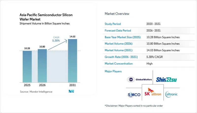
2025 年亞太地區半導體矽晶圓市場規模(以出貨量為準)為 102.8 億平方英寸,預計到 2031 年將從 2026 年的 108 億平方英寸成長至 140.3 億平方英寸,在預測期(2026-20331 年)年成長率為 5.38%。
中國、印度、日本和韓國「國產晶片」計畫的擴張正在推動新晶圓廠的建設,而超大規模資料中心和5G設備的需求也使得對300毫米優質拋光晶圓的需求持續旺盛。計劃在龍仁、平澤、台南、古吉拉突邦和北海道建設的大型產業叢集已確保了多年的晶圓供應,從而縮短了採購週期,並加劇了市場供應緊張。同時,高頻前端模組向SOI(絕緣薄膜矽)技術的轉變以及功率元件向碳化矽(SiC)和氮化鎵(GaN)技術的過渡正在改變產品結構,從而釋放出成熟的200毫米晶圓產能,用於模擬和離散半導體的生產。能源價格飆升帶來的價格壓力仍然是一個不利因素,但垂直整合和可再生能源相關合約正在減輕主要製造商的負擔。
亞太地區半導體矽晶圓市場趨勢及洞察。
5G智慧型手機的快速普及推動了對300毫米晶圓的需求。
5G終端出貨量的激增正推動前端模組和應用處理器向相容5nm或更小製程製程的300mm基板過渡。預計到2025年,中國當地的5G智慧型手機組裝貨量將超過2.8億部,而印度到同年年底將擁有1.8億5G用戶。因此,台南、華城和上海的晶圓廠的4nm和3nm製程節點幾乎運轉率運作。超低損耗基板對於毫米波設計至關重要,加速了高頻SOI(絕緣薄膜矽)技術的應用。高階智慧型手機升級週期的延長反而增加了單一手機的矽用量,即使銷售量趨於平穩,晶圓需求也得以穩定。
政府對國內半導體製造的補貼
目前,全部區域的資本投資計畫主要受財政獎勵主導。日本內閣已累計2兆日圓(約135億美元)用於在北海道建設一座2奈米晶圓代工廠;印度的「半導體使命」計畫已將其獎勵總額提高至150億美元;韓國已將資本投資的稅額扣抵提高至25%,刺激了龍仁市120兆韓元(約910億美元)的額外投資;中國第三期國家積體電路基金已註資3,440億元人民幣(約470億美元)用於擴大成熟製程節點。這些補貼將透過長期合約鞏固大規模批量晶圓訂單,即使新增產能,也會導致現貨市場供應減少和價格上漲。
超純多晶矽原料長期短缺
受能源發行政策的影響,預計到2025年底,新疆多晶矽產量將下降18%,現貨價格超過每公斤30美元,這將導致不自行採購原料的晶圓製造商的原料成本出現兩位數成長。德山和OCI正在利用流化床法增加2.5萬噸的產能,但商業化生產要到2027年或更晚才能開始。雖然信越化學和SUMCO等大型企業透過整合上游製程來維持利潤率,但規模較小的競爭對手卻被迫承受8至12週前置作業時間延長的負擔。
細分市場分析
2025年,300毫米晶圓將佔總出貨量的71.85%,這主要得益於邏輯裝置和高頻寬記憶體的微型化趨勢。在亞太半導體矽晶圓市場,隨著2奈米製程的基準柵(GaAA)電晶體增大晶片面積並提升單晶片晶圓需求,300毫米晶圓市場預計將比整體市場成長更快。該地區已有42家晶圓廠安裝了相關設備,僅信越化學位於白川的工廠預計到2025年外延晶圓月產量就將達到80萬片。
成熟的200mm晶圓生產線繼續為類比電源和感測器應用運作,這得益於向碳化矽轉型釋放出的產能。小於150mm的晶圓仍佔據不到5%的市場佔有率,主要用於砷化鎵和磷化銦裝置。 450mm先導計畫由於整體擁有成本(TCO)的挑戰而舉步維艱,缺陷密度仍高達損益平衡點的三倍。這一根深蒂固的問題凸顯了450mm技術商業性化之前必須克服的重大技術和經濟障礙。因此,這項延誤將推遲現有300mm供應鏈的轉型,而該供應鏈目前仍主導著半導體製造業。
預計到2025年,邏輯裝置將佔總出貨量的33.59%,主要得益於人工智慧、5G基頻和客製化加速器的發展。亞太地區半導體矽晶圓市場中邏輯元件的佔有率成長,得益於創紀錄的光刻掩模數量推高了單晶片的晶圓消耗量,而異構整合也進一步提升了基板的需求。記憶體緊隨其後,約佔30%,高頻寬記憶體的堆疊需要更厚的研磨製程和更薄的成品晶圓。
模擬和分立元件共同佔據了新釋放的200mm晶圓供應的大部分佔有率,為汽車動力傳動系統和工業自動化做出了貢獻。隨著雷射雷達(LiDAR)和飛行時間(ToF)技術的普及,感測器、微機電系統(MEMS)和光電子裝置(各自佔據中等個位數的市場佔有率)的總合需求持續成長。這些元件在汽車、消費性電子和工業等眾多應用領域中發揮著至關重要的作用,推動了其穩定成長。這種多元化策略有助於供應商應對智慧型手機銷售的周期性波動,並確保更穩定的收入來源。
《亞太半導體矽晶圓市場報告》依晶圓直徑(150毫米及以下、200毫米、300毫米)、半導體元件類型(邏輯元件、記憶體、類比元件、分立元件及其他)、晶圓類型(拋光面、外延面、絕緣體上矽(SOI)、單位及其他地區(SOI)市場預測以出貨量(平方英吋)為單位。
其他好處
- Excel格式的市場預測(ME)表
- 3個月的分析師支持
目錄
第1章:引言
- 研究假設和市場定義
- 調查範圍
第2章:調查方法
第3章執行摘要
第4章 市場狀況
- 市場概覽
- 市場促進因素
- 5G智慧型手機的快速普及推動了對300毫米晶圓的需求。
- 政府對國內半導體製造的補貼
- 快速部署人工智慧資料中心需要先進的邏輯節點
- 向碳化矽和氮化鎵過渡將釋放 200 毫米的生產能力。
- 通訊設備中對光子積體電路的需求激增
- 採用背面供電網路可提高 CMP 製程效率。
- 市場限制因素
- 超高純度多晶矽原料長期短缺
- 東亞能源價格上漲正在影響晶圓製造成本。
- 美國對先進製造設備的出口限制正在減緩產能擴張。
- 450mm試驗生產線的高缺陷率阻礙了投資。
- 產業價值鏈分析
- 技術分析
- 監理情勢
- 宏觀經濟因素的影響
- 波特五力分析
- 供應商的議價能力
- 買方的議價能力
- 新進入者的威脅
- 替代品的威脅
- 競爭公司之間的競爭
第5章 市場規模與成長預測
- 依晶圓直徑
- 150毫米或更小
- 200mm
- 300mm
- 依半導體裝置類型
- 邏輯
- 記憶
- 模擬
- 離散的
- 其他半導體裝置、光電子裝置、感測器、微型元件
- 依晶片類型
- 拋光
- 外延
- 絕緣體上矽(SOI)
- 特製矽,高電阻,高功率,感測器級。
- 最終用戶
- 家用電器
- 手機和智慧型手機
- PC 和伺服器
- 工業的
- 溝通
- 車
- 其他終端用戶應用程式
- 按地區
- 中國
- 日本
- 韓國
- 台灣
- 印度
- 亞太其他地區
第6章 競爭情勢
- 市場集中度
- 策略趨勢
- 市佔率分析
- 公司簡介
- Shin-Etsu Chemical Co., Ltd.
- SUMCO Corporation
- GlobalWafers Co., Ltd.
- SK Siltron Co., Ltd.
- Siltronic AG
- Wafer Works Corporation
- Okmetic Oy
- Soitec SA
- Ferrotec Holdings Corporation
- Hua Hong Semiconductor Ltd.
- ASML Holding NV
- LG Siltron CSS Inc.
- Poshing Technology Co., Ltd.
- Zhonghuan Semiconductor Co., Ltd.
- Mitsuboshi Diamond Industrial Co., Ltd.
- Hangzhou Silan Microelectronics Co., Ltd.
- Ningxia Xinri Hengli Silicon Materials Co., Ltd.
- Shanghai Simgui Technology Co., Ltd.
- Semiconductor Manufacturing International Corporation
- Formosa Sumco Technology Corporation
第7章 市場機會與未來展望
The Asia-Pacific Semiconductor Silicon Wafer Market size in terms of shipment volume was valued at 10.28 Billion Square Inches in 2025 and is estimated to grow from 10.80 Billion Square Inches in 2026 to reach 14.03 Billion Square Inches by 2031, at a CAGR of 5.38% during the forecast period (2026-2031).
Rising sovereign-chip programs across China, India, Japan, and South Korea are driving new fab construction, while hyperscale data centers and 5G devices keep demand for 300 mm prime-polished substrates elevated. Planned mega-clusters in Yongin, Pyeongtaek, Tainan, Gujarat, and Hokkaido have already secured multi-year wafer supply, shortening procurement cycles and tightening the merchant pool. Simultaneously, the shift toward silicon-on-insulator for radio-frequency front-end modules and the migration of power devices to silicon-carbide and gallium-nitride are reshaping the mix, freeing mature 200 mm capacity for analog and discretes. Price pressure from energy inflation remains a headwind, yet vertical integration and renewable-energy contracts are cushioning leading producers.
Asia-Pacific Semiconductor Silicon Wafer Market Trends and Insights
Soaring 5G Smartphone Penetration Boosting 300 mm Wafer Demand
A steep rise in 5G handset shipments is shifting front-end modules and application processors onto 300 mm substrates that support sub-5 nm lithography. Mainland assemblers shipped more than 280 million 5G smartphones in 2025, and India ended the same year with 180 million 5G subscribers. Foundries in Tainan, Hwaseong, and Shanghai are therefore operating at near full utilization for 4 nm and 3 nm nodes. Radio-frequency silicon-on-insulator uptake has accelerated as millimeter-wave designs mandate ultra-low loss substrates. Longer upgrade cycles for premium phones paradoxically lift total silicon content per unit, stabilizing wafer pull even when unit sales plateau.
Government Subsidies for Domestic Semiconductor Manufacturing
Fiscal incentives now dominate capital-expenditure roadmaps across the region. The Japanese cabinet earmarked JPY 2 trillion (USD 13.5 billion) for a 2 nm foundry in Hokkaido, and India's Semiconductor Mission raised its incentive pool to USD 15 billion. South Korea raised tax credits to 25% of cap-ex, encouraging an additional KRW 120 trillion (USD 91 billion) commitment in Yongin. China's third National IC Fund injected CNY 344 billion (USD 47 billion) into mature-node expansions. These subsidies lock in large wafer call-offs under long-term contracts, thereby shrinking spot-market availability and nudging prices upward despite new capacity.
Chronic Shortages of Ultrapure Polysilicon Feedstock
Polysilicon production in Xinjiang fell 18% in late 2025 following energy-rationing directives, pushing spot prices above USD 30 per kg and inflating raw-material costs by double digits for wafer producers without captive feedstock. While Tokuyama and OCI are adding 25,000 metric tons of new fluidized-bed capacity, commercial output will not arrive before 2027. Larger players such as Shin-Etsu Chemical and SUMCO protect margins through upstream integration, leaving smaller rivals saddled with 8-to-12-week lead-time extensions.
Other drivers and restraints analyzed in the detailed report include:
- Rapid Deployment of AI Data Centers Requiring Advanced Logic Nodes
- Silicon-Carbide and GaN Transition Freeing 200 mm Capacity
- Escalating Energy Prices in East Asia Impacting Wafer-Fab Costs
For complete list of drivers and restraints, kindly check the Table Of Contents.
Segment Analysis
The 300 mm class accounted for 71.85% of total shipments in 2025, driven by logic and high-bandwidth memory scaling. Asia-Pacific semiconductor silicon wafer market size for 300 mm substrates is expected to expand faster than the overall baseline as gate-all-around transistors at 2 nm inflate die area and drive per-chip wafer pull. Installed base already spans 42 fabs across the region, and Shin-Etsu's Shirakawa plant alone lifted epitaxial output to 800,000 wafers per month in 2025.
Mature 200 mm lines continue to serve analog power and sensor applications, buffered by capacity freed up by silicon-carbide migration. Wafers up to 150 mm remain a sub-5% niche for gallium arsenide and indium phosphide devices. Cost-of-ownership challenges leave 450 mm pilots in a quandary, as defect densities remain thrice the threshold for break-even yields. This persistent issue highlights the significant technical and economic barriers that need to be addressed before 450 mm technology can achieve commercial viability. Consequently, this setback postpones any shake-up to the established 300 mm supply chain, which continues to dominate the semiconductor manufacturing landscape.
Logic devices accounted for 33.59% of shipments in 2025, lifted by AI, 5G basebands, and custom accelerators. Asia-Pacific semiconductor silicon wafer market share for logic is supported by record reticle counts that raise wafer consumption per chip, while heterogeneous integration adds to substrate demand. Memory followed at roughly 30%, with high-bandwidth-memory stacks driving thicker grind steps and thinner finished wafers.
Analog and discrete together absorb most of the newly liberated 200 mm supply, serving automotive powertrains and industrial automation. As lidar and time-of-flight technologies gain traction, the combined wafer pull for sensors, MEMS, and optoelectronics-each holding a high single-digit share-continues to rise. These components play a critical role in various applications, including automotive, consumer electronics, and industrial sectors, driving their steady growth. This diversification strategy helps suppliers weather the cyclical fluctuations of smartphone sales, ensuring a more stable revenue stream.
The Asia-Pacific Semiconductor Silicon Wafer Market Report is Segmented by Wafer Diameter (Up To 150 Mm, 200 Mm, 300 Mm), Semiconductor Device Type (Logic, Memory, Analog, Discrete, and More), Wafer Type (Prime Polished, Epitaxial, Silicon-On-Insulator (SOI), Specialty Silicon), End-User (PCs and Servers, Industrial, Automotive, and More), and Geography. The Market Forecasts are Provided in Terms of Shipment Volume (Square Inches).
List of Companies Covered in this Report:
- Shin-Etsu Chemical Co., Ltd.
- SUMCO Corporation
- GlobalWafers Co., Ltd.
- SK Siltron Co., Ltd.
- Siltronic AG
- Wafer Works Corporation
- Okmetic Oy
- Soitec SA
- Ferrotec Holdings Corporation
- Hua Hong Semiconductor Ltd.
- ASML Holding N.V.
- LG Siltron CSS Inc.
- Poshing Technology Co., Ltd.
- Zhonghuan Semiconductor Co., Ltd.
- Mitsuboshi Diamond Industrial Co., Ltd.
- Hangzhou Silan Microelectronics Co., Ltd.
- Ningxia Xinri Hengli Silicon Materials Co., Ltd.
- Shanghai Simgui Technology Co., Ltd.
- Semiconductor Manufacturing International Corporation
- Formosa Sumco Technology Corporation
Additional Benefits:
- The market estimate (ME) sheet in Excel format
- 3 months of analyst support
TABLE OF CONTENTS
1 INTRODUCTION
- 1.1 Study Assumptions and Market Definition
- 1.2 Scope of the Study
2 RESEARCH METHODOLOGY
3 EXECUTIVE SUMMARY
4 MARKET LANDSCAPE
- 4.1 Market Overview
- 4.2 Market Drivers
- 4.2.1 Soaring 5G Smartphone Penetration Boosting 300 mm Wafer Demand
- 4.2.2 Government Subsidies for Domestic Semiconductor Manufacturing
- 4.2.3 Rapid Deployment of AI Data Centers Requiring Advanced Logic Nodes
- 4.2.4 Silicon Carbide and GaN Transition Freeing 200 mm Capacity
- 4.2.5 Surging Demand for Photonic Integrated Circuits in Telecom Gear
- 4.2.6 Adoption of Backside Power Delivery Networks Increasing CMP Steps
- 4.3 Market Restraints
- 4.3.1 Chronic Shortages of Ultrapure Polysilicon Feedstock
- 4.3.2 Escalating Energy Prices in East Asia Impacting Wafer Fab Costs
- 4.3.3 US Export Controls on Advanced Tools Delaying Capacity Expansions
- 4.3.4 High Defect Density in 450 mm Pilot Lines Hindering Investments
- 4.4 Industry Value-Chain Analysis
- 4.5 Technology Analysis
- 4.6 Regulatory Landscape
- 4.7 Impact of Macroeconomic Factors
- 4.8 Porter's Five Forces Analysis
- 4.8.1 Bargaining Power of Suppliers
- 4.8.2 Bargaining Power of Buyers
- 4.8.3 Threat of New Entrants
- 4.8.4 Threat of Substitutes
- 4.8.5 Intensity of Competitive Rivalry
5 MARKET SIZE AND GROWTH FORECASTS (VOLUME)
- 5.1 By Wafer Diameter
- 5.1.1 Up to 150 mm
- 5.1.2 200 mm
- 5.1.3 300 mm
- 5.2 By Semiconductor Device Type
- 5.2.1 Logic
- 5.2.2 Memory
- 5.2.3 Analog
- 5.2.4 Discrete
- 5.2.5 Other Semiconductor Device Types, Optoelectronics, Sensors, Micro
- 5.3 By Wafer Type
- 5.3.1 Prime Polished
- 5.3.2 Epitaxial
- 5.3.3 Silicon-on-Insulator, SOI
- 5.3.4 Specialty Silicon, High-Resistivity, Power, Sensor-Grade
- 5.4 By End-user
- 5.4.1 Consumer Electronics
- 5.4.2 Mobile and Smartphones
- 5.4.3 PCs and Servers
- 5.4.4 Industrial
- 5.4.5 Telecommunications
- 5.4.6 Automotive
- 5.4.7 Other End-user Applications
- 5.5 By Geography
- 5.5.1 China
- 5.5.2 Japan
- 5.5.3 South Korea
- 5.5.4 Taiwan
- 5.5.5 India
- 5.5.6 Rest of Asia-Pacific
6 COMPETITIVE LANDSCAPE
- 6.1 Market Concentration
- 6.2 Strategic Moves
- 6.3 Market Share Analysis
- 6.4 Company Profiles (includes Global Level Overview, Market Level Overview, Core Segments, Financials as available, Strategic Information, Market Rank/Share, Products and Services, Recent Developments)
- 6.4.1 Shin-Etsu Chemical Co., Ltd.
- 6.4.2 SUMCO Corporation
- 6.4.3 GlobalWafers Co., Ltd.
- 6.4.4 SK Siltron Co., Ltd.
- 6.4.5 Siltronic AG
- 6.4.6 Wafer Works Corporation
- 6.4.7 Okmetic Oy
- 6.4.8 Soitec SA
- 6.4.9 Ferrotec Holdings Corporation
- 6.4.10 Hua Hong Semiconductor Ltd.
- 6.4.11 ASML Holding N.V.
- 6.4.12 LG Siltron CSS Inc.
- 6.4.13 Poshing Technology Co., Ltd.
- 6.4.14 Zhonghuan Semiconductor Co., Ltd.
- 6.4.15 Mitsuboshi Diamond Industrial Co., Ltd.
- 6.4.16 Hangzhou Silan Microelectronics Co., Ltd.
- 6.4.17 Ningxia Xinri Hengli Silicon Materials Co., Ltd.
- 6.4.18 Shanghai Simgui Technology Co., Ltd.
- 6.4.19 Semiconductor Manufacturing International Corporation
- 6.4.20 Formosa Sumco Technology Corporation
7 MARKET OPPORTUNITIES AND FUTURE OUTLOOK
- 7.1 White-Space and Unmet-Need Assessment
 矽晶圓市場-全球產業規模、佔有率、趨勢、機會和預測:按晶圓尺寸、類型、應用、最終用戶、地區和競爭格局分類,2021-2031年
 矽晶圓市場規模、佔有率、趨勢和預測:按晶圓尺寸、類型、應用、最終用途和地區分類,2026-2034 年
 半導體矽晶圓回收市場:依回收製程、晶圓類型、晶圓尺寸、應用領域、產業及最終用戶分類-2026-2032年全球市場預測
 2026-2034年全球太陽能矽晶圓市場規模、佔有率、趨勢和成長分析報告
 5G半導體矽晶圓:市場佔有率分析、產業趨勢與統計及成長預測(2026-2031年)工業半導體矽晶圓:市場佔有率分析、產業趨勢與統計、成長預測(2026-2031)用於功率元件的矽晶圓:市場佔有率分析、行業趨勢和統計數據以及成長預測(2026-2031 年)高阻矽晶圓:市佔率分析、產業趨勢與統計、成長預測(2026-2031 年)
 2026 年至 2035 年太陽能電池用矽晶圓市場的機會、成長要素、產業趨勢分析與預測。中國半導體矽晶圓市場:市場佔有率分析、產業趨勢與統計及成長預測(2026-2031年)