

 |
市場調查報告書
商品編碼
2043999
日本半導體矽晶圓市場:市場佔有率分析、產業趨勢與統計、成長預測(2026-2031)Japan Semiconductor Silicon Wafer - Market Share Analysis, Industry Trends & Statistics, Growth Forecasts (2026 - 2031) |
||||||
※ 本網頁內容可能與最新版本有所差異。詳細情況請與我們聯繫。
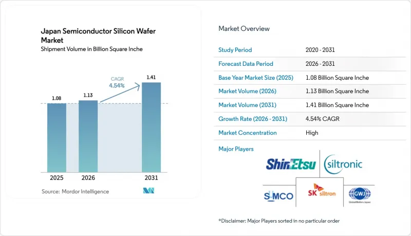
日本半導體矽晶圓市場規模(以出貨量為準)預計將從 2025 年的 10.8 億平方英寸,2026 年的 11.3 億平方英寸,到 2031 年達到 14.1 億平方英寸,2026 年至 2031 年的複合年成長率為 4.54%。
政策制定者將上游材料置於推動製造業回流的核心位置,將多年補貼與本地晶圓生產、先進封裝以及2奈米邏輯晶片的研發準備掛鉤。隨著新型邏輯晶片和高頻寬記憶體生產線的擴張,市場對300毫米基板的需求日益集中,同時,汽車和射頻(RF)設計領域對特種矽的需求也不斷成長。儘管大型成熟企業仍能維持規模經濟,但不斷上漲的電力成本和嚴格的廢水排放法規正在擠壓利潤空間,為靈活的特殊晶圓供應商創造了利基市場。勞動力短缺和智慧型手機市場的周期性波動仍然是短期內的主要限制因素,但長期的汽車行業合約以及國內大型晶圓廠的擴張正在支撐日本半導體矽晶圓市場的中期成長前景。
日本半導體矽晶圓市場趨勢與洞察
邏輯儲存裝置對 300mm 晶圓的需求增加。
2025年,受人工智慧(AI)加速器和16奈米以下邏輯半導體產量成長的推動,300毫米基板的出貨量年增5.8%。熊本工廠第一期生產線每月消耗約5.5萬片晶圓,而到2027年底的二期擴建工程將新增5萬片晶圓的產能,使國內需求每年增加超過120萬片。 DRAM和NAND快閃記憶體並行製程小型化正在削弱200毫米設備的成本優勢,加速朝向更大直徑晶圓的轉變。晶體生長設備的前置作業時間仍然約為18個月,導致供應延遲和市場持續緊張。因此,這些因素構成了支撐日本半導體矽晶圓市場中期成長的基礎。
政府補貼以擴大國內晶圓生產能力
在2026會計年度預算中,日本經濟產業省累計1.23兆日圓(約87億美元)用於半導體基礎建設,其中4,000億日圓(約28億美元)用於晶圓生產線、外延設備和材料的研發。相關融資協議要求供應商達到國內就業和技術轉移目標,從而確保短期內新增300台300毫米拉絲機和外延反應器。信越化學和SUMCO兩家公司共獲得950億日元(約6.7億美元)的資金,用於在2027年前將產能提高15%,而中型企業則獲得了用於特種矽的小規模津貼。由於此類領先投資的性質,預計日本半導體矽晶圓市場將立即迎來供應成長,從而抵消因遵守環境法規而產生的資本密集度。
全球智慧型手機需求長期低迷
2025年初連續三個季度出貨量下滑,導致高利潤邏輯晶圓對海外代工廠的出口減少。信越化學關閉了兩座拉片生產線,並推遲了一項300億日元(約2.1億美元)的擴建計劃,而SUMCO則將銷售預期下調了7%。訂單損失將對盈利產生重大影響,因為智慧型手機處理器和NAND快閃記憶體控制器對晶圓的平整度和污染程度要求極高。復甦取決於5G在價格敏感型市場的普及程度,這將導致日本半導體矽晶圓市場在可預見的未來產運轉率出現缺口。
細分市場分析
預計到2025年,300mm晶圓將佔日本半導體矽晶圓市場的71.28%,繼續以4.95%的複合年成長率成長,超過小尺寸晶圓。隨著製程節點向16奈米以下邁進以及高頻寬記憶體堆疊技術的應用,大面積基板對於成本攤銷至關重要。預計到2028年,熊本和北海道兩家晶圓廠的年需求量將超過200萬片晶圓。由於供應緊張,晶圓廠正在投資建造新的直拉式製程設備和先進的拋光生產線,但由於設備前置作業時間長達18個月,預計供應狀況的改善要到2027年中期才能實現。
同時,200mm晶圓在類比、功率和微控制器的生產中仍扮演著重要角色,在這些應用中,成熟的製程配方比晶片密度更為重要。儘管由於汽車電氣化、工業自動化和感測器需求的成長,設備供應商減少了備件支持,但200mm晶圓廠的產能仍然接近運作。直徑達150mm的晶圓仍是一個小眾市場,約佔總產量的5%,主要用於原型製作和特殊射頻裝置,在這些應用中,快速的週期比規模經濟更為重要。這種複雜的市場前景表明,300mm基板在日本半導體矽晶圓市場的佔有率將繼續逐步成長,而小直徑晶圓的產量預計將保持穩定,不會出現下滑。
預計到2025年,邏輯裝置將佔日本半導體矽晶圓市場佔有率的36.29%,隨著3奈米製程實現國產化,其複合年成長率將達到5.05%。 2027年起,Rapidus將在北海道引進2奈米製程產能,實現多元化經營,進一步推動日本北部地區的晶圓需求。記憶體市場將緊隨其後,複合年成長率將達到4.6%,這主要得益於整合高頻寬DRAM堆疊和用於邊緣儲存的高密度NAND快閃記憶體的人工智慧(AI)伺服器。
在長達數年的工業和通訊設計週期中,模擬裝置的需求持續成長,而分立元件則正轉向碳化矽 (SiC) 和氮化鎵 (GaN) 等材料,用於高壓汽車逆變器。隨著雷射雷達 (LiDAR) 和飛行時間 (ToF) 技術在高級駕駛輔助系統 (ADAS) 中的應用日益廣泛,感測器和光電子等專業領域也正加速成長。這種均衡的市場組成凸顯了保護日本半導體矽晶圓市場免受單一領域衝擊以及維持整個裝置系列廣泛產品線的戰略價值。
《日本半導體矽晶圓市場報告》按晶圓直徑(150毫米及以下、200毫米、300毫米)、半導體裝置類型(邏輯裝置、記憶體、模擬器等)、晶圓類型(拋光面、外延面、絕緣體上矽(SOI)等)、最終用戶(家用電子電器市場/區域進行/地區進行細分(消費設備/國家/地區電腦/地區電腦)。市場預測以體積(平方英吋)為單位。
其他好處:
- Excel格式的市場預測(ME)表
- 3個月的分析師支持
目錄
第1章:引言
- 研究假設和市場定義
- 調查範圍
第2章:調查方法
第3章執行摘要
第4章 市場狀況
- 市場概覽
- 產業價值鏈分析
- 技術分析
- 監理情勢
- 宏觀經濟因素的影響
- 市場促進因素
- 邏輯元件和記憶體對 300mm 晶圓的需求增加。
- 政府補貼以擴大國內晶圓生產能力
- 台積電和SONY合資興建熊本巨型工廠
- 加速日本汽車產業的電氣化進程
- IDM公司將供應鏈遷回日本(回流)的舉措
- Float-Zone-切克勞斯基混合晶體拉絲技術的突破性進展
- 市場限制因素
- 全球智慧型手機需求長期低迷
- 高昂的電力成本影響製造業競爭力
- 矽加工中嚴格的廢水處理法規
- 晶體生長操作技術人員短缺
- 波特五力分析
- 供應商的議價能力
- 買方的議價能力
- 新進入者的威脅
- 替代品的威脅
- 競爭公司之間的競爭
第5章 市場規模與成長預測
- 依晶圓直徑
- 最大可達 150 毫米
- 200 mm
- 300 mm
- 以半導體裝置類型分類
- 邏輯
- 記憶
- 模擬
- 離散的
- 其他類型的半導體裝置(光電子元件、感測器、微型元件)
- 依晶片類型
- 拋光
- 外延
- 絕緣體上矽(SOI)
- 特種矽(高電阻、高功率、感測器級)
- 最終用戶
- 家用電子電器
- 行動裝置和智慧型手機
- 個人電腦和伺服器
- 工業的
- 溝通
- 車
- 其他最終用戶
第6章 競爭情勢
- 市場集中度
- 策略趨勢
- 市佔率分析
- 公司簡介
- Shin-Etsu Chemical Co., Ltd.
- SUMCO Corporation
- GlobalWafers Japan Co., Ltd.
- Siltronic AG
- SK Siltron Co., Ltd.
- Okmetic Oy
- Wafer Works Corporation
- Ferrotec Holdings Corporation
- Mitsubishi Materials Corporation
- Tokuyama Corporation
- Resonac Holdings Corporation
- National Silicon Industry Group(NSIG)
- Hebei Zhonghuan Semiconductor Co., Ltd.
- Topsil GlobalWafers A/S
- Soitec SA
- SEH America, Inc.
- MEMC Electronic Materials, Inc.
- Elkem ASA
- Shanghai Advanced Silicon Technology Co., Ltd.
- Siltronic Japan Corp.
第7章 市場機會與未來展望
The Japan Semiconductor Silicon Wafer Market size in terms of shipment volume is expected to increase from 1.08 Billion Square Inche in 2025 to 1.13 Billion Square Inche in 2026 and reach 1.41 Billion Square Inche by 2031, growing at a CAGR of 4.54% over 2026-2031.
Policy makers have placed upstream materials at the center of the country's re-shoring push, tying multi-year subsidies to local wafer output, advanced packaging, and 2-nanometer logic readiness. Demand is clustering around 300 millimeter substrates as new logic and high-bandwidth memory lines ramp, while specialty silicon gains traction in automotive and radio-frequency designs. Large incumbents maintain scale advantages, yet rising power tariffs and strict wastewater rules compress margins and open niches for agile specialty-wafer suppliers. Talent shortages and smartphone cyclicality remain the main near-term brakes, but long-duration automotive contracts and domestic mega-fab expansions underpin the medium-term growth outlook for the Japan semiconductor silicon wafer market.
Japan Semiconductor Silicon Wafer Market Trends and Insights
Rising Demand For 300 mm Wafers In Logic And Memory Devices
Shipments of 300-millimeter substrates grew 5.8% year on year in 2025 as artificial-intelligence accelerators and sub-16-nanometer logic scaled up volume. The first Kumamoto line alone pulls roughly 55,000 wafers each month, and its phase-two expansion adds another 50,000 by late 2027, lifting domestic demand by more than 1.2 million wafers annually. Parallel node migrations in DRAM and NAND eliminate the cost advantage of 200 millimeter tools, intensifying the swing toward larger diameters. Crystal-growth equipment lead times hover at 18 months, delaying supply responses and preserving tight market conditions. This driver, therefore, anchors mid-term growth for the Japan semiconductor silicon wafer market.
Government Subsidies For Domestic Wafer Capacity Expansion
The Ministry of Economy, Trade and Industry budgeted JPY 1.23 trillion (USD 8.7 billion) for semiconductor infrastructure in fiscal 2026, with JPY 400 billion (USD 2.8 billion) ring-fenced for wafer lines, epitaxial tools, and materials R and D. Funding agreements oblige suppliers to hit domestic employment and technology-transfer targets, ensuring near-term installation of an additional 300 millimeter pullers and epitaxial reactors. Shin-Etsu and SUMCO together secured JPY 95 billion (USD 670 million) to lift capacity by 15% through 2027, while midsize firms accessed smaller grants for specialty silicon. The front-loaded nature of disbursements gives the Japan semiconductor silicon wafer market an immediate volume boost and offsets the capital intensity of environmental compliance.
Prolonged Downturn In Global Smartphone Demand
Three consecutive quarters of shipment contraction in early 2025 cut high-margin logic-wafer exports to overseas foundries. Shin-Etsu idled two pullers and deferred a JPY 30 billion (USD 210 million) expansion, while SUMCO trimmed revenue guidance by 7% . Because smartphone processors and NAND controllers require tight flatness and low contamination, the lost orders carry outsized profitability. Recovery hinges on 5 G penetration in price-sensitive markets, leaving a near-term hole in utilization rates for the Japan semiconductor silicon wafer market.
Other drivers and restraints analyzed in the detailed report include:
- Kumamoto Mega-Fab Build-out By TSMC-Sony JV
- Accelerated Electrification Of Japanese Automotive Industry
- High Electricity Costs Affecting Manufacturing Competitiveness
For complete list of drivers and restraints, kindly check the Table Of Contents.
Segment Analysis
The 300 millimeter category dominated the Japan semiconductor silicon wafer market size with a 71.28% volume share in 2025 and continues to outgrow smaller diameters at a 4.95% CAGR. Node migrations below 16 nanometers and high-bandwidth memory stacking make large-area substrates essential for cost amortization, and the Kumamoto and Hokkaido fabs together will require more than 2 million wafers annually by 2028. Tight supply directs capital toward new Czochralski pullers and advanced polishing lines, yet 18-month tool lead times delay relief until mid-2027.
Conversely, the 200 millimeter segment retains an entrenched role in analog, power and microcontroller production that favors proven process recipes over die density. Automotive electrification, industrial automation and sensor demand keep 200 millimeter fabs running near full utilization, even as equipment suppliers wind down spare-parts support. Diameters up to 150 millimeters remain niche at roughly 5% of volume, serving prototyping and specialty RF devices where quick cycle times trump economies of scale. This mixed outlook means the Japan semiconductor silicon wafer market share for 300 millimeter substrates will keep inching upward, while volumes for smaller diameters hold steady rather than fall.
Logic devices captured 36.29% of Japan's semiconductor silicon wafer market share in 2025, with expansion set at a 5.05% CAGR as 3-nanometer production localizes. Rapidus adds diversification by introducing 2-nanometer capacity in Hokkaido after 2027, anchoring additional wafer pull in northern Japan. Memory follows at 4.6% CAGR, buoyed by artificial-intelligence servers that integrate high-bandwidth DRAM stacks and dense NAND for edge storage.
Analog demand grows steadily across multi-year industrial and telecom design cycles, whereas discrete devices pivot toward silicon carbide and gallium nitride for high-voltage automotive inverters. Specialty categories such as sensors and optoelectronics accelerate alongside lidar and time-of-flight adoption in advanced driver-assistance systems. This balanced mix cushions the Japan semiconductor silicon wafer market against single-segment shocks and underscores the strategic value of maintaining breadth across device families.
The Japan Semiconductor Silicon Wafer Market Report is Segmented by Wafer Diameter (Up To 150 Mm, 200 Mm, and 300 Mm), Semiconductor Device Type (Logic, Memory, Analog, and More), Wafer Type (Prime Polished, Epitaxial, Silicon-On-Insulator (SOI), and More), End-User (Consumer Electronics, Mobile and Smartphones, Pcs and Servers, and More), and Country. The Market Forecasts are Provided in Terms of Volume (Square Inches).
List of Companies Covered in this Report:
- Shin-Etsu Chemical Co., Ltd.
- SUMCO Corporation
- GlobalWafers Japan Co., Ltd.
- Siltronic AG
- SK Siltron Co., Ltd.
- Okmetic Oy
- Wafer Works Corporation
- Ferrotec Holdings Corporation
- Mitsubishi Materials Corporation
- Tokuyama Corporation
- Resonac Holdings Corporation
- National Silicon Industry Group (NSIG)
- Hebei Zhonghuan Semiconductor Co., Ltd.
- Topsil GlobalWafers A/S
- Soitec SA
- SEH America, Inc.
- MEMC Electronic Materials, Inc.
- Elkem ASA
- Shanghai Advanced Silicon Technology Co., Ltd.
- Siltronic Japan Corp.
Additional Benefits:
- The market estimate (ME) sheet in Excel format
- 3 months of analyst support
TABLE OF CONTENTS
1 INTRODUCTION
- 1.1 Study Assumptions and Market Definition
- 1.2 Scope of the Study
2 RESEARCH METHODOLOGY
3 EXECUTIVE SUMMARY
4 MARKET LANDSCAPE
- 4.1 Market Overview
- 4.2 Industry Value-Chain Analysis
- 4.3 Technology Analysis
- 4.4 Regulatory Landscape
- 4.5 Impact of Macroeconomic Factors
- 4.6 Market Drivers
- 4.6.1 Rising Demand for 300 mm Wafers in Logic and Memory Devices
- 4.6.2 Government Subsidies for Domestic Wafer Capacity Expansion
- 4.6.3 Kumamoto Mega-Fab Build-out by TSMC-Sony JV
- 4.6.4 Accelerated Electrification of Japanese Automotive Industry
- 4.6.5 Supply-Chain Re-Shoring Initiatives among IDMs
- 4.6.6 Breakthrough in Float-Zone-Czochralski Hybrid Crystal Pulling
- 4.7 Market Restraints
- 4.7.1 Prolonged Downturn in Global Smartphone Demand
- 4.7.2 High Electricity Costs Affecting Manufacturing Competitiveness
- 4.7.3 Stringent Waste-Water Regulations on Silicon Processing
- 4.7.4 Engineering Talent Shortage in Crystal Growth Operations
- 4.8 Porter's Five Forces Analysis
- 4.8.1 Bargaining Power of Suppliers
- 4.8.2 Bargaining Power of Buyers
- 4.8.3 Threat of New Entrants
- 4.8.4 Threat of Substitutes
- 4.8.5 Intensity of Competitive Rivalry
5 MARKET SIZE AND GROWTH FORECASTS (VOLUME)
- 5.1 By Wafer Diameter
- 5.1.1 Up to 150 mm
- 5.1.2 200 mm
- 5.1.3 300 mm
- 5.2 By Semiconductor Device Type
- 5.2.1 Logic
- 5.2.2 Memory
- 5.2.3 Analog
- 5.2.4 Discrete
- 5.2.5 Other Semiconductor Device Types (Optoelectronics, Sensors, Micro)
- 5.3 By Wafer Type
- 5.3.1 Prime Polished
- 5.3.2 Epitaxial
- 5.3.3 Silicon-on-Insulator (SOI)
- 5.3.4 Specialty Silicon (High-Resistivity, Power, Sensor-Grade)
- 5.4 By End-User
- 5.4.1 Consumer Electronics
- 5.4.2 Mobile and Smartphones
- 5.4.3 PCs and Servers
- 5.4.4 Industrial
- 5.4.5 Telecommunications
- 5.4.6 Automotive
- 5.4.7 Other End-User
6 COMPETITIVE LANDSCAPE
- 6.1 Market Concentration
- 6.2 Strategic Moves
- 6.3 Market Share Analysis
- 6.4 Company Profiles (includes Global Level Overview, Market Level Overview, Core Segments, Financials as available, Strategic Information, Market Rank/Share, Products and Services, Recent Developments)
- 6.4.1 Shin-Etsu Chemical Co., Ltd.
- 6.4.2 SUMCO Corporation
- 6.4.3 GlobalWafers Japan Co., Ltd.
- 6.4.4 Siltronic AG
- 6.4.5 SK Siltron Co., Ltd.
- 6.4.6 Okmetic Oy
- 6.4.7 Wafer Works Corporation
- 6.4.8 Ferrotec Holdings Corporation
- 6.4.9 Mitsubishi Materials Corporation
- 6.4.10 Tokuyama Corporation
- 6.4.11 Resonac Holdings Corporation
- 6.4.12 National Silicon Industry Group (NSIG)
- 6.4.13 Hebei Zhonghuan Semiconductor Co., Ltd.
- 6.4.14 Topsil GlobalWafers A/S
- 6.4.15 Soitec SA
- 6.4.16 SEH America, Inc.
- 6.4.17 MEMC Electronic Materials, Inc.
- 6.4.18 Elkem ASA
- 6.4.19 Shanghai Advanced Silicon Technology Co., Ltd.
- 6.4.20 Siltronic Japan Corp.
7 MARKET OPPORTUNITIES AND FUTURE OUTLOOK
- 7.1 White-Space and Unmet-Need Assessment
 矽晶圓市場-全球產業規模、佔有率、趨勢、機會和預測:按晶圓尺寸、類型、應用、最終用戶、地區和競爭格局分類,2021-2031年
 矽晶圓市場規模、佔有率、趨勢和預測:按晶圓尺寸、類型、應用、最終用途和地區分類,2026-2034 年
 半導體矽晶圓回收市場:依回收製程、晶圓類型、晶圓尺寸、應用領域、產業及最終用戶分類-2026-2032年全球市場預測
 2026-2034年全球太陽能矽晶圓市場規模、佔有率、趨勢和成長分析報告
 5G半導體矽晶圓:市場佔有率分析、產業趨勢與統計及成長預測(2026-2031年)工業半導體矽晶圓:市場佔有率分析、產業趨勢與統計、成長預測(2026-2031)用於功率元件的矽晶圓:市場佔有率分析、行業趨勢和統計數據以及成長預測(2026-2031 年)高阻矽晶圓:市佔率分析、產業趨勢與統計、成長預測(2026-2031 年)
 2026 年至 2035 年太陽能電池用矽晶圓市場的機會、成長要素、產業趨勢分析與預測。中國半導體矽晶圓市場:市場佔有率分析、產業趨勢與統計及成長預測(2026-2031年)