


 |
市場調查報告書
商品編碼
2043996
德國半導體矽晶圓:市場佔有率分析、產業趨勢與統計及成長預測(2026-2031)Germany Semiconductor Silicon Wafer - Market Share Analysis, Industry Trends & Statistics, Growth Forecasts (2026 - 2031) |
||||||
※ 本網頁內容可能與最新版本有所差異。詳細情況請與我們聯繫。
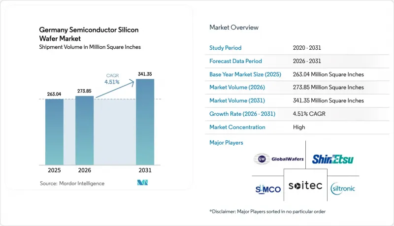
2025 年德國半導體矽晶圓市場(以出貨量為準)價值 2.6304 億平方英寸,預計到 2031 年將從 2026 年的 2.7385 億平方英寸成長至 3.4135 億平方英寸,預測期內複合年成長率為 4.51%。
(2026-2031)。
以英特爾、台積電、英飛凌和全球晶圓代工廠為核心的300毫米邏輯和功率裝置晶圓廠的多年擴張,正在推動對優質拋光和外延基板的長期需求,與此同時,合約價格也在收緊。企業購買風能和太陽能的電力協議正在縮小德國與亞洲之間歷史上存在的能源成本差距,加劇了德國半導體矽晶圓市場的競爭。同時,量子技術向Float-Zone高純度晶圓的轉變以及汽車雷達向全耗盡SOI晶圓的轉變,正在推動特種晶圓領域的成長。然而,多晶矽價格的波動和持續高企的工業關稅繼續擠壓短期利潤空間,迫使生產商優先考慮高價值領域和長期採購協議。
德國半導體晶圓市場趨勢與洞察
一項穩健的資本投資計劃,用於擴建德國的 300 毫米晶圓廠。
英特爾於2025年中期在馬格德堡啟動了兩座晶圓廠的建設,這是其300億歐元(340億美元)投資計畫的一部分,旨在2028年投產時提供5奈米以下邏輯晶片的生產能力。台積電、博世、英飛凌和恩智浦在德勒斯登共同成立了「歐洲半導體製造公司」。這是一個投資100億歐元(113億美元)的項目,計劃到2027年採用28奈米、22奈米和16奈米工藝,每月生產4萬片晶圓。英飛凌投資50億歐元(57億美元)的「智慧功率晶圓廠」於2025年初開始試生產,旨在一條300毫米生產線上生產碳化矽和高壓矽。全球晶圓代工廠正在通過一項耗資 11 億歐元(12.5 億美元)的擴建計劃,將其位於德累斯頓工廠的 300 毫米晶圓年產能提高 100 千萬片,該計劃將於 2028 年完成。這些項目將共同縮短拋光晶圓的前置作業時間,並確保簽訂多年期的收購契約,從而支持市場的長期成長軌跡。
預計從2025年起汽車晶片需求將復甦
德國汽車產量預計在2024年恢復至410萬輛,晶片訂單在2022-2023年庫存調整期間停滯不前,目前也已復甦。英飛凌報告稱,2025年電動車(EV)動力系統功率元件的出貨量將實現兩位數成長,其中碳化矽(SiC)MOSFET在保時捷Taycan等量產車型中的效率比矽IGBT提高了3%。需求成長的驅動力是向800V電池系統的轉變,這需要摻雜偏差小於2%的高壓外延晶圓。將於2025年生效的歐盟7排放標準將強制每輛車配備多個感測器和微控制器,這將進一步增加所需的晶圓數量。隨著汽車製造商確保供應,晶圓經銷商因長期合約和嚴格的規格要求而受益於溢價。
多晶矽價格波動劇烈
由於中國供應商年產能增加40萬噸,半導體多晶矽價格從2022年初的每公斤35美元暴跌至2024年12月的每公斤6.50美元。 Siltronic公司表示,2025年上半年原物料成本下降了12%,但警告稱,現貨價格仍比長期合約的下限低40%,這給投資計畫帶來了不確定性。如果價格迅速回升至每公斤20美元,除非裝置製造商接受價格上漲,否則晶圓製造商的利潤率將下降3-5個百分點。這種不確定性使得小型製造商不願投資新的柴可拉斯基法晶圓機設備,導致垂直整合的競爭對手透過提煉自身原料來進一步鞏固市場佔有率。在價格穩定之前,預計供應商在增產方面仍將保持謹慎。
細分市場分析
到2025年,德國半導體矽晶圓市場中,300毫米晶圓將佔74.68%的出貨量,遙遙領先其他所有尺寸。用於製造尖端邏輯裝置和汽車功率裝置的標準化設備均圍繞此尺寸規格展開,其有效晶片面積為200毫米晶圓的兩倍以上,單晶片加工成本降低約30%。英特爾位於馬格德堡的工廠對晶圓表面平整度要求不超過0.08微米,總厚度偏差不超過0.15微米,因此只有信越化學和SUMCO等公司的優質供應商才能獲得認證。
2025年,晶體提取的前置作業時間延長至24個月,導致300毫米優質拋光晶圓的合約價格年增至個位數低至中段。 200毫米晶圓在類比、MEMS和分立元件製造領域仍具有重要的戰略意義。 X-FAB的Airfurt生產線專用於生產200毫米晶圓,正在滿足晶片面積超過10平方毫米的工業感測器的需求。直徑小於150毫米的晶圓主要局限於傳統光電子裝置,隨著供應商對其老舊熔爐進行改造,預計產能將進一步集中。
預計到2025年,邏輯晶圓將佔德國總出貨量的36.82%,這反映了德國對邊緣AI控制器和整合汽車領域處理器的轉型。僅台積電德勒斯登工廠預計每月就能採用28nm、22nm和16nm製程加工4萬片300mm晶圓,鞏固其在邏輯晶片需求方面相對於高階拋光晶片供應的領先地位。儘管德國DRAM和NAND前端晶片的產能仍然有限,導致其在記憶體領域的佔有率較小,但隨著資料中心的擴張,德國對特種記憶體領域的合作興趣正日益濃厚。
類比和混合訊號裝置是工業感測器陣列的關鍵組成部分,在工業4.0部署的推動下,其產量佔晶圓總產量的五分之一以上。包括電動車驅動系統的碳化矽MOSFET在內的分立元件和功率元件,其單位成本大幅降低,幫助製造商抵銷了消費性電子產品利潤率下降的影響。邏輯和類比電路在全耗盡SOI平台上的融合,進一步模糊了裝置類型之間的界限,並提高了製程的柔軟性。
《德國半導體矽晶圓市場報告》按晶圓直徑(150毫米及以下、200毫米、300毫米)、半導體裝置類型(邏輯裝置、記憶體、類比元件、分立裝置及其他)、晶圓類型(拋光面、外延面、絕緣體上伺服器矽 (SOI) 晶晶、其他市場預測是基於出貨量(平方英吋)。
其他好處
- Excel格式的市場預測(ME)表
- 3個月的分析師支持
目錄
第1章:引言
- 研究假設和市場定義
- 調查範圍
第2章:調查方法
第3章執行摘要
第4章 市場狀況
- 市場概覽
- 市場促進因素
- 一項穩健的資本投資計劃,用於擴建德國的 300 毫米晶圓廠。
- 汽車半導體需求從2025年開始復甦
- 歐盟晶片法對國內晶圓生產的獎勵
- 擴大電動車動力設備的應用
- 向高純度Float-Zone晶片過渡,以用於量子技術
- 購電協議(PPA)正在推動利用可再生能源的晶圓工廠的發展。
- 市場限制因素
- 多晶矽價格波動劇烈
- 與亞洲競爭對手相比,能源成本較高
- 晶體生長專家短缺
- 加強對範圍 3排放的ESG 審計
- 產業價值鏈分析
- 技術分析
- 監理情勢
- 宏觀經濟因素的影響
- 波特五力分析
- 供應商的議價能力
- 買方的議價能力
- 新進入者的威脅
- 替代品的威脅
- 競爭公司之間的競爭
第5章 市場規模與成長預測
- 依晶圓直徑
- 150毫米或更小
- 200mm
- 300mm
- 依半導體裝置類型
- 邏輯
- 記憶
- 模擬
- 離散的
- 其他半導體裝置類型(光電子裝置、感測器、微型元件)
- 依晶片類型
- 拋光劑
- 外延
- 絕緣體上矽(SOI)
- 特種矽(高電阻、高功率、感測器級)
- 最終用戶
- 家用電器
- 手機和智慧型手機
- PC 和伺服器
- 工業的
- 溝通
- 車
- 其他終端用戶應用程式
第6章 競爭情勢
- 市場集中度
- 策略性舉措(併購、產能、合資企業)
- 市佔率分析
- 公司簡介
- Siltronic AG
- Shin-Etsu Handotai Co., Ltd.
- SUMCO Corporation
- GlobalWafers Co., Ltd.
- Soitec SA
- Okmetic Oy
- SK Siltron Co., Ltd.
- Wafer Works Corporation
- Topsil Semiconductor Materials A/S
- Ferrotec Holdings Corporation
- MEMC Electronic Materials, Inc.
- Zhonghuan Semiconductor Co., Ltd.
- Hebei Shangyi Electronic Materials Co., Ltd.
- Linton Crystal Technologies
- Hangzhou Silicon Tech Co., Ltd.
- Advanced Micro Foundry Pte Ltd.
- Sil'tronix Silicon Technologies
- IQE plc
- Episil-Precision Inc.
- MCL Electronic Materials Ltd.
第7章 市場機會與未來展望
The Germany semiconductor silicon wafer market size in terms of shipment volume was valued at 263.04 Million Square Inches in 2025 and is estimated to grow from 273.85 Million Square Inches in 2026 to reach 341.35 Million Square Inches by 2031, at a CAGR of 4.51% during the forecast period (2026-2031).
A multi-year build-out of 300 mm logic and power-device fabs, anchored by Intel, TSMC, Infineon, and GlobalFoundries, is lifting long-term demand for prime polished and epitaxial substrates while tightening contract pricing. Corporate power-purchase agreements for wind and solar electricity are beginning to close the historical energy-cost gap with Asia, strengthening the competitiveness of Germany's semiconductor silicon wafer market. Parallel shifts toward float-zone high-purity wafers for quantum initiatives and fully depleted SOI for automotive radar add specialty upside. At the same time, volatile polysilicon pricing and elevated industrial tariffs keep near-term margins under pressure, compelling producers to prioritize high-value segments and long-term offtake contracts.
Germany Semiconductor Silicon Wafer Market Trends and Insights
Strong Capex Pipeline for 300 Mm Fab Expansions in Germany
Intel broke ground on two Magdeburg fabs in mid-2025 as part of a EUR 30 billion (USD 34 billion) commitment that will deliver sub-5 nm logic capacity when production starts in 2028. TSMC, Bosch, Infineon, and NXP jointly launched the European Semiconductor Manufacturing Company in Dresden, a EUR 10 billion (USD 11.3 billion) venture slated to produce 40,000 wafers per month at 28 nm, 22 nm, and 16 nm nodes by 2027. Infineon's EUR 5 billion (USD 5.7 billion) Smart Power Fab, which entered pilot output in early 2025, targets silicon carbide and high-voltage silicon on 300 mm lines. GlobalFoundries is adding more than 1 million 300 mm wafers per year to its Dresden plant through a EUR 1.1 billion (USD 1.25 billion) expansion that was completed in 2028. Collectively, these projects compress polished-wafer lead times and secure multi-year offtake agreements that underpin the market's long-term growth trajectory.
Revival of Automotive Chip Demand Post-2025
German vehicle output rebounded to 4.1 million units in 2024, restoring chip orders that had stalled during the 2022-2023 inventory correction. Infineon reported double-digit growth in power-device shipments for electric-vehicle drivetrains during fiscal 2025, with silicon carbide MOSFETs delivering 3% efficiency gains over silicon IGBTs in production models such as the Porsche Taycan. Demand is reinforced by the shift to 800 V battery systems that require high-voltage epitaxial wafers with sub-2% doping variation. Euro 7 rules, effective 2025, require multiple sensors and microcontrollers per car, further increasing wafer volume requirements. As automakers lock in supply, wafer sellers benefit from longer contracts and tighter specification premiums.
Volatile Polysilicon Pricing
Semiconductor-grade polysilicon plunged from USD 35 kg-1 in early 2022 to USD 6.5 kg-1 by December 2024 after Chinese suppliers added 400,000 t of annual capacity. Siltronic said raw-material costs fell 12% in H1 2025 but warned that spot quotes remain 40% beneath long-term contract floors, clouding investment planning. A rapid rebound toward USD 20 kg-1 would slice 3-5 percentage points from wafer-maker margins unless device customers accept price increases. The unpredictability deters smaller producers from green-lighting new Czochralski pullers, effectively consolidating share with vertically integrated rivals that refine their own feedstock. Until pricing stabilizes, the supply base will stay cautious on incremental capacity.
Other drivers and restraints analyzed in the detailed report include:
- EU Chips Act Incentives for On-Shore Wafer Production
- Increasing Adoption of Power Devices for E-Mobility
- High Energy Costs Versus Asian Peers
For complete list of drivers and restraints, kindly check the Table Of Contents.
Segment Analysis
The Germany semiconductor silicon wafer market recorded 300 mm substrates at a commanding 74.68% volume share in 2025, outstripping all other diameters. Tooling for leading-edge logic and automotive power devices is standardized around this format, which delivers more than twice the usable die area of 200 mm alternatives, trimming per-chip processing cost by roughly 30%. Intel's Magdeburg fabs impose site-flatness below 0.08 µm and total-thickness variation under 0.15 µm, specifications that narrow the approved-vendor list to Shin-Etsu and SUMCO's premium grades.
Contract prices for 300 mm prime-polished wafers rose to low-to-mid single digits year over year in 2025 as crystal-puller lead times stretched to 24 months. The 200 mm tier retains strategic relevance for analog, MEMS, and discrete manufacturing; X-FAB's Erfurt line, fully dedicated to 200 mm, captures industrial sensor demand where die sizes exceed 10 mm2. Diameters of 150 mm and below are largely confined to legacy optoelectronics, and capacity is expected to consolidate further as vendors rationalize older furnaces.
Logic wafers accounted for 36.82% of 2025 shipments, reflecting Germany's transition toward edge AI controllers and integrated automotive domain processors. TSMC's Dresden plant alone will process 40,000 300 mm wafers a month at 28 nm, 22 nm, and 16 nm, cementing logic's pull on prime-polished supply. Memory's footprint remains smaller because Germany hosts limited DRAM or NAND front-end capacity, yet data-center growth is spurring tentative interest in specialty memory tie-ups.
Analog and mixed-signal devices, essential for industrial sensor arrays, consumed over one-fifth of wafer volume, aided by Industry 4.0 rollouts. Discrete and power components, including silicon carbide MOSFETs for EV drivetrains, command premium unit pricing, helping producers offset softer consumer-electronics margins. The convergence of logic and analog in fully depleted SOI platforms further blurs device-type boundaries and increases process-flow flexibility.
The Germany Semiconductor Silicon Wafer Market Report is Segmented by Wafer Diameter (Up To 150 Mm, 200 Mm, 300 Mm), Semiconductor Device Type (Logic, Memory, Analog, Discrete, and More), Wafer Type (Prime Polished, Epitaxial, Silicon-On-Insulator (SOI), Specialty Silicon), End-User (PCs and Servers, Telecommunications, Automotive, and More). The Market Forecasts are Provided in Terms of Shipments by Volume (Square Inches).
List of Companies Covered in this Report:
- Siltronic AG
- Shin-Etsu Handotai Co., Ltd.
- SUMCO Corporation
- GlobalWafers Co., Ltd.
- Soitec S.A.
- Okmetic Oy
- SK Siltron Co., Ltd.
- Wafer Works Corporation
- Topsil Semiconductor Materials A/S
- Ferrotec Holdings Corporation
- MEMC Electronic Materials, Inc.
- Zhonghuan Semiconductor Co., Ltd.
- Hebei Shangyi Electronic Materials Co., Ltd.
- Linton Crystal Technologies
- Hangzhou Silicon Tech Co., Ltd.
- Advanced Micro Foundry Pte Ltd.
- Sil'tronix Silicon Technologies
- IQE plc
- Episil-Precision Inc.
- MCL Electronic Materials Ltd.
Additional Benefits:
- The market estimate (ME) sheet in Excel format
- 3 months of analyst support
TABLE OF CONTENTS
1 INTRODUCTION
- 1.1 Study Assumptions and Market Definition
- 1.2 Scope of the Study
2 RESEARCH METHODOLOGY
3 EXECUTIVE SUMMARY
4 MARKET LANDSCAPE
- 4.1 Market Overview
- 4.2 Market Drivers
- 4.2.1 Strong CAPEX Pipeline for 300 mm Fab Expansions in Germany
- 4.2.2 Revival of Automotive Chip Demand Post-2025
- 4.2.3 EU Chips Act Incentives for On-shore Wafer Production
- 4.2.4 Increasing Adoption of Power Devices for E-Mobility
- 4.2.5 Shift Toward Float-Zone High-Purity Wafers for Quantum-Tech
- 4.2.6 Corporate PPAs Driving Renewable-Powered Wafer Plants
- 4.3 Market Restraints
- 4.3.1 Volatile Polysilicon Pricing
- 4.3.2 High Energy Costs Versus Asian Peers
- 4.3.3 Talent Shortage in Crystal-Growing Specialists
- 4.3.4 Tightening ESG Audits on Scope-3 Emissions
- 4.4 Industry Value-Chain Analysis
- 4.5 Technology Analysis
- 4.6 Regulatory Landscape
- 4.7 Impact of Macroeconomic Factors
- 4.8 Porter's Five Forces Analysis
- 4.8.1 Bargaining Power of Suppliers
- 4.8.2 Bargaining Power of Buyers
- 4.8.3 Threat of New Entrants
- 4.8.4 Threat of Substitutes
- 4.8.5 Intensity of Competitive Rivalry
5 MARKET SIZE AND GROWTH FORECASTS (VOLUME)
- 5.1 By Wafer Diameter
- 5.1.1 Up to 150 mm
- 5.1.2 200 mm
- 5.1.3 300 mm
- 5.2 By Semiconductor Device Type
- 5.2.1 Logic
- 5.2.2 Memory
- 5.2.3 Analog
- 5.2.4 Discrete
- 5.2.5 Other Semiconductor Device Types (Optoelectronics, Sensors, Micro)
- 5.3 By Wafer Type
- 5.3.1 Prime Polished
- 5.3.2 Epitaxial
- 5.3.3 Silicon-on-Insulator (SOI)
- 5.3.4 Specialty Silicon (High-Resistivity, Power, Sensor-Grade)
- 5.4 By End-user
- 5.4.1 Consumer Electronics
- 5.4.2 Mobile and Smartphones
- 5.4.3 PCs and Servers
- 5.4.4 Industrial
- 5.4.5 Telecommunications
- 5.4.6 Automotive
- 5.4.7 Other End-user Applications
6 COMPETITIVE LANDSCAPE
- 6.1 Market Concentration
- 6.2 Strategic Moves (M&A, Capacity, JV)
- 6.3 Market Share Analysis
- 6.4 Company Profiles (includes Global Level Overview, Market Level Overview, Core Segments, Financials as available, Strategic Information, Market Rank/Share, Products and Services, Recent Developments)
- 6.4.1 Siltronic AG
- 6.4.2 Shin-Etsu Handotai Co., Ltd.
- 6.4.3 SUMCO Corporation
- 6.4.4 GlobalWafers Co., Ltd.
- 6.4.5 Soitec S.A.
- 6.4.6 Okmetic Oy
- 6.4.7 SK Siltron Co., Ltd.
- 6.4.8 Wafer Works Corporation
- 6.4.9 Topsil Semiconductor Materials A/S
- 6.4.10 Ferrotec Holdings Corporation
- 6.4.11 MEMC Electronic Materials, Inc.
- 6.4.12 Zhonghuan Semiconductor Co., Ltd.
- 6.4.13 Hebei Shangyi Electronic Materials Co., Ltd.
- 6.4.14 Linton Crystal Technologies
- 6.4.15 Hangzhou Silicon Tech Co., Ltd.
- 6.4.16 Advanced Micro Foundry Pte Ltd.
- 6.4.17 Sil'tronix Silicon Technologies
- 6.4.18 IQE plc
- 6.4.19 Episil-Precision Inc.
- 6.4.20 MCL Electronic Materials Ltd.
7 MARKET OPPORTUNITIES AND FUTURE OUTLOOK
- 7.1 White-space And Unmet-Need Assessment
 矽晶圓市場-全球產業規模、佔有率、趨勢、機會和預測:按晶圓尺寸、類型、應用、最終用戶、地區和競爭格局分類,2021-2031年
 300mm矽晶圓:市場佔有率分析、產業趨勢與統計、成長預測(2026-2031年)北美半導體矽晶圓:市場佔有率分析、產業趨勢與統計及成長預測(2026-2031 年)美國半導體矽晶圓:市場佔有率分析、行業趨勢和統計數據以及成長預測(2026-2031 年)
 矽晶圓市場規模、佔有率、趨勢和預測:按晶圓尺寸、類型、應用、最終用途和地區分類,2026-2034 年
 半導體矽晶圓回收市場:依回收製程、晶圓類型、晶圓尺寸、應用領域、產業及最終用戶分類-2026-2032年全球市場預測
 2026-2034年全球太陽能矽晶圓市場規模、佔有率、趨勢和成長分析報告5G半導體矽晶圓:市場佔有率分析、產業趨勢與統計及成長預測(2026-2031年)工業半導體矽晶圓:市場佔有率分析、產業趨勢與統計、成長預測(2026-2031)用於功率元件的矽晶圓:市場佔有率分析、行業趨勢和統計數據以及成長預測(2026-2031 年)