


 |
市場調查報告書
商品編碼
2063400
北美半導體矽晶圓:市場佔有率分析、產業趨勢與統計及成長預測(2026-2031 年)North America Semiconductor Silicon Wafer - Market Share Analysis, Industry Trends & Statistics, Growth Forecasts (2026 - 2031) |
||||||
※ 本網頁內容可能與最新版本有所差異。詳細情況請與我們聯繫。
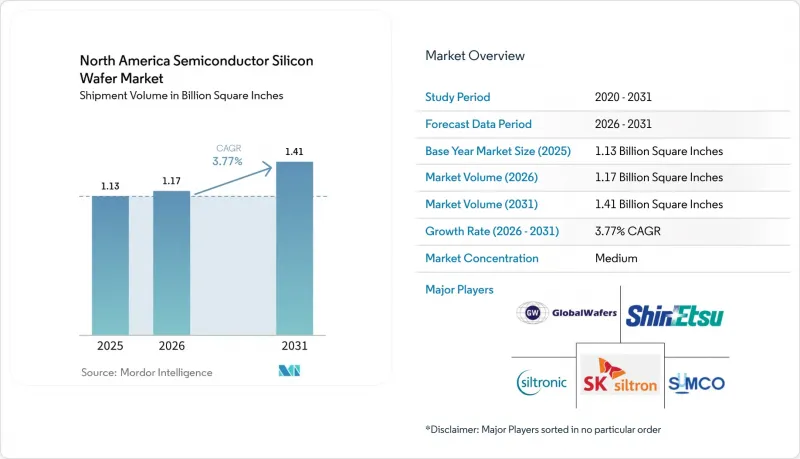
根據 Mordor Intelligence 預測,北美半導體矽晶圓市場(以出貨量為準)預計將從 2025 年的 11.3 億平方英寸成長到 2026 年的 11.7 億平方英寸,然後從 2026 年到 2031 年以 3.77% 的2031 年成長,到 17% 的複合年成長率。
本報告按晶圓直徑(150毫米及以下、200毫米、300毫米)、半導體裝置類型(邏輯元件、記憶體、模擬元件、分立元件等)、晶圓類型(拋光晶圓、外延晶圓、SOI晶圓、特種矽晶圓)、最終用戶(消費、工業、外延晶圓、SOI晶圓、特種矽晶圓)、最終用戶(家用電子電器、工業、區域通訊等。市場預測以體積(平方英吋)為單位。
北美半導體矽晶圓市場趨勢與洞察
主要鑄造廠擴大產能
台積電、德克薩斯和德州儀器的大規模多年投資持續推動北美半導體矽晶圓市場的發展。亞利桑那州的超級晶圓廠叢集的良率已達到與台灣相當的水平,英特爾的Fab 52工廠已開始採用18A工藝進行量產,德克薩斯也已在其Sherman工廠實現了人形機器人的自動化。集中的訂單使基板供應商能夠分攤認證成本並獲得預付款,從而確保可預測的產能和節點的快速量產。
美國《兒童健康保險流通與責任法案》(CHIPS Act)導致獎勵。
直接津貼、低利率貸款和25%的稅額扣抵抵免降低了從多晶矽到成品晶圓價值鏈各個環節的資本門檻。基於里程碑的付款方式可防止投機性過度建設,而償還條款則保護了納稅人的利益。晶圓製造商正利用這些補貼在其晶圓廠內建立配套設施,從而縮短物流週期,並增強北美半導體矽晶圓市場的供應韌性。
記憶體市場週期性低迷
通用DRAM和NAND快閃記憶體的持續庫存過剩導致2025年潔淨室空間佔用增加,但這並未轉化為晶圓需求的相應成長。長期合約以外的價格下跌正在擠壓晶圓供應商的利潤空間,使北美半導體矽晶圓市場面臨劇烈的季度波動。儘管人工智慧領域的高頻寬記憶體需求有所成長,但在庫存水準恢復正常之前,這不足以完全抵消需求下滑的影響。
細分市場分析
300毫米晶圓在北美半導體矽晶圓市場中佔比高達70.62%(按銷量計),並受益於尖端人工智慧和3奈米邏輯晶片量產的擴張。預計到2031年,其複合年成長率將達到4.95%。大晶片GPU、高密度DRAM和高度自動化的類比電路均受益於更大的晶圓面積,從而將光刻成本分攤到更多晶片上,並提升毛利率。因此,北美半導體矽晶圓市場中與300毫米晶圓廠相關的市場規模成長速度超過了整體市場成長速度,提高了供應商的需求可見度。
200mm晶圓在汽車、電力和成熟類比電路領域仍然至關重要,尤其是在電動車部署激增的背景下。安森美半導體和英飛凌生產線的增產確保了傳統晶圓廠的運作,避免了設備突然過時。同時提供兩種直徑晶圓的供應商正在緩解需求急劇下降的局面,並透過深化跨代裝置的合作關係,從長遠角度鞏固北美半導體矽晶圓市場。
到2025年,邏輯裝置的出貨量將佔總出貨量的33.09%,預計到2031年將以5.25%的複合年成長率成長,因為人工智慧推理技術正向智慧型手機、個人電腦和邊緣伺服器轉移。帶狀場效電晶體(RibbonFET)和背面供電技術提高了電晶體效率,但也提高了對晶體品質的要求。為這些節點供應晶圓的製造商獲得了溢價,從而提升了其在北美邏輯裝置相關半導體矽晶圓市場的佔有率。
儘管美國宣布將建造DRAM巨型晶圓廠,但記憶體週期性仍限制了其淨貢獻。高頻寬記憶體堆疊提高了每個封裝的矽晶圓用量,但來自個人電腦和行動電話的疲軟需求抑制了晶圓整體出貨量的成長。類比和分立元件的出貨量保持穩定,處於中等個位數成長水平,從而維持了面向工業和通訊客戶的基板供應商組合的平衡。
其他好處:
- Excel格式的市場預測(ME)表
- 3個月的分析師支持
目錄
第1章:引言
- 研究假設和市場定義
- 調查範圍
第2章:調查方法
第3章執行摘要
第4章 市場狀況
- 市場概覽
- 市場促進因素
- AI加速器製造廠對300毫米晶圓的需求激增。
- 《晶片製造和整合法案》(CHIPS Act)下的獎勵將促進國內晶圓生產。
- 電動車的快速普及正在推動對功率裝置用晶圓的需求。
- 向用於SiC和GaN裝置的特種矽過渡
- 邁向 2nm 節點的微型化藍圖:需要超平坦的優質晶圓。
- 回流措施旨在降低供應鏈風險
- 市場限制因素
- 多晶矽價格波動對供應商的利潤率帶來了壓力。
- 新建製造實驗室的環境許可核准流程變得越來越漫長。
- 與亞洲 300 毫米超大型晶圓廠的競爭限制了運轉率。
- 智慧型手機市場的放緩抑制了對傳統晶圓的需求。
- 產業價值鏈分析
- 監理情勢
- 宏觀經濟因素對市場的影響
- 技術展望
- 波特五力分析
第5章 市場規模與成長預測
- 依晶圓直徑
- 150毫米或更小
- 200 mm
- 300 mm
- 以半導體裝置類型分類
- 邏輯
- 記憶
- 模擬
- 離散的
- 其他半導體裝置(光電子裝置、感測器、微型元件)
- 依晶片類型
- 拋光
- 外延
- 絕緣體上矽(SOI)
- 特種矽(高電阻、高功率、感測器級)
- 最終用戶
- 家用電子產品
- 手機和智慧型手機
- 個人電腦和伺服器
- 產業
- 電訊
- 車
- 其他終端用戶應用程式
- 家用電子產品
- 國家
- 美國
- 加拿大
- 墨西哥
第6章 競爭情勢
- 市場集中度
- 策略趨勢
- 市佔率分析
- 公司簡介
- Shin-Etsu Chemical Co., Ltd.
- SUMCO Corporation
- GlobalWafers Co., Ltd.
- Siltronic AG
- SK Siltron Co., Ltd.
- Wafer Works Corporation
- Okmetic Oy
- Soitec SA
- Sil'Tronix Silicon Technologies
- SunEdison Semiconductor Ltd.
- Zhonghuan Semiconductor Co., Ltd.
- Simgui Technology Co., Ltd.
- Topsil Semiconductor Materials A/S
- Virginia Semiconductor Inc.
- Addison Engineering, Inc.
- University Wafer, Inc.
- Valley Design Corp.
- Pure Wafer PLC
- NOVA Electronic Materials, LLC
- Wafer World Inc.
第7章 市場機會與未來展望
According to Mordor Intelligence, the north america semiconductor silicon wafer market size in terms of shipment volume is expected to grow from 1.13 Billion Square Inches in 2025 to 1.17 Billion Square Inches in 2026 and is forecast to reach 1.41 Billion Square Inches by 2031 at a 3.77% CAGR over 2026-2031.
This report is Segmented by Wafer Diameter (Up To 150mm, 200mm, and 300mm), Semiconductor Device Type (Logic, Memory, Analog, Discrete, and More), Wafer Type (Prime Polished, Epitaxial, SOI, and Specialty Silicon), End-User (Consumer Electronics, Industrial, Telecommunications, and More), and Country. The Market Forecasts are Provided in Terms of Volume (Square Inches).
North America Semiconductor Silicon Wafer Market Trends and Insights
Capacity Expansions by Leading Foundries
Massive multiyear investments from TSMC, Intel, and Texas Instruments continue to upgrade the North America semiconductor silicon wafer market. The Arizona gigafab cluster already matches Taiwan yield levels, Intel's Fab 52 has entered high-volume production on 18A, and Texas Instruments has automated its Sherman complex with humanoid robots. Concentrated orders allow substrate suppliers to amortize qualification costs and lock in advance payments, ensuring predictable throughput and quicker node ramps.
Surge in U.S. CHIPS Act Incentives
Direct grants, low-cost loans, and a 25% tax credit lower capital hurdles for every tier of the value chain, from polysilicon to finished wafers. Milestone-based disbursements prevent speculative overbuilding, while clawback clauses protect taxpayers. Wafer makers leverage these subsidies to co-locate with fabs, shortening logistics cycles and enhancing supply resilience for the North America semiconductor silicon wafer market.
Cyclical Memory Downturns
A persistent inventory overhang in commodity DRAM and NAND used up cleanroom space without proportional wafer pull-through in 2025. Price erosion outside long-term contracts cut margins for wafer suppliers, exposing the North America semiconductor silicon wafer market to sharp quarterly swings. Although high-bandwidth memory for AI helps, it cannot fully neutralize volume softness until inventories normalize.
Other drivers and restraints analyzed in the detailed report include:
- Transition Toward 300 mm Wafers in Logic Nodes
- Rising Demand for Si Power Devices in EVs
- Supply Chain Geographic Concentration Risk
For complete list of drivers and restraints, kindly check the Table Of Contents.
Segment Analysis
The 300 mm slice of the North America semiconductor silicon wafer market stands at 70.62% volume and gains from leading-edge AI and 3 nm logic ramps, and expanding at a 4.95% CAGR through 2031. Large-die GPUs, high-density DRAM, and highly automated analog lines benefit from a larger surface, spreading lithography cost over more die and lifting gross margins. The North America semiconductor silicon wafer market size attached to 300 mm fabs therefore rises faster than the overall curve, reinforcing demand visibility for suppliers.
200 mm wafers remain crucial for automotive, power, and mature analog, particularly as EV content skyrockets. Capacity additions in onsemi and Infineon lines keep legacy fabs busy, preventing sudden obsolescence. Suppliers juggling both diameters offset demand cliffs and deepen relationships across device generations, which strengthens the North America semiconductor silicon wafer market over the long term.
Logic devices held 33.09% of the 2025 volume and are advancing at a 5.25% CAGR to 2031, as AI inference shifts to smartphones, PCs, and edge servers. RibbonFET and backside power delivery sharpen transistor efficiency, but they also raise crystal quality demands. Wafer makers shipping to these nodes capture price premiums, lifting the North America semiconductor silicon wafer market share tied to logic.
Memory's cyclicality tempers its net contribution despite U.S. DRAM megafab announcements. High-bandwidth memory stacks use more silicon per package, yet soft PC and handset demand restrains overall wafer lifts. Analog and discrete devices post steady, mid-single-digit volume growth, balancing the portfolio for substrates suppliers targeting industrial and telecom customers.
List of Companies Covered in this Report:
- Shin-Etsu Chemical Co., Ltd.
- SUMCO Corporation
- GlobalWafers Co., Ltd.
- Siltronic AG
- SK Siltron Co., Ltd.
- Wafer Works Corporation
- Okmetic Oy
- Soitec SA
- Sil'Tronix Silicon Technologies
- SunEdison Semiconductor Ltd.
- Zhonghuan Semiconductor Co., Ltd.
- Simgui Technology Co., Ltd.
- Topsil Semiconductor Materials A/S
- Virginia Semiconductor Inc.
- Addison Engineering, Inc.
- University Wafer, Inc.
- Valley Design Corp.
- Pure Wafer PLC
- NOVA Electronic Materials, LLC
- Wafer World Inc.
Additional Benefits:
- The market estimate (ME) sheet in Excel format
- 3 months of analyst support
TABLE OF CONTENTS
1 INTRODUCTION
- 1.1 Study Assumptions and Market Definition
- 1.2 Scope of the Study
2 RESEARCH METHODOLOGY
3 EXECUTIVE SUMMARY
4 MARKET LANDSCAPE
- 4.1 Market Overview
- 4.2 Market Drivers
- 4.2.1 Soaring Demand for 300 mm Wafers from AI Accelerator Fabs
- 4.2.2 CHIPS Act Incentives Catalyzing Local Wafer Production
- 4.2.3 Rapid Adoption of Electric Vehicles Boosting Power Device Wafers
- 4.2.4 Transition Toward Specialty Silicon for SiC and GaN Devices
- 4.2.5 Miniaturization Roadmap to 2 nm Nodes Requiring Ultra-Flat Prime Wafers
- 4.2.6 Reshoring Initiatives Reducing Supply-Chain Risk
- 4.3 Market Restraints
- 4.3.1 Volatile Polysilicon Prices Squeezing Supplier Margins
- 4.3.2 Lengthy Environmental Permitting Delays for New Fabs
- 4.3.3 Competition from Asian 300 mm Megafabs Limiting Utilization
- 4.3.4 Smartphone Market Slowdown Dampening Legacy Wafer Demand
- 4.4 Industry Value Chain Analysis
- 4.5 Regulatory Landscape
- 4.6 Impact of Macroeconomic Factors on the Market
- 4.7 Technological Outlook
- 4.8 Porter's Five Forces Analysis
- 4.8.1 Bargaining Power of Suppliers
- 4.8.2 Bargaining Power of Buyers
- 4.8.3 Threat of New Entrants
- 4.8.4 Threat of Substitutes
- 4.8.5 Intensity of Competitive Rivalry
5 MARKET SIZE AND GROWTH FORECASTS (VOLUME)
- 5.1 By Wafer Diameter
- 5.1.1 Up to 150 mm
- 5.1.2 200 mm
- 5.1.3 300 mm
- 5.2 By Semiconductor Device Type
- 5.2.1 Logic
- 5.2.2 Memory
- 5.2.3 Analog
- 5.2.4 Discrete
- 5.2.5 Other Semiconductor Device Types (Optoelectronics, Sensors, Micro)
- 5.3 By Wafer Type
- 5.3.1 Prime Polished
- 5.3.2 Epitaxial
- 5.3.3 Silicon-on-Insulator (SOI)
- 5.3.4 Specialty Silicon (High-Resistivity, Power, Sensor-Grade)
- 5.4 By End-user
- 5.4.1 Consumer Electronics
- 5.4.1.1 Mobile and Smartphones
- 5.4.1.2 PCs and Servers
- 5.4.2 Industrial
- 5.4.3 Telecommunications
- 5.4.4 Automotive
- 5.4.5 Other End-user Applications
- 5.4.1 Consumer Electronics
- 5.5 By Country
- 5.5.1 United States
- 5.5.2 Canada
- 5.5.3 Mexico
6 COMPETITIVE LANDSCAPE
- 6.1 Market Concentration
- 6.2 Strategic Moves
- 6.3 Market Share Analysis
- 6.4 Company Profiles (includes Global Level Overview, Market Level Overview, Core Segments, Financials as available, Strategic Information, Market Rank/Share, Products and Services, Recent Developments)
- 6.4.1 Shin-Etsu Chemical Co., Ltd.
- 6.4.2 SUMCO Corporation
- 6.4.3 GlobalWafers Co., Ltd.
- 6.4.4 Siltronic AG
- 6.4.5 SK Siltron Co., Ltd.
- 6.4.6 Wafer Works Corporation
- 6.4.7 Okmetic Oy
- 6.4.8 Soitec SA
- 6.4.9 Sil'Tronix Silicon Technologies
- 6.4.10 SunEdison Semiconductor Ltd.
- 6.4.11 Zhonghuan Semiconductor Co., Ltd.
- 6.4.12 Simgui Technology Co., Ltd.
- 6.4.13 Topsil Semiconductor Materials A/S
- 6.4.14 Virginia Semiconductor Inc.
- 6.4.15 Addison Engineering, Inc.
- 6.4.16 University Wafer, Inc.
- 6.4.17 Valley Design Corp.
- 6.4.18 Pure Wafer PLC
- 6.4.19 NOVA Electronic Materials, LLC
- 6.4.20 Wafer World Inc.
7 MARKET OPPORTUNITIES AND FUTURE OUTLOOK
- 7.1 White-Space and Unmet-Need Assessment
 矽晶圓市場-全球產業規模、佔有率、趨勢、機會和預測:按晶圓尺寸、類型、應用、最終用戶、地區和競爭格局分類,2021-2031年
 300mm矽晶圓:市場佔有率分析、產業趨勢與統計、成長預測(2026-2031年)美國半導體矽晶圓:市場佔有率分析、行業趨勢和統計數據以及成長預測(2026-2031 年)
 矽晶圓市場規模、佔有率、趨勢和預測:按晶圓尺寸、類型、應用、最終用途和地區分類,2026-2034 年
 半導體矽晶圓回收市場:依回收製程、晶圓類型、晶圓尺寸、應用領域、產業及最終用戶分類-2026-2032年全球市場預測
 2026-2034年全球太陽能矽晶圓市場規模、佔有率、趨勢和成長分析報告5G半導體矽晶圓:市場佔有率分析、產業趨勢與統計及成長預測(2026-2031年)工業半導體矽晶圓:市場佔有率分析、產業趨勢與統計、成長預測(2026-2031)用於功率元件的矽晶圓:市場佔有率分析、行業趨勢和統計數據以及成長預測(2026-2031 年)高阻矽晶圓:市佔率分析、產業趨勢與統計、成長預測(2026-2031 年)