

 |
市場調查報告書
商品編碼
2063398
300mm矽晶圓:市場佔有率分析、產業趨勢與統計、成長預測(2026-2031年)300mm Silicon Wafer - Market Share Analysis, Industry Trends & Statistics, Growth Forecasts (2026 - 2031) |
||||||
※ 本網頁內容可能與最新版本有所差異。詳細情況請與我們聯繫。
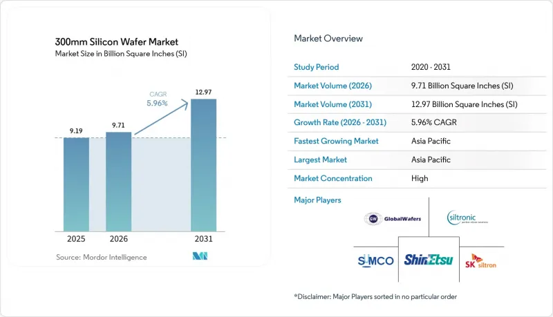
根據 Mordor Intelligence 預測,300 毫米矽晶圓的市場規模預計將在 2025 年達到 91.9 億平方英寸,在 2026 年達到 97.1 億平方英寸,並在 2031 年達到 129.7 億平方英寸。
預計從 2026 年到 2031 年,其複合年成長率將達到 5.96%。
本報告按半導體裝置類型(邏輯裝置、記憶體、類比元件、分立元件、功率元件及其他)、晶圓類型(原晶圓、拋光晶圓、外延晶圓、絕緣體上矽 (SOI) 晶圓、特種矽晶圓)、終端使用者應用(消費性裝置上矽 (SOI) 晶圓、特種矽晶圓)、終端使用者應用(消費性、工業、通訊、汽車及其他)和地區進行通訊、汽車及其他)和終端使用者應用(消費性、工業、通訊、汽車及其他)和地區進行通訊。市場預測以出貨面積(十億平方英吋)為單位。
全球300毫米矽晶圓市場趨勢及洞察
先進節點對邏輯和儲存裝置的需求不斷成長
隨著2nm製程和高頻寬記憶體生產線的量產,晶圓開片量不斷增加。這是因為隨著製程節點的小型化,光罩層厚度增加,缺陷容許度也更加嚴格。台積電計畫於2026年下半年開始量產其2nm平台,與同等3nm產品相比,單晶片晶圓面積將增加15%。美光的HBM4產能將持續滿載運轉至2026年,而SK海力士正在擴大12層堆疊HBM3E的產能,其所需的晶圓面積比傳統產品增加50%。三星的目標是到2026年底,其2nm製程的月開片量達到21,000片,而英特爾則計劃在2026年中期獲得其18A製程的外部客戶認證。目前,多年期基板供應合約在採購市場佔據主導地位,這增強了現有製造商相對於無晶圓廠設計公司的定價權。
亞太地區鑄造產能擴張
台積電計畫在台灣、美國和日本共投資1,650億美元,到2029年每月新增約120萬片300毫米晶圓產能。三星計劃在2030年為其位於韓國的巨型晶圓廠投資300兆韓元(約2,300億美元)。儘管面臨製造設備出口限制,中芯國際位於北京的生產線仍計劃在其成熟節點上每月生產10萬片晶圓。將在歐洲德勒斯登成立的合資企業,投資額達100億歐元(約113億美元),將於2027年開始每月生產4萬片晶圓。晶圓供應商正在這些工廠附近選址,例如Siltronic在新加坡投資20億歐元(約22.6億美元)的工廠。由於外延坯料的前置作業時間長達18個月,提前確保產能變得至關重要。
擴大300毫米晶圓廠的資本投資
由於每套EUV光刻設備造價高達1.5億至2億美元,3奈米及以下製程的待開發區工廠建設成本現已超過150億美元。台積電位於亞利桑那州的專案預算甚至超過400億美元,原因是勞動力成本高昂以及美國授權延遲。英特爾位於俄亥俄州的項目到2030年可能需要1000億美元,但《晶片法案》(CHIPS Act)的補貼僅佔總支出的個位數百分比。高資本密集度導致了壟斷市場結構,新進入者僅限於政府支持和垂直整合的公司。如果人工智慧需求放緩,產能運轉率下降的風險可能會加重營運商的資產負債表負擔。
細分市場分析
預計到2025年,邏輯裝置的出貨量將佔總出貨量的43.76%,隨著2nm環柵(GaA)電晶體的量產,這一佔有率預計還將進一步成長。在300mm矽晶圓市場中,邏輯元件預計將是成長最快的。這是因為隨著晶片尺寸的縮小,每個成品晶片所需的光刻掩模和晶圓起始數量都會增加。高頻寬記憶體(HBM)正在推動記憶體市場佔有率的成長,但邏輯元件領域仍然普遍存在多年期供貨契約,這使得大型代工廠受現貨市場供不應求的影響較小。
預計到2025年,記憶體將佔出貨量的約35%,由於垂直堆疊技術,每種HBM變體的面積都會增加。類比和混合訊號裝置將佔約12%,它們正從200mm晶圓轉向300mm晶圓以提高良率和降低成本。同時,佔6%的離散式功率半導體正轉向300mm晶圓以滿足電動車應用的需求。小眾光電子裝置和MEMS合計佔比不到4%,但在汽車LiDAR和生物識別感測器領域正迅速發展。因此,儘管300mm矽晶圓市場主要集中在邏輯半導體領域,但廣泛的產品多元化確保了產能的均衡利用。
區域分析
到2025年,亞太地區將佔全球出貨量的79.67%,這主要得益於台灣每月300萬片晶圓的量產以及韓國在記憶體領域的主導地位。具有競爭力的電價、密集的供應商叢集以及強力的公共支持,將推動以該地區為中心的300毫米矽晶圓市場在2031年前以6.06%的複合年成長率成長。在中國,儘管出口限制依然存在,但成熟製程節點的成長帶動了市場佔有率的擴大。在日本,熊本和Rapidus計畫正協助該地區重振市場,並獲得了2兆日圓(約130億美元)的獎勵支持。
預計到2025年,北美將佔全球半導體產量的約10%,《晶片法案》(CHIPS Act)的資金正在加速亞利桑那州、俄亥俄州和愛達荷州的建設。然而,由於勞動力和授權壁壘,北美的發展落後於亞洲。歐洲目前約佔全球半導體產量的7%,並計劃透過一項430億歐元(約486億美元)的公私合作項目,到2030年將其佔比提高到20%。高昂的能源成本和監管差異仍然是實施過程中面臨的挑戰。
預計到2025年,南美、中東和非洲的市佔率總和將低於3%。儘管沙烏地阿拉伯和阿拉伯聯合大公國的資本項目顯示市場需求日益成長,但由於缺乏成熟的供應商生態系統,短期內產能擴張受到限制。因此,亞太地區的供應中斷會波及全球,凸顯了300毫米矽晶圓市場持續存在的區域集中度。
其他好處
- Excel格式的市場預測(ME)表
- 3個月的分析師支持
目錄
第1章:引言
- 研究假設和市場定義
- 調查範圍
第2章:調查方法
第3章執行摘要
第4章 市場狀況
- 市場概覽
- 市場促進因素
- 先進節點對邏輯和儲存裝置的需求不斷成長
- 亞太地區鑄造產能擴張
- 加大對人工智慧、高效能運算和資料中心的投資
- 採用背面供電和3D IC封裝
- 政府對國內晶圓供應鏈的補貼
- 異構整合加速了300mm晶圓的應用。
- 市場限制因素
- 擴大對300毫米晶圓廠的資本投資
- 多晶矽和設備供應鏈中的脆弱性
- 過渡到直徑超過 300 毫米的管道所面臨的技術障礙
- 高能耗製造業引發了人們對永續性。
- 產業價值鏈分析
- 監理情勢
- 技術展望
- 宏觀經濟因素對市場的影響
- 波特五力分析
第5章 市場規模及成長預測(按地區分類的出貨量)
- 依半導體裝置類型
- 邏輯
- 記憶
- 模擬
- 分立和功率
- 其他半導體裝置(光電子裝置、感測器、微型元件)
- 依晶片類型
- 主要的
- 拋光
- 外延
- 絕緣體上矽(SOI)
- 特種矽(高電阻、高功率、感測器級)
- 透過最終用戶應用程式
- 家用電器
- 行動裝置和智慧型手機
- PC和伺服器
- 工業的
- 溝通
- 車
- 其他終端用戶應用程式
- 家用電器
- 按地區
- 北美洲
- 美國
- 加拿大
- 墨西哥
- 歐洲
- 德國
- 英國
- 法國
- 其他歐洲國家
- 亞太地區
- 中國
- 日本
- 印度
- 韓國
- 台灣
- 其他亞太國家
- 南美洲
- 中東和非洲
- 北美洲
第6章 競爭情勢
- 市場集中度
- 策略趨勢
- 市佔率分析
- 公司簡介
- SUMCO Corporation
- Shin-Etsu Chemical Co., Ltd.
- GlobalWafers Co., Ltd.
- Siltronic AG
- SK Siltron Co., Ltd.
- Okmetic Oyj
- WaferWorks Corporation
- RS Technologies Co., Ltd.
- ESWIN Materials Co., Ltd.
- Topsil Semiconductor Materials A/S
- LONGi Silicon Materials Corp.
- Gritek Solar Silicon Industry Co., Ltd.
- Poshing Silicon Co., Ltd.
- LX Semicon Co., Ltd.
- Panzhihua Dingxin Electronic Silicon Co., Ltd.
- Jiangsu Zhongneng Silicon Technology Development Co., Ltd.
- PV Crystalox Silicon GmbH
第7章 市場機會與未來展望
According to Mordor Intelligence, the 300mm silicon wafer market size is projected to be 9.19 billion square inches in 2025, 9.71 billion square inches in 2026, and reach 12.97 billion square inches by 2031, growing at a 5.96% CAGR from 2026 to 2031.
This report is Segmented by Semiconductor Device Type (Logic, Memory, Analog, Discrete and Power, and More), Wafer Type (Prime Polished, Epitaxial, Silicon-On-Insulator (SOI), and Specialty Silicon), End-User Application (Consumer Electronics, Industrial, Telecommunications, Automotive, and More), and Geography. The Market Forecasts are Provided in Terms of Shipment Area (Billion Square Inches).
Global 300mm Silicon Wafer Market Trends and Insights
Rising Demand For Advanced Node Logic And Memory Devices
Volume ramps at 2-nanometer and high-bandwidth memory lines elevate wafer starts because each node shrink adds reticle layers and tighter defect budgets. TSMC aims for late-2026 volume on its 2 nm platform, consuming 15% more wafer area per chip than 3 nm equivalents. Micron's HBM4 capacity remains fully booked through 2026, while SK Hynix scales 12-high HBM3E stacks that require 50% extra wafer surface versus conventional. Samsung targets 21,000 wafer starts per month at 2 nm by end-2026, and Intel pursues 18A qualification for external customers in mid-2026. Multi-year substrate agreements now dominate procurement, boosting incumbents' pricing leverage over fabless designers.
Expansion Of Foundry Capacities In Asia-Pacific
TSMC has earmarked USD 165 billion across Taiwan, the United States, and Japan, adding roughly 1.2 million monthly 300 mm starts by 2029. Samsung plans KRW 300 trillion (USD 230 billion) for South Korean megafabs through 2030. SMIC's Beijing line seeks 100,000 starts monthly at mature nodes despite tool controls. Europe's Dresden joint venture, backed by EUR 10 billion (USD 11.3 billion), brings 40,000 starts a month beginning 2027. Wafer suppliers co-locate near these hubs, as shown by Siltronic's EUR 2 billion (USD 2.26 billion) Singapore plant. Rising lead times of up to 18 months for epitaxial blanks reinforce capacity pre-commitment.
Escalating Capital Expenditure For 300 mm Fabs
A sub-3 nm greenfield facility now exceeds USD 15 billion, driven by EUV tool sets priced at USD 150 million to USD 200 million apiece. TSMC's Arizona budget rose from USD 40 billion to higher levels because of U.S. labor rates and permitting delays. Intel's Ohio project may need USD 100 billion through 2030, while CHIPS Act subsidies cover only single-digit percentages of total outlays. High capital intensity confines new entry to state-backed or vertically integrated firms, embedding oligopolistic market structure. Should AI demand falter, underutilization risks amplify balance-sheet stress for operators.
Other drivers and restraints analyzed in the detailed report include:
- Proliferation Of AI, HPC And Data-Center Investments
- Adoption Of Backside Power Delivery And 3D IC Packaging
- Supply Chain Vulnerabilities In Polysilicon And Equipment
For complete list of drivers and restraints, kindly check the Table Of Contents.
Segment Analysis
Logic devices controlled 43.76% of shipments in 2025, and this share climbs as 2 nm gate-all-around transistors reach mass production. The 300mm silicon wafer market size allocated to logic is projected to grow fastest because each shrink raises reticle count and wafer starts per finished die. High-bandwidth memory boosts memory's surface share but logic still commands supply contracts that span several years, insulating leading foundries from spot shortages.
Memory held about 35% of 2025 shipments, with HBM variants consuming more area due to vertical stacking. Analog and mixed-signal devices represent roughly 12%, migrating from 200 mm for yield and cost benefits, while discrete power semiconductors at 6% shift to 300 mm to serve electric vehicles. Niche optoelectronics and MEMS together remain below 4% but gain momentum in automotive lidar and biometric sensors. The 300mm silicon wafer market therefore pivots around logic intensity, but broader diversification ensures balanced capacity utilization.
Geography Analysis
Asia-Pacific retained 79.67% of shipments in 2025, anchored by Taiwan's 3 million monthly starts and South Korea's memory leadership. The 300mm silicon wafer market size centered in this region is slated for a 6.06% CAGR through 2031, thanks to competitive electricity rates, dense supplier clusters, and committed public incentives. China's mature-node expansions lift its participation despite ongoing export controls. Japan re-emerges through Kumamoto and Rapidus programs backed by JPY 2 trillion (USD 13.0 billion) incentives.
North America contributed nearly 10% in 2025, with CHIPS Act funding accelerating builds in Arizona, Ohio, and Idaho. However, labor and permitting hurdles slow realization relative to Asia. Europe held roughly 7%, and seeks 20% of global semiconductor output by 2030 via EUR 43 billion (USD 48.6 billion) public-private financingU. Higher energy costs and regulatory diversity remain execution challenges.
South America and the Middle East and Africa together captured less than 3% in 2025. While capital projects in Saudi Arabia and the United Arab Emirates hint at nascent interest, the lack of established supplier ecosystems constrains near-term volume. Consequently, any supply disruption in Asia-Pacific reverberates globally, underscoring persistent regional concentration within the 300mm silicon wafer market.
- SUMCO Corporation
- Shin-Etsu Chemical Co., Ltd.
- GlobalWafers Co., Ltd.
- Siltronic AG
- SK Siltron Co., Ltd.
- Okmetic Oyj
- WaferWorks Corporation
- RS Technologies Co., Ltd.
- ESWIN Materials Co., Ltd.
- Topsil Semiconductor Materials A/S
- LONGi Silicon Materials Corp.
- Gritek Solar Silicon Industry Co., Ltd.
- Poshing Silicon Co., Ltd.
- LX Semicon Co., Ltd.
- Panzhihua Dingxin Electronic Silicon Co., Ltd.
- Jiangsu Zhongneng Silicon Technology Development Co., Ltd.
- PV Crystalox Silicon GmbH
Additional Benefits:
- The market estimate (ME) sheet in Excel format
- 3 months of analyst support
TABLE OF CONTENTS
1 INTRODUCTION
- 1.1 Study Assumptions and Market Definition
- 1.2 Scope of the Study
2 RESEARCH METHODOLOGY
3 EXECUTIVE SUMMARY
4 MARKET LANDSCAPE
- 4.1 Market Overview
- 4.2 Market Drivers
- 4.2.1 Rising Demand for Advanced Node Logic and Memory Devices
- 4.2.2 Expansion of Foundry Capacities in Asia-Pacific
- 4.2.3 Proliferation of AI, HPC, and Data-Center Investments
- 4.2.4 Adoption of Backside Power Delivery and 3D IC Packaging
- 4.2.5 Government Subsidies for Domestic Wafer Supply Chains
- 4.2.6 Heterogeneous Integration Accelerating 300 mm Wafer Utilization
- 4.3 Market Restraints
- 4.3.1 Escalating Capital Expenditure for 300 mm Fabs
- 4.3.2 Supply Chain Vulnerabilities in Polysilicon and Equipment
- 4.3.3 Technical Barriers to Transition Beyond 300 mm Diameter
- 4.3.4 Energy-Intensive Manufacturing Raising Sustainability Concerns
- 4.4 Industry Value Chain Analysis
- 4.5 Regulatory Landscape
- 4.6 Technological Outlook
- 4.7 Impact of Macroeconomic Factors on the Market
- 4.8 Porter's Five Forces Analysis
- 4.8.1 Bargaining Power of Suppliers
- 4.8.2 Bargaining Power of Buyers
- 4.8.3 Threat of New Entrants
- 4.8.4 Threat of Substitutes
- 4.8.5 Competitive Rivalry
5 MARKET SIZE AND GROWTH FORECASTS (SHIPMENT IN AREA)
- 5.1 By Semiconductor Device Type
- 5.1.1 Logic
- 5.1.2 Memory
- 5.1.3 Analog
- 5.1.4 Discrete and Power
- 5.1.5 Other Semiconductor Device Types (Optoelectronics, Sensors, Micro)
- 5.2 By Wafer Type
- 5.2.1 Prime
- 5.2.2 Polished
- 5.2.3 Epitaxial
- 5.2.4 Silicon-on-Insulator (SOI)
- 5.2.5 Specialty Silicon (High-Resistivity, Power, Sensor-Grade)
- 5.3 By End-user Application
- 5.3.1 Consumer Electronics
- 5.3.1.1 Mobile and Smartphones
- 5.3.1.2 PCs and Servers
- 5.3.2 Industrial
- 5.3.3 Telecommunications
- 5.3.4 Automotive
- 5.3.5 Other End-user Applications
- 5.3.1 Consumer Electronics
- 5.4 By Geography
- 5.4.1 North America
- 5.4.1.1 United States
- 5.4.1.2 Canada
- 5.4.1.3 Mexico
- 5.4.2 Europe
- 5.4.2.1 Germany
- 5.4.2.2 United Kingdom
- 5.4.2.3 France
- 5.4.2.4 Rest of Europe
- 5.4.3 Asia-Pacific
- 5.4.3.1 China
- 5.4.3.2 Japan
- 5.4.3.3 India
- 5.4.3.4 South Korea
- 5.4.3.5 Taiwan
- 5.4.3.6 Rest of Asia-Pacific
- 5.4.4 South America
- 5.4.5 Middle East and Africa
- 5.4.1 North America
6 COMPETITIVE LANDSCAPE
- 6.1 Market Concentration
- 6.2 Strategic Moves
- 6.3 Market Share Analysis
- 6.4 Company Profiles (includes Global Level Overview, Market Level Overview, Core Segments, Financials as available, Strategic Information, Market Rank/Share, Products and Services, Recent Developments)
- 6.4.1 SUMCO Corporation
- 6.4.2 Shin-Etsu Chemical Co., Ltd.
- 6.4.3 GlobalWafers Co., Ltd.
- 6.4.4 Siltronic AG
- 6.4.5 SK Siltron Co., Ltd.
- 6.4.6 Okmetic Oyj
- 6.4.7 WaferWorks Corporation
- 6.4.8 RS Technologies Co., Ltd.
- 6.4.9 ESWIN Materials Co., Ltd.
- 6.4.10 Topsil Semiconductor Materials A/S
- 6.4.11 LONGi Silicon Materials Corp.
- 6.4.12 Gritek Solar Silicon Industry Co., Ltd.
- 6.4.13 Poshing Silicon Co., Ltd.
- 6.4.14 LX Semicon Co., Ltd.
- 6.4.15 Panzhihua Dingxin Electronic Silicon Co., Ltd.
- 6.4.16 Jiangsu Zhongneng Silicon Technology Development Co., Ltd.
- 6.4.17 PV Crystalox Silicon GmbH
7 MARKET OPPORTUNITIES AND FUTURE OUTLOOK
- 7.1 White-space and Unmet-Need Assessment
 矽晶圓市場-全球產業規模、佔有率、趨勢、機會和預測:按晶圓尺寸、類型、應用、最終用戶、地區和競爭格局分類,2021-2031年
 北美半導體矽晶圓:市場佔有率分析、產業趨勢與統計及成長預測(2026-2031 年)美國半導體矽晶圓:市場佔有率分析、行業趨勢和統計數據以及成長預測(2026-2031 年)
 矽晶圓市場規模、佔有率、趨勢和預測:按晶圓尺寸、類型、應用、最終用途和地區分類,2026-2034 年
 半導體矽晶圓回收市場:依回收製程、晶圓類型、晶圓尺寸、應用領域、產業及最終用戶分類-2026-2032年全球市場預測
 2026-2034年全球太陽能矽晶圓市場規模、佔有率、趨勢和成長分析報告5G半導體矽晶圓:市場佔有率分析、產業趨勢與統計及成長預測(2026-2031年)工業半導體矽晶圓:市場佔有率分析、產業趨勢與統計、成長預測(2026-2031)用於功率元件的矽晶圓:市場佔有率分析、行業趨勢和統計數據以及成長預測(2026-2031 年)高阻矽晶圓:市佔率分析、產業趨勢與統計、成長預測(2026-2031 年)