

 |
市場調查報告書
商品編碼
2063401
美國半導體矽晶圓:市場佔有率分析、行業趨勢和統計數據以及成長預測(2026-2031 年)United States Semiconductor Silicon Wafer - Market Share Analysis, Industry Trends & Statistics, Growth Forecasts (2026 - 2031) |
||||||
※ 本網頁內容可能與最新版本有所差異。詳細情況請與我們聯繫。
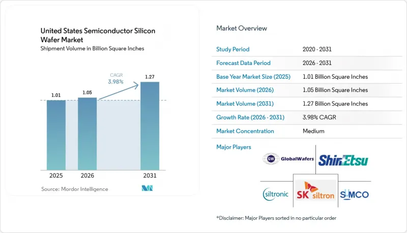
根據 Mordor Intelligence 預測,美國半導體矽晶圓市場規模(以出貨量為準)預計到 2025 年將達到 10.1 億平方英寸,到 2026 年將達到 10.5 億平方英寸,到 2031 年將達到 12.7 億平方英寸,2026 年的複合年成長率為 203.389%。
本報告按晶圓直徑(150毫米及以下、200毫米、300毫米)、半導體裝置類型(邏輯裝置、記憶體、類比元件、分立元件及其他)、晶圓類型(拋光晶圓、外延晶圓、SOI晶圓、特種矽晶圓)以及最終用戶(消費晶圓、外延晶圓、SOI晶圓、特種矽晶圓)以及最終用戶(消費晶圓、工業、細分市場及其他,包括行動裝置進行細分市場。市場預測以體積(平方英吋)為單位。
美國半導體矽晶圓市場的趨勢與洞察
主要鑄造廠擴大產能
全球三大半導體公司前所未有的資本投資正在重塑美國半導體矽晶圓市場格局。台積電已在亞利桑那州建成六座巨型晶圓廠和兩條先進封裝生產線;英特爾正在四個州新增18A生產線;三星則在德克薩斯州擴建其2奈米邏輯晶片園區。每座工廠一旦全面運作,每年將消耗數百萬片300毫米晶圓。美國本土基板工廠將不得不依賴進口。
美國《CHIPS法案》下的獎勵激增
《晶片科學法案》降低了新建工廠的進入門檻,並已將原本可能流向亞洲的投資轉移到了美國。配套津貼使美國晶圓生產線的實際成本降低了高達五分之一,該法案還包含嚴格的規定,將在未來十年內阻止中國先進製程節點的擴張。雖然這些措施將維持國內的額外需求,但供應穩定性問題僅部分解決,因為多晶矽這種原料仍需從德國和日本進口。
記憶體市場週期性低迷
2025年初,由於智慧型手機銷售放緩以及雲端服務公司調整庫存,DRAM和NAND快閃供應商大幅削減了訂單。由於儲存晶圓幾乎占美國半導體矽晶圓市場的四分之一,即使是單次價格調整也可能導致基板銷售迅速下滑。雖然用於人工智慧伺服器的高頻寬記憶體需求依然強勁,但其細分市場規模太小,不足以穩定整體需求。
細分市場分析
預計到2025年,300毫米晶圓在美國半導體矽晶圓市場的佔有率將達到70.62%(按銷量計),並在2031年之前以4.95%的複合年成長率持續成長。僅台積電和英特爾在亞利桑那州和俄亥俄州新建的晶圓廠,預計全面運作後將新增超過3,000萬平方英吋的需求。雖然每片晶圓上更高的晶片數量可以提高成本效益,但目前全球僅有三家供應商佔據了300毫米矽晶圓產能的顯著佔有率。
相較之下,200mm基板是類比電路、MEMS 和汽車電力電子裝置的基礎。雖然這種尺寸規格在 2023 年至 2026 年間成長了 14%,但美國的產能僅佔全球供應量的 14%。由於逆變器晶片和工業控制晶片對同一晶圓展開競爭,汽車製造商在 2026 年至 2027 年間可能面臨供不應求。 150mm 以下尺寸的晶圓仍在國防領域和傳統產品線中使用,但其年成長率僅為 1.8%,這進一步加劇了供應結構呈現三速運轉的局面,迫使晶圓製造商將投資集中於既能提供充足產量又能帶來豐厚利潤的領域。
預計到2025年,邏輯半導體將占美國半導體矽晶圓市場佔有率的33.09%,並將在2031年之前以5.25%的複合年成長率持續成長,這主要得益於人工智慧(AI)加速器對尖端製程節點和外延層的需求。台積電透露,其3奈米製程的銷量在2025年下半年超過了智慧型手機的銷量,印證了高效能運算(HPC)的強勁發展勢頭。
同時,由於DRAM和NAND價格走軟,記憶體產量在2025年初有所下降。用於訓練叢集的HBM元件仍然盈利,但其在記憶體晶圓產量中所佔比例不到5%。 200毫米晶圓廠的類比和分立元件產量維持3-4%的穩定成長,而感測器和MEMS元件的產量也維持著類似的成長速度,這主要得益於汽車雷達和智慧音箱的需求。
其他好處
- Excel格式的市場預測(ME)表
- 3個月的分析師支持
目錄
第1章:引言
- 研究假設和市場定義
- 調查範圍
第2章:調查方法
第3章執行摘要
第4章 市場狀況
- 市場概覽
- 市場促進因素
- 主流趨勢:大型鑄造廠擴大產能
- 主流趨勢:美國《兒童健康保險計劃法案》(CHIPS Act)下的獎勵激增
- 主流趨勢:邏輯節點向 300 毫米晶圓過渡。
- 主流趨勢:電動車中的矽功率裝置及不斷成長的需求
- 對人工智慧最佳化型SOI晶圓的潛在需求尚未被察覺
- 不易察覺的、國防級抗輻射矽
- 市場限制因素
- 主流記憶與循環記憶衰退
- 主流供應鏈地理集中風險
- 晶體缺陷尺寸小於 3 nm 的極限常被忽視
- SiC基板和GaN基板之間的競爭正在暗中加劇。
- 產業價值鏈分析
- 監理情勢
- 技術分析
- 宏觀經濟因素的影響
- 波特五力分析
第5章 市場規模與成長預測
- 依晶圓直徑
- 150毫米或更小
- 200mm
- 300mm
- 依半導體裝置類型
- 邏輯
- 記憶
- 模擬
- 離散的
- 其他半導體裝置(光電子裝置、感測器、微型元件)
- 依晶片類型
- 拋光
- 外延
- 絕緣體上矽(SOI)
- 特種矽(高電阻、高功率、感測器級)
- 最終用戶
- 家用電器
- 手機和智慧型手機
- PC 和伺服器
- 工業的
- 用於溝通
- 車
- 其他
- 家用電器
第6章 競爭情勢
- 市場集中度
- 策略趨勢
- 市佔率分析
- 公司簡介
- Shin-Etsu Chemical Co., Ltd.
- SUMCO Corporation
- GlobalWafers Co., Ltd.
- Siltronic AG
- SK siltron Co., Ltd.
- Okmetic Oy
- Wafer Works Corp.
- Siltronic Silicon Wafer Pte Ltd
- Soitec SA
- WaferPro
- Tianjin Zhonghuan Semiconductor Co., Ltd.
- Ultrasil Corporation
- Poshing Technology Co., Ltd.
- Advanced Silicon Technologies
- 300mm Wafer Fab LLC
- Virginia Semiconductor, Inc.
- Rogue Valley Microdevices, Inc.
- SKC Solmics Co., Ltd.
- Qromis, Inc.
- Addison Engineering, Inc.
第7章 市場機會與未來展望
According to Mordor Intelligence, the united states semiconductor silicon wafer market size in terms of shipment volume is projected to be 1.01 Billion Square Inches in 2025, 1.05 Billion Square Inches in 2026, and reach 1.27 Billion Square Inches by 2031, growing at a CAGR of 3.98% from 2026 to 2031.
This report is Segmented by Wafer Diameter (Up To 150mm, 200mm, 300mm), Semiconductor Device Type (Logic, Memory, Analog, Discrete, Other), Wafer Type (Prime Polished, Epitaxial, SOI, Specialty Silicon), and End-User (Consumer Electronics With Mobile and PCs Subsegments, Industrial, Telecommunications, and More). The Market Forecasts are Provided in Terms of Volume (Square Inches).
United States Semiconductor Silicon Wafer Market Trends and Insights
Capacity Expansions by Leading Foundries
Unprecedented capital spending by three global leaders is reshaping the United States semiconductor silicon wafer market. TSMC is installing six mega-fabs and two advanced packaging lines in Arizona, Intel is adding new 18A lines across four states, and Samsung is scaling a two-nanometer logic campus in Texas. Each site will consume millions of 300 millimeter wafers every year once fully qualified. Domestic substrate makers are racing to match that pull, but new crystal-growth and slicing workshops will not reach steady output until 2027, which leaves a two-year window in which foundries remain tied to imports.
Surge in U.S. CHIPS Act Incentives
The CHIPS and Science Act lowers the hurdle rate for new plants and has already redirected investments that might have gone to Asia. Matching grants cut the effective cost of a United States wafer line by as much as a fifth and include hard guardrails that block advanced-node expansion in China for a decade. Those terms keep incremental demand local, yet raw polysilicon still arrives from Germany or Japan, meaning supply security is only partially solved.
Cyclical Memory Downturns
DRAM and NAND suppliers cut orders sharply in early 2025 as smartphone sales softened and cloud firms digested inventory. Memory wafers represent nearly one-quarter of the United States semiconductor silicon wafer market, so a single price correction quickly deflates substrate revenue. High-bandwidth memory stays healthy for artificial intelligence servers, but that niche is too small to stabilize overall demand.
Other drivers and restraints analyzed in the detailed report include:
- Transition Toward 300 mm Wafers in Logic Nodes
- Rising Demand for Si Power Devices in EVs
- Supply Chain Geographic Concentration Risk
For complete list of drivers and restraints, kindly check the Table Of Contents.
Segment Analysis
The 300 millimeter slice of the United States semiconductor silicon wafer market size reached 70.62% of volume in 2025 and is forecast to rise at a 4.95% CAGR to 2031. TSMC's and Intel's new Arizona and Ohio fabs alone will add more than 30 million square inches of demand once fully loaded. High die counts per wafer improve cost efficiency, yet only three global suppliers hold a meaningful share of 300 millimeter crystal capacity.
By contrast, 200 millimeter substrates underpin analog, MEMS, and automotive power electronics. That format expanded 14% between 2023 and 2026, but U.S. capacity equals only 14% of global supply. Automakers face a possible shortfall in 2026-2027, when inverter chips will compete with industrial controls for the same wafers. Sub-150 millimeter formats persist in defense and legacy lines but advance just 1.8% a year, reinforcing a three-speed supply picture in which wafer makers must focus investment where volume and margin justify.
Logic captured 33.09% of United States semiconductor silicon wafer market share in 2025 and is tracking a 5.25% CAGR through 2031, propelled by artificial intelligence accelerators that need leading-edge nodes and epitaxial layers. TSMC disclosed that three-nanometer revenue overtook smartphones in late 2025, confirming the momentum behind high-performance computing.
Memory volumes, however, dipped in early 2025 as DRAM and NAND prices softened. Although HBM devices for training clusters stay profitable, they occupy less than 5% of memory wafer volume. Analog and discrete components show steady 3-4% growth in 200 millimeter fabs, while sensors and MEMS stand near the same pace, helped by automotive radar and smart speakers.
List of Companies Covered in this Report:
- Shin-Etsu Chemical Co., Ltd.
- SUMCO Corporation
- GlobalWafers Co., Ltd.
- Siltronic AG
- SK siltron Co., Ltd.
- Okmetic Oy
- Wafer Works Corp.
- Siltronic Silicon Wafer Pte Ltd
- Soitec S.A.
- WaferPro
- Tianjin Zhonghuan Semiconductor Co., Ltd.
- Ultrasil Corporation
- Poshing Technology Co., Ltd.
- Advanced Silicon Technologies
- 300mm Wafer Fab LLC
- Virginia Semiconductor, Inc.
- Rogue Valley Microdevices, Inc.
- SKC Solmics Co., Ltd.
- Qromis, Inc.
- Addison Engineering, Inc.
Additional Benefits:
- The market estimate (ME) sheet in Excel format
- 3 months of analyst support
TABLE OF CONTENTS
1 INTRODUCTION
- 1.1 Study Assumptions and Market Definition
- 1.2 Scope of the Study
2 RESEARCH METHODOLOGY
3 EXECUTIVE SUMMARY
4 MARKET LANDSCAPE
- 4.1 Market Overview
- 4.2 Market Drivers
- 4.2.1 Mainstream, Capacity Expansions by Leading Foundries
- 4.2.2 Mainstream, Surge in U.S. CHIPS Act Incentives
- 4.2.3 Mainstream, Transition Toward 300 mm Wafers in Logic Nodes
- 4.2.4 Mainstream, Rising Demand for Si Power Devices in EVs
- 4.2.5 Under-the-Radar, AI-Optimised SOI Wafer Demand
- 4.2.6 Under-the-Radar, Defense-Grade Radiation-Hard Silicon
- 4.3 Market Restraints
- 4.3.1 Mainstream, Cyclical Memory Downturns
- 4.3.2 Mainstream, Supply Chain Geographic Concentration Risk
- 4.3.3 Under-the-Radar, Crystalline Defect Limits at 3 nm and Below
- 4.3.4 Under-the-Radar, Growing Competition from SiC & GaN Substrates
- 4.4 Industry Value Chain Analysis
- 4.5 Regulatory Landscape
- 4.6 Technology Analysis
- 4.7 Impact of Macroeconomic Factors
- 4.8 Porter's Five Forces Analysis
- 4.8.1 Bargaining Power of Suppliers
- 4.8.2 Bargaining Power of Buyers
- 4.8.3 Threat of New Entrants
- 4.8.4 Threat of Substitutes
- 4.8.5 Intensity of Competitive Rivalry
5 MARKET SIZE AND GROWTH FORECASTS (VOLUME)
- 5.1 By Wafer Diameter
- 5.1.1 Up to 150 mm
- 5.1.2 200 mm
- 5.1.3 300 mm
- 5.2 By Semiconductor Device Type
- 5.2.1 Logic
- 5.2.2 Memory
- 5.2.3 Analog
- 5.2.4 Discrete
- 5.2.5 Other Semiconductor Device Types (Optoelectronics, Sensors, Micro)
- 5.3 By Wafer Type
- 5.3.1 Prime Polished
- 5.3.2 Epitaxial
- 5.3.3 Silicon-on-Insulator (SOI)
- 5.3.4 Specialty Silicon (High-Resistivity, Power, Sensor-Grade)
- 5.4 By End-user
- 5.4.1 Consumer Electronics
- 5.4.1.1 Mobile and Smartphones
- 5.4.1.2 PCs and Servers
- 5.4.2 Industrial
- 5.4.3 Telecommunications
- 5.4.4 Automotive
- 5.4.5 Other End-user
- 5.4.1 Consumer Electronics
6 COMPETITIVE LANDSCAPE
- 6.1 Market Concentration
- 6.2 Strategic Moves
- 6.3 Market Share Analysis
- 6.4 Company Profiles (includes Global Level Overview, Market Level Overview, Core Segments, Financials as available, Strategic Information, Market Rank/Share, Products and Services, Recent Developments)
- 6.4.1 Shin-Etsu Chemical Co., Ltd.
- 6.4.2 SUMCO Corporation
- 6.4.3 GlobalWafers Co., Ltd.
- 6.4.4 Siltronic AG
- 6.4.5 SK siltron Co., Ltd.
- 6.4.6 Okmetic Oy
- 6.4.7 Wafer Works Corp.
- 6.4.8 Siltronic Silicon Wafer Pte Ltd
- 6.4.9 Soitec S.A.
- 6.4.10 WaferPro
- 6.4.11 Tianjin Zhonghuan Semiconductor Co., Ltd.
- 6.4.12 Ultrasil Corporation
- 6.4.13 Poshing Technology Co., Ltd.
- 6.4.14 Advanced Silicon Technologies
- 6.4.15 300mm Wafer Fab LLC
- 6.4.16 Virginia Semiconductor, Inc.
- 6.4.17 Rogue Valley Microdevices, Inc.
- 6.4.18 SKC Solmics Co., Ltd.
- 6.4.19 Qromis, Inc.
- 6.4.20 Addison Engineering, Inc.
7 MARKET OPPORTUNITIES AND FUTURE OUTLOOK
- 7.1 White-space and Unmet-Need Assessment
 矽晶圓市場-全球產業規模、佔有率、趨勢、機會和預測:按晶圓尺寸、類型、應用、最終用戶、地區和競爭格局分類,2021-2031年
 300mm矽晶圓:市場佔有率分析、產業趨勢與統計、成長預測(2026-2031年)北美半導體矽晶圓:市場佔有率分析、產業趨勢與統計及成長預測(2026-2031 年)
 矽晶圓市場規模、佔有率、趨勢和預測:按晶圓尺寸、類型、應用、最終用途和地區分類,2026-2034 年
 半導體矽晶圓回收市場:依回收製程、晶圓類型、晶圓尺寸、應用領域、產業及最終用戶分類-2026-2032年全球市場預測
 2026-2034年全球太陽能矽晶圓市場規模、佔有率、趨勢和成長分析報告5G半導體矽晶圓:市場佔有率分析、產業趨勢與統計及成長預測(2026-2031年)工業半導體矽晶圓:市場佔有率分析、產業趨勢與統計、成長預測(2026-2031)用於功率元件的矽晶圓:市場佔有率分析、行業趨勢和統計數據以及成長預測(2026-2031 年)高阻矽晶圓:市佔率分析、產業趨勢與統計、成長預測(2026-2031 年)