


 |
市場調查報告書
商品編碼
2043995
歐洲半導體矽晶圓:市場佔有率分析、產業趨勢與統計、成長預測(2026-2031)Europe Semiconductor Silicon Wafer - Market Share Analysis, Industry Trends & Statistics, Growth Forecasts (2026 - 2031) |
||||||
※ 本網頁內容可能與最新版本有所差異。詳細情況請與我們聯繫。
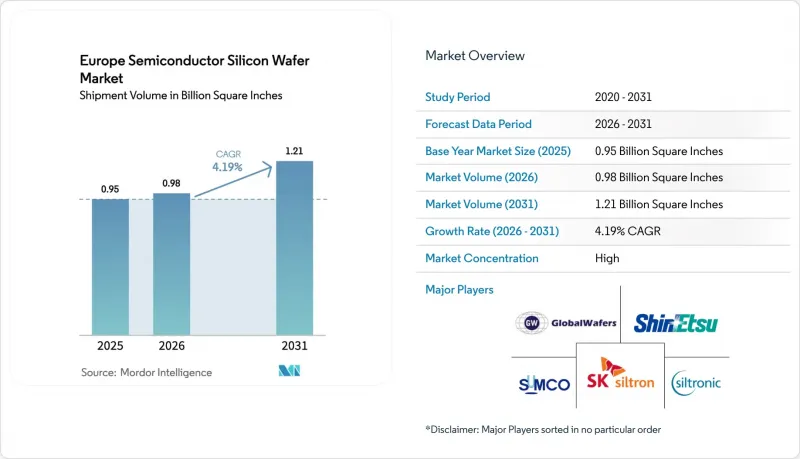
歐洲半導體矽晶圓市場(以出貨量為準)預計將從 2025 年的 9.5 億平方英寸和 2026 年的 9.8 億平方英寸成長到 2031 年的 12.1 億平方英寸,2026 年至 2031 年的年複合成長率(CAGR)為 4.19%。
在歐盟晶片法案的獎勵推動下,晶圓代工廠的擴張正在改變區域供應結構,但亞洲在通用基板市場仍然佔據主導地位,這為專注於高價值細分市場的歐洲供應商留下了發展空間。汽車電氣化和邊緣人工智慧的普及正在推動市場需求轉向300毫米優質拋光晶圓和絕緣體上矽(SOI)晶圓。功率元件向200毫米碳化矽晶圓的轉變維持了並行的需求流,在不阻礙300毫米晶圓成長的前提下,擴大了面向供應商的供應量。儘管競爭格局有利於資金雄厚的成熟企業,但擁有基板工程基板知識的專家正在獲得對5G、6G和量子運算藍圖至關重要的設計訂單。
歐洲半導體矽晶圓市場的趨勢與洞察
歐洲晶圓代工廠擴大300毫米晶圓產能
一座全新的300毫米待開發區工廠正在重塑歐洲半導體矽晶圓市場的成本模式。 GlobalWafers於2025年10月在義大利運作了其首個300毫米晶圓製造地。該基地年名目產能為100萬片晶圓,其中超過60%的產能已透過與意法半導體(STMicroelectronics)和英飛凌(Infineon)的長期合約得到保障。位於德勒斯登的合資企業「歐洲半導體製造公司」(European Semiconductor Manufacturing Company)將於2027年下半年開始試生產,每月額外供應4萬片晶圓,以滿足該地區對汽車節點基板的需求。 Siltronic位於新加坡的工廠擴建工程已於2024年完工,該工程也將把部分300毫米晶圓產能分配給面臨產能分配限制的歐洲買家。這些項目加在一起,將提升該地區在多晶矽價格方面的議價能力,並縮短汽車和工業領域關鍵生產環節的物流週期。
電動車和可再生能源電網對電力電子產品的需求不斷成長
在電氣化目標的驅動下,晶圓製造正朝著採用矽和碳化矽製造的高壓元件方向發展。英飛凌於2025年第一季在維拉赫啟動了200毫米碳化矽製程的生產,這將使牽引逆變器的生產成為可能,這些逆變器必須能夠承受超過1200V的電壓。義法半導體在第四季於卡塔尼亞採取了類似的舉措,而安森美半導體則決定在捷克共和國投資高達20億美元,建立端到端的碳化矽生產能力。歐盟支持的「轉型計畫」(Transform)及相關計畫正在建構一條歐洲碳化矽價值鏈,以減少對亞洲矽錠供應商的依賴。此外,電網級太陽能逆變器和採用高功率模組的風力發電機也帶來了需求,進一步擴大了基板的應用範圍。
歐洲供不應求
儘管瓦克化學公司於2025年7月擴建的蝕刻生產線已使歐洲半導體級多晶矽產量提升超過50%,但歐洲仍需從亞洲進口超過70%的原料。這種對外部資源的過度依賴使晶圓製造商面臨地緣政治衝擊和價格上漲的風險。 「轉型」計畫下建構一體化碳化矽供應鏈的努力凸顯了限制上游工程多元化的巨大資本和環境授權障礙。在新增精煉產能投入運作或達成具有約束力的長期採購協議之前,原物料短缺可能會抑制歐洲晶圓出貨量的成長。
細分市場分析
到2025年,300毫米晶圓節點將佔出貨量的73.61%,鞏固其作為邏輯和記憶體製程領先規格的地位,並主導歐洲晶圓廠的發展路線圖。隨著GlobalWafers位於諾瓦拉的工廠運作以及ESMC位於德勒斯登的工廠計劃擴產,300毫米晶圓的總合能將增加超過150萬片,進一步擴大歐洲半導體矽晶圓市場,尤其是拋光基板。 300毫米晶圓節點憑藉其單晶片成本優勢、與EUV光刻技術的兼容性以及與汽車級製程的緊密整合,保持著較高的運轉率利用率。
同時,受碳化矽 (SiC) 功率元件和專為汽車電氣化最佳化的類比產品的推動,對 200 毫米晶圓的需求持續成長。英飛凌菲拉赫工廠和意法半導體卡塔尼亞工廠的製程改造表明,就晶體生長特性和缺陷容差而言,200 毫米晶圓仍然適用於碳化矽晶圓。因此,歐洲半導體矽晶圓市場保持雙軌制結構:300 毫米晶圓推動產量成長,200 毫米晶圓確保穩定的利潤率,而 150 毫米以下的生產線則繼續專注於微機電系統 (MEMS) 和光電子等細分市場,這些市場主要由 Okmetic 的感測器級產品供應。
到2025年,邏輯晶圓將佔總產量的32.74%,這主要得益於邊緣人工智慧加速器和汽車微控制器對28nm-65nm製程節點的需求。歐洲晶圓廠正在大規模部署這些製程。台積電、博世、英飛凌和恩智浦在德勒斯登成立的合資企業正專注於這些微結構,預計這將推動邏輯晶圓在歐洲半導體矽晶圓市場的佔有率在預測期內持續成長。
由於歐洲通用DRAM產能有限,記憶體市佔率較小,但與FD-SOI專案相關的嵌入式非揮發性記憶體正在推動其細分市場的成長。類比和混合訊號元件的需求主要來自工業自動化和感測器介面,而高壓碳化矽分立元件則是歐洲半導體矽晶圓市場成長最快的領域,這主要得益於功率元件製造商外延晶圓訂單的激增。
《歐洲半導體矽晶圓市場報告》依晶圓直徑(150毫米以下、200毫米、300毫米)、半導體裝置類型(邏輯元件、記憶體、類比元件、分立元件、光電子元件、感測器、微元件)、晶圓類型(拋光面、外延面、SOI、特種細分、SOI、市場預測是基於出貨量(平方英吋)。
其他好處:
- Excel格式的市場預測(ME)表
- 3個月的分析師支持
目錄
第1章:引言
- 市場分析與定義的前提條件
- 分析範圍
第2章 分析方法
第3章執行摘要
第4章 市場狀況
- 市場概覽
- 產業價值鏈分析
- 市場促進因素
- 歐洲晶圓代工廠擴大300毫米晶圓產能
- 電動車和可再生能源電網對電力電子產品的需求不斷成長。
- 歐盟晶片法對國內半導體製造業的獎勵
- 在射頻和5G前端模組中採用SOI(絕緣體上矽)晶圓
- 邊緣人工智慧的引入正在推動 200 毫米邏輯和模擬節點的復興。
- 新型高電阻晶片:用於量子運算研發
- 市場限制因素
- 歐盟內部對多晶矽原料供應的限制
- 資本密集度高和投資回收期長會抑制新進者。
- 對亞洲晶圓加工設備的地緣政治依賴
- 由於環境法規,使用超純水的成本增加。
- 監理情勢
- 技術展望
- 宏觀經濟因素的影響
- 波特五力分析
- 供應商議價能力
- 買方的議價能力
- 新參與企業的威脅
- 替代品的威脅
- 競爭公司之間的競爭關係
第5章:市場規模與成長率預測(區域出貨量)
- 依晶圓直徑
- 最大可達 150 毫米
- 200 mm
- 300 mm
- 以半導體裝置類型分類
- 邏輯
- 記憶
- 模擬
- 離散的
- 光電子學
- 感應器
- 微控制器(MCU、MPU、DSP)
- 依晶片類型
- 拋光
- 外延
- 絕緣體上矽(SOI)
- 特種矽(高電阻、高功率、感測器級)
- 最終用戶
- 家用電子電器
- 行動裝置和智慧型手機
- 個人電腦和伺服器
- 工業的
- 溝通
- 車
- 其他終端用戶應用程式
- 家用電子電器
- 國家
- 德國
- 法國
- 英國
- 義大利
- 西班牙
- 俄羅斯
- 其他歐洲地區
第6章 競爭情勢
- 市場集中度
- 策略趨勢
- 市佔率分析
- 公司簡介
- Shin-Etsu Chemical Co., Ltd.
- SUMCO Corporation
- GlobalWafers Co., Ltd.
- Siltronic AG
- SK siltron Co., Ltd.
- SOITEC SA
- Okmetic Oy
- Wafer Works Corporation
- LG Siltron
- Shanghai Simgui Technology Co., Ltd.
- Topsil Semiconductor Materials A/S
- MEMC Electronic Materials, Inc.(GlobalFoundries)
- LOGOS Wafer Manufacturing
- Air Liquide Electronics
- NSIG Group
- Advanced Silicon SA
- Sumitomo Mitsubishi Silicon Corporation(SMS)
第7章 市場機會與未來展望
The Europe semiconductor silicon wafer market size in terms of shipment volume is projected to expand from 0.95 Billion Square Inches in 2025 and 0.98 Billion Square Inches in 2026 to 1.21 Billion Square Inches by 2031, registering a CAGR of 4.19% between 2026 to 2031.
Foundry expansions backed by EU Chips Act incentives are reshaping regional supply, yet Asia continues to dominate commodity substrates, leaving room for European suppliers focused on higher-value-add niches. Automotive electrification and edge-AI adoption are tilting demand toward 300-mm prime-polished and silicon-on-insulator wafers. Power-device migration to 200 mm silicon carbide formats is sustaining a parallel-diameter stream that widens the supplier's addressable volume without cannibalizing 300 mm growth. Competitive dynamics favor incumbents with capital depth, but specialty players that master engineered substrates are capturing design wins vital to 5G, 6G, and quantum computing roadmaps.
Europe Semiconductor Silicon Wafer Market Trends and Insights
Proliferation of 300 mm Wafer Capacity in European Foundries
New 300 mm greenfield plants are reshaping cost curves for the Europe semiconductor silicon wafer market. GlobalWafers brought Italy's first 300 mm site online in October 2025, with a nameplate output of 1 million wafers per year, of which more than 60% is secured under long-term contracts with STMicroelectronics and Infineon. The European Semiconductor Manufacturing Company joint venture in Dresden will draw an extra 40,000 wafers each month when pilot runs start in late 2027, anchoring regional substrate pull for automotive nodes. Siltronic's Singapore ramp, completed in 2024, also allocates part of its 300 mm output to European buyers facing capacity rationing. Together, these projects lift regional bargaining power on polysilicon pricing and shorten logistics loops for critical automotive and industrial volumes.
Growing Demand for Power Electronics in EV and Renewable Grid
Electrification targets are steering wafer mix toward high-voltage devices fabricated on both silicon and silicon carbide. Infineon began 200 mm SiC processing in Villach during the first quarter of 2025, enabling traction inverters that must handle voltages above 1,200 V. STMicroelectronics mirrored that move at Catania in the fourth quarter, and onsemi committed up to USD 2 billion for end-to-end SiC capacity in the Czech Republic. EU-backed Transform and related programs are knitting together a European SiC value chain that reduces reliance on Asian ingot suppliers. Demand also comes from grid-scale solar inverters and wind turbines that use ruggedized power modules, thereby driving broader substrate uptake.
Limited Polysilicon Feedstock Supply within Europe
Wacker Chemie's July 2025 etching-line expansion lifted regional semiconductor-grade polysilicon output by more than 50% but Europe still imports over 70% of feedstock from Asia. Heavy reliance on external sources exposes wafer makers to geopolitical shocks and price spikes. Building an integrated silicon carbide supply under the Transform program shows the scale of capital and environmental permitting hurdles that constrain upstream diversification. Until additional purification capacity comes online or binding long-term offtake deals are signed, feedstock tightness will cap upside for European wafer shipments.
Other drivers and restraints analyzed in the detailed report include:
- EU Chips Act Incentives for Domestic Semiconductor Manufacturing
- Adoption of Silicon-On-Insulator Wafers for RF and 5G Front-End Modules
- High Capital Intensity and Long ROI Deterring New Entrants
For complete list of drivers and restraints, kindly check the Table Of Contents.
Segment Analysis
The 300 mm node delivered 73.61% of shipments in 2025, confirming its position as the workhorse format for logic and memory processes that dominate European fab roadmaps. GlobalWafers' Novara launch and the forthcoming ESMC Dresden ramp collectively add more than 1.5 million wafers to the annual 300 mm capacity, deepening the Europe semiconductor silicon wafer market for prime-polished substrates. Cost-per-die advantages, compatibility with EUV lithography, and tight coupling to automotive-qualified process flows keep 300 mm utilisation high.
Parallel demand for 200 mm persists, propelled by silicon carbide power devices and analog products tailored to automotive electrification. Infineon's Villach and STMicroelectronics' Catania conversions prove that crystal-growth realities and defect budgets still favor 200 mm for SiC wafers. Consequently, the Europe semiconductor silicon wafer market retains a dual-diameter structure where 300 mm drives volume and 200 mm secures margin resilience, while up to 150 mm lines remain focused on MEMS and optoelectronic niches served by Okmetic's sensor-grade output.
Logic wafers represented 32.74% of 2025 volume, benefiting from edge-AI accelerators and automotive microcontrollers that rely on 28 nm-65 nm nodes, processes that European fabs are adding at scale. The Dresden joint venture between TSMC, Bosch, Infineon, and NXP focuses on precisely those geometries, which should widen the Europe semiconductor silicon wafer market size allocated to logic over the forecast horizon.
Memory holds a smaller slice due to Europe's limited commodity DRAM output, yet embedded non-volatile memory tied to FD-SOI projects keeps niche growth alive. Analog and mixed-signal devices ride industrial automation and sensor interface demand, while silicon carbide discretes for high-voltage drives are the fastest climber in the Europe semiconductor silicon wafer market, spurring a wave of epitaxial wafer orders from power-device manufacturers.
The Europe Semiconductor Silicon Wafer Market Report is Segmented by Wafer Diameter (Up To 150 Mm, 200 Mm, 300 Mm), Semiconductor Device Type (Logic, Memory, Analog, Discrete, Optoelectronics, Sensors, Micro), Wafer Type (Prime Polished, Epitaxial, Silicon-On-Insulator, Specialty Silicon), End-User (Telecommunications, and More), and Country. The Market Forecasts are Provided in Terms of Shipments by Volume (Square Inches).
List of Companies Covered in this Report:
- Shin-Etsu Chemical Co., Ltd.
- SUMCO Corporation
- GlobalWafers Co., Ltd.
- Siltronic AG
- SK siltron Co., Ltd.
- SOITEC S.A.
- Okmetic Oy
- Wafer Works Corporation
- LG Siltron
- Shanghai Simgui Technology Co., Ltd.
- Topsil Semiconductor Materials A/S
- MEMC Electronic Materials, Inc. (GlobalFoundries)
- LOGOS Wafer Manufacturing
- Air Liquide Electronics
- NSIG Group
- Advanced Silicon S.A.
- Sumitomo Mitsubishi Silicon Corporation (SMS)
Additional Benefits:
- The market estimate (ME) sheet in Excel format
- 3 months of analyst support
TABLE OF CONTENTS
1 INTRODUCTION
- 1.1 Study Assumptions and Market Definition
- 1.2 Scope of the Study
2 RESEARCH METHODOLOGY
3 EXECUTIVE SUMMARY
4 MARKET LANDSCAPE
- 4.1 Market Overview
- 4.2 Industry Value-Chain Analysis
- 4.3 Market Drivers
- 4.3.1 Proliferation of 300 mm Wafer Capacity in European Foundries
- 4.3.2 Growing Demand for Power Electronics in EV and Renewable Grid
- 4.3.3 EU Chips Act Incentives for Domestic Semiconductor Manufacturing
- 4.3.4 Adoption of Silicon-on-Insulator Wafers for RF and 5G Front-End Modules
- 4.3.5 Edge AI Adoption Driving 200 mm Logic and Analog Node Revivals
- 4.3.6 Emerging High-Resistivity Wafers for Quantum Computing R&D
- 4.4 Market Restraints
- 4.4.1 Limited Polysilicon Feedstock Supply within Europe
- 4.4.2 High Capital Intensity and Long ROI Deterring New Entrants
- 4.4.3 Geopolitical Dependency on Asia for Wafer Processing Equipment
- 4.4.4 Environmental Regulations Increasing Cost of Ultrapure Water Usage
- 4.5 Regulatory Landscape
- 4.6 Technological Outlook
- 4.7 Impact of Macroeconomic Factors
- 4.8 Porter's Five Forces Analysis
- 4.8.1 Bargaining Power of Suppliers
- 4.8.2 Bargaining Power of Buyers
- 4.8.3 Threat of New Entrants
- 4.8.4 Threat of Substitutes
- 4.8.5 Intensity of Competitive Rivalry
5 MARKET SIZE AND GROWTH FORECASTS (SHIPMENT IN AREA)
- 5.1 By Wafer Diameter
- 5.1.1 Up to 150 mm
- 5.1.2 200 mm
- 5.1.3 300 mm
- 5.2 By Semiconductor Device Type
- 5.2.1 Logic
- 5.2.2 Memory
- 5.2.3 Analog
- 5.2.4 Discrete
- 5.2.5 Optoelectronics
- 5.2.6 Sensors
- 5.2.7 Micro (MCU, MPU, DSP)
- 5.3 By Wafer Type
- 5.3.1 Prime Polished
- 5.3.2 Epitaxial
- 5.3.3 Silicon-on-Insulator (SOI)
- 5.3.4 Specialty Silicon (High-Resistivity, Power, Sensor-Grade)
- 5.4 By End-User
- 5.4.1 Consumer Electronics
- 5.4.1.1 Mobile and Smartphones
- 5.4.1.2 PCs and Servers
- 5.4.2 Industrial
- 5.4.3 Telecommunications
- 5.4.4 Automotive
- 5.4.5 Other End-User Applications
- 5.4.1 Consumer Electronics
- 5.5 By Country
- 5.5.1 Germany
- 5.5.2 France
- 5.5.3 United Kingdom
- 5.5.4 Italy
- 5.5.5 Spain
- 5.5.6 Russia
- 5.5.7 Rest of Europe
6 COMPETITIVE LANDSCAPE
- 6.1 Market Concentration
- 6.2 Strategic Moves
- 6.3 Market Share Analysis
- 6.4 Company Profiles (includes Global Level Overview, Market Level Overview, Core Segments, Financials as available, Strategic Information, Market Rank/Share, Products and Services, Recent Developments)
- 6.4.1 Shin-Etsu Chemical Co., Ltd.
- 6.4.2 SUMCO Corporation
- 6.4.3 GlobalWafers Co., Ltd.
- 6.4.4 Siltronic AG
- 6.4.5 SK siltron Co., Ltd.
- 6.4.6 SOITEC S.A.
- 6.4.7 Okmetic Oy
- 6.4.8 Wafer Works Corporation
- 6.4.9 LG Siltron
- 6.4.10 Shanghai Simgui Technology Co., Ltd.
- 6.4.11 Topsil Semiconductor Materials A/S
- 6.4.12 MEMC Electronic Materials, Inc. (GlobalFoundries)
- 6.4.13 LOGOS Wafer Manufacturing
- 6.4.14 Air Liquide Electronics
- 6.4.15 NSIG Group
- 6.4.16 Advanced Silicon S.A.
- 6.4.17 Sumitomo Mitsubishi Silicon Corporation (SMS)
7 MARKET OPPORTUNITIES AND FUTURE OUTLOOK
- 7.1 White-Space and Unmet-Need Assessment
 矽晶圓市場-全球產業規模、佔有率、趨勢、機會和預測:按晶圓尺寸、類型、應用、最終用戶、地區和競爭格局分類,2021-2031年
 300mm矽晶圓:市場佔有率分析、產業趨勢與統計、成長預測(2026-2031年)北美半導體矽晶圓:市場佔有率分析、產業趨勢與統計及成長預測(2026-2031 年)美國半導體矽晶圓:市場佔有率分析、行業趨勢和統計數據以及成長預測(2026-2031 年)
 矽晶圓市場規模、佔有率、趨勢和預測:按晶圓尺寸、類型、應用、最終用途和地區分類,2026-2034 年
 半導體矽晶圓回收市場:依回收製程、晶圓類型、晶圓尺寸、應用領域、產業及最終用戶分類-2026-2032年全球市場預測
 2026-2034年全球太陽能矽晶圓市場規模、佔有率、趨勢和成長分析報告5G半導體矽晶圓:市場佔有率分析、產業趨勢與統計及成長預測(2026-2031年)工業半導體矽晶圓:市場佔有率分析、產業趨勢與統計、成長預測(2026-2031)用於功率元件的矽晶圓:市場佔有率分析、行業趨勢和統計數據以及成長預測(2026-2031 年)