


 |
市場調查報告書
商品編碼
2099762
HBM在網路交換和封包處理中的應用:市場佔有率分析、行業趨勢和統計數據以及成長預測(2026-2031)HBM For Network Switching and Packet Processing - Market Share Analysis, Industry Trends & Statistics, Growth Forecasts (2026 - 2031) |
||||||

※ 本網頁內容可能與最新版本有所差異。詳細情況請與我們聯繫。
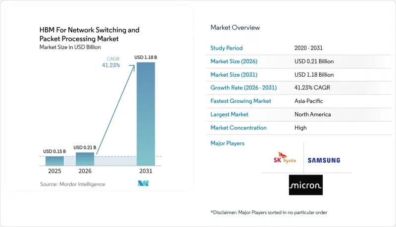
據 Mordor Intelligence 稱,用於網路交換和封包處理的 HBM 市場預計將從 2025 年的 1.5 億美元成長到 2026 年的 2.1 億美元,到 2031 年達到 11.8 億美元,2026 年至 2031 年的複合年成長率為 41.23%。
本報告按應用領域(乙太網路切換器ASIC、資料處理單元、智慧網卡等)、HBM代數(HBM3E、HBM4等)、單堆疊記憶體容量(16 GB、24 GB等)、終端用戶產業(雲端資料中心、企業網路等)和地區(北美、亞太等)進行細分。市場預測以美元計價。
網路交換和封包處理中的 HBM 全球趨勢和見解
AI最佳化型交換器ASIC和封包緩衝區的頻寬需求不斷成長
隨著人工智慧訓練叢集規模超過 10 萬個加速器,網路交換和封包處理領域的 HBM 市場發展受到記憶體頻寬明顯限制的驅動,而傳統的片上 SRAM 無法單獨滿足這一需求。一篇發表於 2026 年 1 月的 IEEE 論文指出,與無交換器 HBM 配置相比,HBM-NS 架構的能耗降低了 32.1%,延遲降低了 55%,這證明了近記憶體交換作為實用的網路設計方案的有效性。另一篇發表於 2026 年 NSDI 會議的論文指出,基於 HBM 的混合緩衝區管理在 400 Gbps 連接埠速率下可將端到端網路效能提升高達 2.8 倍,這表明 HBM 網路交換和封包處理市場擁有強大的效能基礎,而不僅僅體現在頻寬方面。此外,隨著網路從400G邁向800G,再到1.6T,大規模AI叢集面臨著持續時間更長的擁塞和更高密度的流量突發,導致負載迅速增加,而這僅靠連接埠速度的提升無法解釋。這一趨勢推動了對更大容量緩衝區池的需求,高容量HBM配置在整個HBM市場(用於網路交換和封包處理)中也變得越來越普遍。
在Terabit特級網路交換平台中採用共封裝HBM
用於網路交換和封包處理的 HBM 市場於 2024 年 3 月迎來了其首個封裝藍圖。當時,博通公司發布了全球首款 51.2 Tbps 共封裝光乙太網路切換器平台,將 HBM、矽光電和交換邏輯整合於單一封裝中。 2025 年 10 月,博通公司推出了 102.4 Tbps 的 Tomahawk 6 Davisson,進一步擴展了這個模式,在保持 HBM 為系統結構核心的同時,將頻寬提升至先前共封裝交換器設計的兩倍。 2026 年 6 月,Marvell 公司發布了 102.4 Tbps 的 Teralynx T100,為 AI 和雲端資料中心網路提供了多種封裝選擇,進一步強化了這個發展方向。這種共封裝方式正在改變網路交換和封包處理市場中 HBM 的採購模式,因為超大規模資料中心業者大規模資料中心越來越重視將 HBM 和 ASIC 整合到一起的封裝,而不是單獨評估記憶體和交換組件。因此,能夠及早調整其記憶體藍圖、封裝通路和晶片切換計畫的供應商,在搶佔大規模引進週期處於有利地位。
HBM整合大規模生產缺乏先進的封裝能力
用於網路交換和封包處理的 HBM 市場仍然嚴重依賴先進封裝的生產能力,尤其是在將 HBM 和交換邏輯整合到單一封裝中的設計方面,產能的緊張程度遠遠超過了終端用戶的需求。博通最新的 Tomahawk 和 Jericho 平台,以及 Marvell 的 Teralynx T100,都展現出依賴先進封裝而非獨立記憶體連接的設計方向。這使得網路晶片和 AI 加速器之間在封裝資源方面進入許可權直接競爭,從而使最大的買家和早期進入者在網路交換和封包處理HBM 市場中擁有明顯的優勢。因此,即使擁有可靠的技術藍圖和客戶需求,規模小規模的網路供應商在擴展規模方面也面臨更大的挑戰。最終導致供應環境兩極化:頂級超超大規模資料中心業者可以快速擴張,而二級 OEM 和企業級供應商則難以進入量產階段。
細分市場分析
2025年,乙太網路切換器ASIC在網路交換和封包處理領域佔據了43.13%的HBM市場佔有率,但預計2026年至2031年間,AI網路架構交換器的複合年成長率將達到42.03%。這項銷售領先優勢反映了其在超大規模葉脊式乙太網路環境中的長期部署,在這些環境中,深度緩衝交換已成為處理大規模東西向流量的實際需求。據博通公司稱,Jericho4的包緩衝區容量是標準片上內存的160倍,這解釋了為什麼深度緩衝以太網平台在2025年和2026年仍然是高性能AI網路設計的核心。同時,用於網路交換和封包處理的HBM市場正在向客製化AI架構轉型。此外,NVIDIA和Marvell於2026年3月達成合作,並獲得了20億美元的投資,這將使高級資料包管理和可擴展網路與支援HBM的設計更加緊密地結合起來。
下一個需求層正從更靠近伺服器、網路邊緣或通訊控制平面的介面和封包處理設備中湧現。根據博通的 BCM88690 資料手冊,網路處理硬體已經採用了雙 HBM Gen2 立方體,總合擁有 8 GB 的資料包緩衝區,並支援多達 128,000 個可程式設計隊列,這意味著即使在規模最大的 AI 架構之外,NPU 仍然在確定性流量處理中發揮著至關重要的作用。這對 HBM 在網路交換和封包處理行業中具有重大意義,因為它表明該技術不僅限於頂級交換器 ASIC,還可以處理佇列負載高、延遲敏感的封包處理工作負載。隨著記憶體良率的提高、每位元成本的降低以及基於 HBM 的流量管理在更多網路功能中更容易得到應用,預計應用需求將從最高效能的交換層進一步擴展到相鄰裝置。
預計到2025年,HBM3將佔據55.92%的市場佔有率,成為HBM系列產品中網路交換封包處理市場佔有率最大的晶片。同時,HBM4預計將以42.21%的複合年成長率成長至2031年。 HBM3的領先優勢主要得益於博通StrataDNX Jericho系列和Tomahawk系列系統在2024年至2025年間投入量產,這為該系列晶片在已部署的交換平台中奠定了最堅實的商業性基礎。 HBM2和HBM2E仍應用於傳統的深緩衝平台,但隨著網路朝向400G及以上交換速度發展,它們的單引腳頻寬已不再適用。根據博通BCM88480的文檔,早期HBM Gen2設計仍然應用於現有路由器系統中,其封裝內包含4GB的緩衝內存,這也解釋了為什麼儘管新一代晶片市場佔有率不斷成長,老一代晶片並沒有立即被淘汰。
用於網路交換和封包處理的HBM市場目前正向HBM3E和HBM4轉型。這是因為下一代交換晶片需要更寬的介面和更高的頻寬。以色列理工學院、加州大學柏克萊分校和加州大學聖地牙哥分校的研究表明,採用四個HBM4堆疊的「封裝路由器」設計可以實現81.92 Tbps的總合交換頻寬,凸顯了下一代記憶體架構的潛力。三星於2026年2月開始量產HBM4,英偉達和SK海力士於2026年6月正式簽署了一項多年技術合作協議,旨在推進用於人工智慧工廠的下一代記憶體的開發。這兩項進展都明確了未來供應鏈的前景。這些舉措支持了這樣一種觀點:隨著下一代交換技術實現量產,用於網路交換和封包處理的HBM市場將繼續向更寬頻寬的2048位元介面和更高的單棧頻寬。
區域分析
2025年,北美在用於網路交換和封包處理的HBM市場中佔據44.68%的佔有率。這一領先地位源自於美國是超大規模先進交換晶片的最大買家,也是首個大規模採用高階HBM網路平台的地區。 2026年,Google宣布其Virgo網路將採用扁平化、無阻塞設計,連接13.4萬個TPU晶片,實現高達47PB/s的二分頻寬。這反映了北美通訊業者已規劃和部署的基礎設施規模。此類部署需要比傳統設計具有更高記憶體頻寬和資料包緩衝能力的交換器。因此,用於網路交換和封包處理的HBM市場與該地區的超大規模投資週期密切相關。此外,政府需求也支撐了該地區的市場基礎,例如美國國家核安全管理局(NNSA)支持Cornelis Networks為其國家運算計畫開發下一代網路。
到2025年,歐洲也將佔據相當大的佔有率,德國、英國、法國和北歐國家將部署大規模雲園區和高容量網路。該地區也受惠於5G獨立組網核心網的升級,這進一步激發了人們對配備更先進記憶體子系統的分組處理器和路由系統的持續興趣。英國和德國的國家人工智慧計畫正在推動未來資料中心的持續投資,預計這將推動先進交換半導體在預測期內的逐步普及。歐洲也具有降低對半導體和封裝能力長期依賴的戰略利益。儘管如此,台灣仍然是網路交換封包處理市場中HBM封裝的領先中心。
預計到2031年,亞太地區將以42.23%的複合年成長率成長,成為網路交換和封包處理領域HBM市場成長最快的地區。韓國是供應鏈的核心,這得益於SK海力士在2025年創下的業績紀錄,以及英偉達於2026年6月與SK海力士就用於人工智慧基礎設施的下一代內存達成的多年技術合作協議。台灣仍然至關重要,因為博通和Marvell的尖端人工智慧交換平台依賴與台灣半導體生態系統深度融合的封裝密集型組裝流程。雖然印度和東南亞的HBM應用仍處於早期階段,但國內雲端投資正開始創造對整合HBM交換平台的未來需求。南美、中東和非洲仍然代表著長期機遇,在這些地區,企業現代化和政府網路升級是主要的短期促進因素,而非大規模人工智慧架構部署。
其他好處:
- Excel格式的市場預測(ME)表
- 3個月的分析師支持
目錄
第1章:引言
- 研究假設和市場定義
- 調查範圍
第2章:調查方法
第3章執行摘要
第4章 市場狀況
- 市場概覽
- 市場促進因素
- AI最佳化型交換器ASIC和封包緩衝區的頻寬需求不斷成長
- 在Terabit特級網路交換平台中採用共封裝HBM
- 向超大規模資料中心的記憶體回彈網路架構過渡
- 800G 和 1.6T 乙太網路的引入提高了對緩衝區深度和延遲的敏感度。
- 透過與電腦類似的記憶體整合,提高了散熱和電源效率。
- 用於通訊設備中確定性封包處理的富含 HBM 的邊緣網路
- 市場限制因素
- HBM整合中缺乏先進的封裝生產能力,無法實現大規模生產
- 先進DRAM節點的出口限制與認證限制
- 在具有大量堆疊的 HBM 架構中,良率風險急劇增加。
- 與客製化ASIC藍圖的緊密協調正在減緩網路技術的廣泛應用。
- 產業價值鏈分析
- 宏觀經濟因素對市場的影響
- 監理情勢
- 技術展望
- 波特五力分析
第5章 市場規模與成長預測
- 透過使用
- 乙太網路切換器專用積體電路 (ASIC)
- 資料處理單元(DPU)
- SmartNICs
- 網路處理單元(NPU)
- AI網路架構交換器
- 按世代分類的 HBM
- HBM2
- HBM2E
- HBM3
- HBM3E
- HBM4
- 每個堆疊的記憶體容量
- 4 GB
- 8 GB
- 16 GB
- 24 GB
- 32 GB 或更多
- 按最終用戶行業分類
- 雲端資料中心
- 電訊
- 企業網路
- 政府/國防
- 高效能運算網路
- 按地區
- 北美洲
- 美國
- 加拿大
- 墨西哥
- 歐洲
- 德國
- 英國
- 法國
- 義大利
- 其他歐洲國家
- 亞太地區
- 中國
- 日本
- 韓國
- 台灣
- 印度
- 其他亞太國家
- 南美洲
- 中東和非洲
- 北美洲
第6章 競爭情勢
- 市場集中度
- 策略趨勢
- 市佔率分析
- 公司簡介
- SK hynix Inc.
- Samsung Electronics Co., Ltd.
- Micron Technology, Inc.
- 其他生態系公司
- NVIDIA Corporation
- Advanced Micro Devices, Inc.
- Intel Corporation
- Broadcom Inc.
- Marvell Technology, Inc.
- Taiwan Semiconductor Manufacturing Company Limited
- ASE Technology Holding Co., Ltd.
- Amkor Technology, Inc.
- Powertech Technology Inc.
- United Microelectronics Corporation
- Rambus Inc.
- Cadence Design Systems, Inc.
- Synopsys, Inc.
- Applied Materials, Inc.
- Qualcomm Incorporated
- Fujitsu Limited
- Texas Instruments Incorporated
第7章 市場機會與未來展望
According to Mordor Intelligence, the HBM for network switching and packet processing market is expected to increase from USD 0.15 billion in 2025 to USD 0.21 billion in 2026, and reach USD 1.18 billion by 2031, growing at a CAGR of 41.23% over 2026-2031.
This report is Segmented by Application (Ethernet Switch ASICs, Data Processing Units, Smartnics, and More), HBM Generation ( HBM3E, HBM4, and More), Memory Capacity Per Stack (16 GB, 24 GB, and More), End-User Industry (Cloud Data Centers, Enterprise Networking, and More), and Geography (North America, Asia-Pacific, and More). The Market Forecasts are Provided in Terms of Value (USD).
Global HBM For Network Switching and Packet Processing Market Trends and Insights
Rising AI-Optimized Switch ASIC and Packet-Buffer Bandwidth Requirements
As AI training clusters moved past 100,000 accelerators, the HBM market for network switching and packet processing was pushed by a clear memory bandwidth limit that conventional on-die SRAM could not address on its own. A January 2026 IEEE paper on the HBM-NS architecture reported 32.1% lower energy use and 55% lower latency than switchless HBM configurations, supporting the case for near-memory switching as a practical network design option. The Themis paper presented at NSDI 2026 found that HBM-based hybrid buffer management improved end-to-end network performance by up to 2.8 times at 400 Gbps port speeds, providing a strong performance case for the HBM network-switching and packet-processing market beyond simple bandwidth claims. The pressure also rises faster than port speed alone suggests, because larger AI clusters create longer congestion events and denser traffic bursts as networks move from 400G to 800G and then toward 1.6T. That pattern is increasing demand for deeper buffer pools and helping higher-capacity HBM configurations gain ground across the HBM market for network switching and packet processing.
Co-Packaged HBM Adoption in Terabit-Class Network Switching Platforms
The HBM for network switching and packet processing market gained an early packaging blueprint when Broadcom introduced the first 51.2 Tbps co-packaged optics Ethernet switch platform in March 2024 with HBM, silicon photonics, and switch logic assembled in one package. Broadcom extended that model in October 2025 with the Tomahawk 6 Davisson at 102.4 Tbps, which doubled the bandwidth of earlier co-packaged switch designs while keeping HBM at the center of the system architecture. Marvell reinforced this direction in June 2026, when it launched the 102.4 Tbps Teralynx T100 with multiple packaging options for AI and cloud data center networking. This co-packaged approach changes the buying unit within the HBM for the network switching and packet processing market, as hyperscalers increasingly evaluate a combined HBM-ASIC package rather than separate memory and switch components. Vendors that can align memory roadmaps, packaging access, and switch silicon schedules earlier are therefore in a better position to capture the largest deployment cycles.
Limited Advanced Packaging Capacity for High-Volume HBM Integration
The HBM market for network switching and packet processing still depends on advanced packaging capacity that remains tighter than end demand, especially for designs that place HBM and switching logic in a single package. Broadcom's latest Tomahawk and Jericho platforms, along with Marvell's Teralynx T100, all point to a design direction that relies on sophisticated packaging rather than stand-alone memory attachment. That creates direct competition for packaging access between networking silicon and AI accelerators, giving the largest buyers and earliest reservers an obvious advantage in the HBM for network switching and packet processing market. Smaller networking vendors, therefore, face a harder path to scale, even when their technical roadmaps are sound and customer demand is present. The result is a two-speed supply environment in which top hyperscalers can move faster, while second-tier OEMs and enterprise-oriented vendors face slower ramp timing.
Other drivers and restraints analyzed in the detailed report include:
- Hyperscale Data Center Migration Toward Memory-Bound Network Architectures
- 800G and 1.6T Ethernet Rollouts Increasing Buffer Depth and Latency Sensitivity
- Export Controls and Qualification Constraints on Advanced DRAM Nodes
For complete list of drivers and restraints, kindly check the Table Of Contents.
Segment Analysis
Ethernet switch ASICs held 43.13% of the HBM market share for network switching and packet processing in 2025, while AI networking fabric switches are projected to grow at a 42.03% CAGR from 2026 to 2031. That revenue lead reflected years of deployment in hyperscale leaf-spine Ethernet environments, where deep-buffer switching had already become a practical requirement for large east-west traffic loads. Broadcom said Jericho4 delivered 160 times the packet buffer capacity of standard on-chip memory, which explains why deep-buffer Ethernet platforms remained central to high-performance AI network design in 2025 and 2026. At the same time, the HBM for network switching and packet processing market is being pulled toward custom AI fabrics, and NVIDIA's March 2026 partnership with Marvell, backed by a USD 2 billion investment, has more tightly linked advanced packet management and scale-up networking to HBM-aware designs.
The next layer of demand comes from interface and packet-processing devices that sit closer to the server, the network edge, or the telecom control plane. Broadcom's BCM88690 datasheet showed that network processing hardware already used dual HBM Gen2 cubes for a total of 8 GB of packet buffer and supported up to 128,000 programmable queues, which kept NPUs relevant for deterministic traffic handling beyond the largest AI fabrics. That matters for the HBM in the network switching and packet processing industry because it shows that the technology is not limited to top-end switch ASICs and can also support queue-heavy, latency-sensitive packet processing workloads. Over time, application demand is likely to keep widening from the highest-performance switching tier into adjacent devices as memory yields improve, per-bit economics ease, and HBM-backed traffic management becomes easier to justify across more networking functions.
HBM3 commanded a 55.92% share in 2025, giving it the largest position in the HBM for network switching and packet processing market size by HBM generation, while HBM4 is projected to expand at a 42.21% CAGR through 2031. HBM3 built that lead because Broadcom's StrataDNX Jericho family and Tomahawk-class systems moved into production across 2024 and 2025, which gave this generation the strongest commercial footing in deployed switching platforms. HBM2 and HBM2E remained in legacy deep-buffer platforms, but their bandwidth-per-pin profile is becoming less suitable as networks move deeper into 400G-and-above switching. Broadcom's BCM88480 documentation illustrated that earlier HBM Gen2 designs still served installed router systems with 4 GB of in-package buffer memory, which shows why older generations did not disappear immediately, even as newer ones gained share.
The HBM market for network switching and packet processing is now moving toward HBM3E and HBM4, as next-generation switch silicon requires wider interfaces and greater bandwidth per stack. Research from Technion, UC Berkeley, and UC San Diego showed that a router-in-a-package design using 4 HBM4 stacks could deliver 81.92 Tbps of combined switching bandwidth, which highlighted the architectural headroom of the next memory generation. Samsung began HBM4 mass production in February 2026, and NVIDIA and SK Hynix formalized a multiyear technology partnership in June 2026 to advance next-generation memory for AI factories, both of which improved visibility around the future supply base. Those moves support the view that the HBM market for network switching and packet processing will continue shifting toward wider 2,048-bit interfaces and higher per-stack bandwidth as the next switching wave reaches production.
Complete Report Scope:
- By Application
- Ethernet Switch ASICs
- Data Processing Units (DPUs)
- SmartNICs
- Network Processing Units (NPUs)
- AI Networking Fabric Switches
- By HBM Generation
- HBM2
- HBM2E
- HBM3
- HBM3E
- HBM4
- By Memory Capacity Per Stack
- 4 GB
- 8 GB
- 16 GB
- 24 GB
- 32 GB and Above
- By End-User Industry
- Cloud Data Centers
- Telecommunications
- Enterprise Networking
- Government and Defense
- High-Performance Computing Networks
- By Geography
- North America
- United States
- Canada
- Mexico
- Europe
- Germany
- United Kingdom
- France
- Italy
- Rest of Europe
- Asia-Pacific
- China
- Japan
- South Korea
- Taiwan
- India
- Rest of Asia-Pacific
- South America
- Middle East and Africa
- North America
Geography Analysis
North America held 44.68% of the HBM for the network switching and packet processing market share in 2025. The region led because the United States was home to the largest hyperscale buyers of advanced switch silicon and was the first to adopt high-end HBM-backed networking platforms at scale. Google disclosed in 2026 that its Virgo network linked 134,000 TPU chips in a flat, non-blocking design and delivered up to 47 petabits per second of bisectional bandwidth, reflecting the scale of infrastructure that North American operators were already planning and deploying. That kind of deployment favors switches with far deeper memory bandwidth and packet buffering than conventional designs can provide, which keeps the HBM for network switching and packet processing market closely aligned with the region's hyperscale spending cycle. Government demand also supported the regional base after the NNSA backed next-generation networking work with Cornelis Networks for national computing programs.
Europe contributed a meaningful share in 2025, with Germany, the United Kingdom, France, and the Nordic countries hosting major cloud campuses and high-capacity network deployments. The region also benefited from 5G standalone core upgrades, which supported ongoing interest in packet processors and routing systems with richer memory subsystems. National AI programs in the United Kingdom and Germany are helping sustain future data center investment, which should support the gradual uptake of advanced switching silicon over the forecast period. Europe also has a strategic interest in reducing long-term dependence on semiconductor and packaging capabilities, even though Taiwan remains the central packaging hub for HBM in the network switching and packet processing market today.
Asia-Pacific is projected to grow at a 42.23% CAGR through 2031, making it the fastest-growing region in the HBM for network switching and packet processing market. South Korea sits at the center of supply because SK hynix posted record FY25 results, and NVIDIA entered a multiyear technology partnership with SK hynix in June 2026 for next-generation memory used in AI infrastructure. Taiwan remains indispensable because the most advanced AI-focused switch platforms from Broadcom and Marvell rely on package-intensive assembly paths that are deeply linked to the island's semiconductor ecosystem. India and Southeast Asia are earlier in adoption, but domestic cloud investment is beginning to create future demand for HBM-integrated switching platforms. South America,d the Middle East,t and Africa remain longer-horizon opportunities, where enterprise modernization and government network upgrades are more important near-term drivers than large AI fabric deployments.
- SK hynix Inc.
- Samsung Electronics Co., Ltd.
- Micron Technology, Inc.
Additional Benefits:
- The market estimate (ME) sheet in Excel format
- 3 months of analyst support
TABLE OF CONTENTS
1 INTRODUCTION
- 1.1 Study Assumptions and Market Definition
- 1.2 Scope of the Study
2 RESEARCH METHODOLOGY
3 EXECUTIVE SUMMARY
4 MARKET LANDSCAPE
- 4.1 Market Overview
- 4.2 Market Drivers
- 4.2.1 Rising AI-Optimized Switch ASIC and Packet-Buffer Bandwidth Requirements
- 4.2.2 Co-Packaged HBM Adoption in Terabit-Class Network Switching Platforms
- 4.2.3 Hyperscale Data Center Migration Toward Memory-Bound Network Architectures
- 4.2.4 800G and 1.6T Ethernet Rollouts Increasing Buffer Depth and Latency Sensitivity
- 4.2.5 Thermal and Power-Efficiency Gains From Near-Compute Memory Integration
- 4.2.6 HBM-Rich Edge Networking for Deterministic Packet Processing in Telecom Equipment
- 4.3 Market Restraints
- 4.3.1 Limited Advanced Packaging Capacity for High-Volume HBM Integration
- 4.3.2 Export Controls and Qualification Constraints on Advanced DRAM Nodes
- 4.3.3 Yield Risk Increases Rapidly With Higher-Stack HBM Architectures
- 4.3.4 Tight Coupling to Custom ASIC Roadmaps Slows Broader Networking Adoption
- 4.4 Industry Value Chain Analysis
- 4.5 Impact of Macroeconomic Factors on the Market
- 4.6 Regulatory Landscape
- 4.7 Technological Outlook
- 4.8 Porter's Five Forces Analysis
- 4.8.1 Bargaining Power of Suppliers
- 4.8.2 Bargaining Power of Buyers
- 4.8.3 Threat of New Entrants
- 4.8.4 Threat of Substitutes
- 4.8.5 Intensity of Competitive Rivalry
5 MARKET SIZE AND GROWTH FORECASTS (VALUE)
- 5.1 By Application
- 5.1.1 Ethernet Switch ASICs
- 5.1.2 Data Processing Units (DPUs)
- 5.1.3 SmartNICs
- 5.1.4 Network Processing Units (NPUs)
- 5.1.5 AI Networking Fabric Switches
- 5.2 By HBM Generation
- 5.2.1 HBM2
- 5.2.2 HBM2E
- 5.2.3 HBM3
- 5.2.4 HBM3E
- 5.2.5 HBM4
- 5.3 By Memory Capacity Per Stack
- 5.3.1 4 GB
- 5.3.2 8 GB
- 5.3.3 16 GB
- 5.3.4 24 GB
- 5.3.5 32 GB and Above
- 5.4 By End-User Industry
- 5.4.1 Cloud Data Centers
- 5.4.2 Telecommunications
- 5.4.3 Enterprise Networking
- 5.4.4 Government and Defense
- 5.4.5 High-Performance Computing Networks
- 5.5 By Geography
- 5.5.1 North America
- 5.5.1.1 United States
- 5.5.1.2 Canada
- 5.5.1.3 Mexico
- 5.5.2 Europe
- 5.5.2.1 Germany
- 5.5.2.2 United Kingdom
- 5.5.2.3 France
- 5.5.2.4 Italy
- 5.5.2.5 Rest of Europe
- 5.5.3 Asia-Pacific
- 5.5.3.1 China
- 5.5.3.2 Japan
- 5.5.3.3 South Korea
- 5.5.3.4 Taiwan
- 5.5.3.5 India
- 5.5.3.6 Rest of Asia-Pacific
- 5.5.4 South America
- 5.5.5 Middle East and Africa
- 5.5.1 North America
6 COMPETITIVE LANDSCAPE
- 6.1 Market Concentration
- 6.2 Strategic Moves
- 6.3 Market Share Analysis
- 6.4 Company Profiles (includes Global Level Overview, Market Level Overview, Core Segments, Financials as available, Strategic Information, Products and Services, Recent Developments)
- 6.4.1 SK hynix Inc.
- 6.4.2 Samsung Electronics Co., Ltd.
- 6.4.3 Micron Technology, Inc.
- 6.5 Other Ecosystem Players
- 6.5.1 NVIDIA Corporation
- 6.5.2 Advanced Micro Devices, Inc.
- 6.5.3 Intel Corporation
- 6.5.4 Broadcom Inc.
- 6.5.5 Marvell Technology, Inc.
- 6.5.6 Taiwan Semiconductor Manufacturing Company Limited
- 6.5.7 ASE Technology Holding Co., Ltd.
- 6.5.8 Amkor Technology, Inc.
- 6.5.9 Powertech Technology Inc.
- 6.5.10 United Microelectronics Corporation
- 6.5.11 Rambus Inc.
- 6.5.12 Cadence Design Systems, Inc.
- 6.5.13 Synopsys, Inc.
- 6.5.14 Applied Materials, Inc.
- 6.5.15 Qualcomm Incorporated
- 6.5.16 Fujitsu Limited
- 6.5.17 Texas Instruments Incorporated
7 MARKET OPPORTUNITIES AND FUTURE OUTLOOK
- 7.1 White-Space and Unmet-Need Assessment

 2026-2034年全球汽車人工智慧晶片組市場規模、佔有率、趨勢和成長分析報告全球人工智慧晶片組市場規模、佔有率、趨勢和成長分析報告(2026-2034)
 人工智慧晶片組:市場佔有率分析、產業趨勢與統計及成長預測(2026-2031 年)HBM在國防和航太運算領域的應用:市場佔有率分析、產業趨勢和統計數據以及成長預測(2026-2031年)
 人工智慧(AI)晶片組市場:2026-2032年全球市場預測(按晶片組類型、架構、部署方式、應用和最終用途分類)AI GPU晶片:市佔率分析、產業趨勢與統計及成長預測(2026-2031年)HBM在人工智慧推理中的應用:市場佔有率分析、行業趨勢與統計數據以及成長預測(2026-2031年)HBM在AI GPU的應用:市佔率分析、產業趨勢與統計、成長預測(2026-2031)
 人工智慧影像處理晶片市場:按晶片類型、部署模式、應用、終端用戶產業、國家和地區分類-產業分析、市場規模、市場佔有率及2026年至2033年預測GPU架構與運算IP授權:市場佔有率分析、產業趨勢與統計資料以及成長預測(2026-2031年)