

 |
市場調查報告書
商品編碼
2065435
GPU架構與運算IP授權:市場佔有率分析、產業趨勢與統計資料以及成長預測(2026-2031年)GPU Architecture And Compute IP Licensing - Market Share Analysis, Industry Trends & Statistics, Growth Forecasts (2026 - 2031) |
||||||
※ 本網頁內容可能與最新版本有所差異。詳細情況請與我們聯繫。
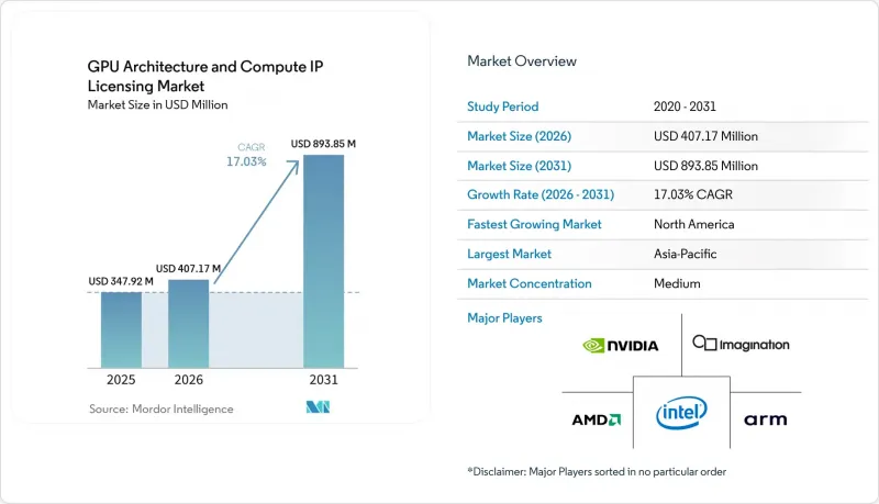
GPU架構與運算IP授權市場預計將從2025年的3.4792億美元成長到2026年的4.0717億美元,到2031年達到8.9385億美元,2026年至2031年的複合年成長率為17.03%。
本報告按IP類型(GPU核心IP、AI/張量計算IP、計算ISA/架構IP、片上計算互連IP)、許可模式(永久許可+版稅、訂閱/訪問許可等)、最終用戶(無晶圓半導體公司、整合設備製造商等)和地區進行細分。市場預測以美元(USD)為單位。
全球GPU架構與運算IP授權市場趨勢及洞察
資料中心人工智慧工作負載的爆炸性成長
超大規模雲端服務供應商正在獲得 TensorCore IP 的授權,以建立特定應用的加速器,從而降低每次推理的能耗成本,並避免使用獨立 GPU 帶來的利潤空間。 AWS 於 2025 年 3 月推出的 Trainium 2 實例,其每瓦效能比 H100叢集提升了 30%,每年可為營運商節省 12 億美元的 GPU 採購成本。谷歌與博通聯合開發的 TPU v6e,與同類 GPU 叢集相比,能耗成本降低了三分之一。英偉達與 Groq 達成的 200 億美元交易表明,即使是專注於推理的新創公司也在尋求 IP 的使用權,以保持藍圖的柔軟性。這種授權趨勢將加速收入成長,因為「永久授權 + 版稅」或訂閱模式允許超大規模資料中心業者每 18 個月更新一次系統,而無需重新談判供應合約。由此產生的需求成長將使整體複合年成長率 (CAGR) 預測值提高 5.2%。
邊緣人工智慧設備的普及
智慧型手機、消費性物聯網節點和智慧家庭設備需要滿足隱私要求且延遲低於 100 毫秒的設備內生成模型。高通驍龍 8 Elite 整合了 AI 張量切片,擁有 45 TOPS 的處理能力,可用於即時影片分割。聯發科天璣 9400 將 Arm Mali-G925 GPU IP 與 16 核心 NPU 結合,可在本地運行 70 億個參數模型。 Arm 預計,在 Mali 和 Immortalis 晶片出貨量達到 18 億顆的推動下,其 2025 會計年度的專利使用費收入將成長 34%。 IMG CXT 收購了三級 ADAS 插槽,進一步提振了汽車產業的需求。廣泛的設計應用預計將推動 3.8% 的複合年成長率。
先進節點的初始非重複性工程成本較高
3nm 和 2nm 製程的掩模組成本現已超過 3,000 萬美元,首片成本甚至可達 8,000 萬美元,這使得許多中型無廠半導體公司無緣採用尖端設計。 CoWoS 封裝成本已從 2023 年的每晶片 900 美元上漲至 1500 美元。三星的 3nm 環柵 (GAA) 製程節點成本降低了 15%,但其首批流片卻延遲了六個月。作為回應,小規模的授權公司正加速向成熟的 7nm 製程節點遷移並採用晶片組,但這犧牲了能源效率。這一投資壁壘導致預計的複合年成長率下降了 2.8%。
細分市場分析
預計到2025年,GPU核心IP將佔總收入的44%,這一地位主要得益於Arm Mali和Imagination PowerVR系列產品,這兩款產品每年應用於超過20億台設備。人工智慧和張量計算IP正以21.90%的複合年成長率快速成長,因為超超大規模資料中心業者優先考慮INT8和稀疏引擎而非光柵化引擎,並將支出轉向專用矩陣處理模組。 Nvidia與Groq的合作表明,授權商越來越關注Blackwell世代的張量核心和用於出口受限推理晶片的NVLink架構。計算指令集架構(ISA)IP(主要由RISC-V向量擴充組成)的市佔率已達18%,主要得益於歐洲和印度的獨立開發案尋求免版稅指令集。片上互連IP的市佔率已達14%,因為晶片組的普及催生了對延遲低於100奈秒的網狀互連的需求。
超大規模資料中心業者也傾向採用稀疏張量加速器,以提高每瓦運算效能,Google的 TPU v6e 就是一個例子。它透過整合客製化的稀疏邏輯,將密集矩陣處理吞吐量提高了 2.4 倍。 Meta 的 MTIA v2 僅授權其記憶體控制器和互連模組,同時自行設計推理單元。 SiFive 的 Intelligence X390 NPU 將 RISC-V 向量與 128 通道矩陣引擎融合,為授權用戶提供了一條免版稅的途徑,使其能夠在 5 瓦功耗下達到 50 TOPS 的性能。因此,預計到 2031 年,以 AI 為中心的 IP 將超越傳統的 GPU 著色器核心。
區域分析
到2025年,亞太地區將佔據GPU架構和運算IP授權市場佔有率的46%,其中台灣台積電(TSMC)是核心,其生產的GPU授權設計佔全球總量的70%以上。儘管面臨出口限制的阻力,中國仍撥款450億元人民幣(約63億美元)用於國內GPU研發。印度的「設計關聯激勵計畫」(Design Linked Incentive)可報銷高達50%的IP使用費,吸引了Imagination、SiFive和Cadence等公司參與本地夥伴關係。日本透過Rapidus聯盟投資2,000億日圓(約13億美元)用於RISC-V GPU IP。 Biren和Moore Threads失去了Arm和Synopsys的IP授權,但兩家公司都已將重心轉向阿里巴巴的免版稅玄鐵C930核心。
受《晶片技術創新法案》(CHIPS Act)的獎勵和超大規模資料中心業者垂直整合的推動,預計到2031年,北美市場將以19.20%的複合年成長率成長。 AWS、Google和Meta預計在2025年投資超過80億美元用於客製化矽IP,台積電位於亞利桑那州的工廠計畫於2026年第一季開始量產Trainium2和TPU v6e晶片。 2024年10月美國出口管制條例的更新,由於供應商必須根據地區法規調整ASIC晶片,無意中加速了國內許可核准流程。
預計到2025年,歐洲將佔據12%的市場佔有率,這主要得益於汽車ADAS和自主運算的需求。歐洲處理器舉措已獲得SiFive的RISC-V向量處理器授權,用於其Rhea2百萬兆級處理器。德國已撥款5億歐元(約5.65億美元)用於津貼汽車供應鏈中的GPU智慧財產權。包括南美洲、中東和非洲在內的世界其他地區,由於智慧財產權保護力度不足以及晶圓廠(半導體製造廠)產能有限,總合僅能佔據6%的市場佔有率。
其他好處:
- Excel格式的市場預測(ME)表
- 3個月的分析師支持
目錄
第1章:引言
- 研究假設和市場定義
- 調查範圍
第2章:調查方法
第3章執行摘要
第4章 市場狀況
- 市場概覽
- 市場促進因素
- 資料中心人工智慧工作負載的爆炸性成長
- 邊緣人工智慧設備的普及
- 汽車高級駕駛輔助系統 (ADAS) 中 GPU 的應用日益廣泛
- 射線追蹤在消費圖形領域的普及
- Sovereign Semiconductor推廣自身智慧財產權的策略
- 開放原始碼指令集架構(如 RISC-V)的發展勢頭正在推動客製化 GPU 的發展。
- 市場限制因素
- 先進節點的初始非重複性工程成本較高
- 高效能運算智慧財產權的出口限制
- 軟體工具鏈碎片化
- 專利訴訟風險增加
- 產業價值/價值鏈分析
- 監理情勢
- 技術展望
- 宏觀經濟因素對市場的影響
- 波特五力分析
第5章 市場規模與成長預測
- IP類型
- GPU核心IP
- AI/張量運算 IP
- 計算指令集架構/架構智慧財產權
- 片上計算互連 IP
- 通過許可模式
- 永久授權 + 版稅
- 訂閱/存取許可
- 僅限版稅模式
- 最終用戶
- 無晶圓廠半導體公司
- 垂直整合設備製造商(IDM)
- 超大規模資料中心業者
- 按地區
- 北美洲
- 美國
- 加拿大
- 墨西哥
- 歐洲
- 英國
- 德國
- 法國
- 義大利
- 其他歐洲國家
- 亞太地區
- 中國
- 日本
- 印度
- 韓國
- 其他亞太國家
- 世界其他地區
- 北美洲
第6章 競爭情勢
- 市場集中度
- 策略趨勢
- 市佔率分析
- 公司簡介
- Arm Ltd.
- Imagination Technologies Ltd.
- Nvidia Corporation
- Advanced Micro Devices, Inc.
- Intel Corporation
- SiFive, Inc.
- Tenstorrent, Inc.
- VeriSilicon Microelectronics Co., Ltd.
- Synopsys, Inc.
- Cadence Design Systems, Inc.
- Alibaba Group Holding Ltd.(T-Head)
- Qualcomm Technologies, Inc.
- Samsung Electronics Co., Ltd.
- Apple Inc.
- Broadcom Inc.
- Meta Platforms, Inc.(AI Research ASICs)
- Google LLC(TPU IP Licensing)
- Graphcore Ltd.
- Rivos, Inc.
- Esperanto Technologies, Inc.
第7章 市場機會與未來展望
According to Mordor Intelligence, the graphics processing unit (GPU) architecture and Compute Intellectual Property (IP) Licensing Market size is expected to increase from USD 347.92 million in 2025 to USD 407.17 million in 2026 and reach USD 893.85 million by 2031, growing at a CAGR of 17.03% over 2026-2031.
This report is Segmented by IP Type (GPU Core IP, AI/Tensor Compute IP, Compute ISA/Architecture IP, On-Chip Compute Interconnect IP), Licensing Model (Perpetual License + Royalty, Subscription/Access-Based Licensing, and More), End User (Fabless Semiconductor Companies, Integrated Device Manufacturers, and More), and Geography. The Market Forecasts are Provided in Terms of Value (USD).
Global GPU Architecture And Compute IP Licensing Market Trends and Insights
Explosive AI Workload Growth In Data Centers
Hyperscale cloud providers are licensing tensor-core IP to build application-specific accelerators that trim energy cost per inference and avoid the margin stack of discrete GPUs. AWS Trainium2 instances, rolled out in March 2025, deliver 30% better performance per watt than H100 clusters, cutting the operator's annual GPU purchase bill by USD 1.2 billion.Google's TPU v6e, co-developed with Broadcom, achieves one-third the energy cost of comparable GPU farms. The USD 20 billion Nvidia-Groq agreement proved that even inference-focused start-ups now seek IP access to preserve roadmap flexibility. This licensing preference accelerates revenue because perpetual-plus-royalty or subscription models let hyperscalers iterate every 18 months without renegotiating supply contracts. Resulting demand growth drives a positive 5.2% contribution to the overall CAGR forecast.
Proliferation Of Edge AI Devices
Smartphones, consumer IoT nodes, and smart-home appliances require on-device generative models that satisfy privacy mandates and sub-100 millisecond latency budgets. Qualcomm's Snapdragon 8 Elite integrates AI tensor slices capable of 45 TOPS for real-time video segmentation. MediaTek's Dimensity 9400 combines Arm Mali-G925 GPU IP with a 16-core NPU to locally run 7-billion-parameter models.Arm reported a 34% royalty jump in fiscal 2025 on shipments of 1.8 billion Mali- and Immortalis-equipped SoCs. Automotive demand adds further momentum as Imagination's IMG CXT wins Level 3 ADAS sockets. The breadth of design wins underpins a 3.8% uplift to forecast CAGR.
High Up-Front NRE Costs For Advanced Nodes
Mask sets for 3 nm and 2 nm processes now exceed USD 30 million, and first-silicon outlays can reach USD 80 million, pricing many mid-tier fabless firms out of leading-edge designs. CoWoS packaging adds USD 1,500 per die, up from USD 900 in 2023. Samsung's 3 nm gate-all-around node is 15% cheaper but yielded six-month delays in early tape-outs. As a workaround, smaller licensees migrate to mature 7 nm nodes or adopt chiplets, sacrificing power efficiency. The spending barrier removes 2.8% from the projected CAGR.
Other drivers and restraints analyzed in the detailed report include:
- Rising GPU Adoption In Automotive ADAS
- Mainstreaming Of Ray Tracing In Consumer Graphics
- Export Controls On High-Performance Compute IP
For complete list of drivers and restraints, kindly check the Table Of Contents.
Segment Analysis
GPU core IP held 44% revenue share in 2025, a position built on Arm Mali and Imagination PowerVR franchises that ship in more than 2 billion devices annually. AI and tensor compute IP is expanding at a 21.90% CAGR as hyperscalers prioritize INT8 and sparsity engines over rasterization, redirecting spend toward specialized matrix blocks. The Nvidia-Groq arrangement illustrates how licensees increasingly value Blackwell-generation tensor cores and NVLink fabrics for export-compliant inference chips. Compute ISA IP, primarily RISC-V vector extensions, captured 18% share, buoyed by sovereign programs in Europe and India that seek royalty-free instruction sets. On-chip interconnect IP reached 14% share as chiplet adoption demands sub-100-nanosecond latency meshes.
Hyperscalers also favor sparse-tensor accelerators that boost operations per watt, as seen in Google's TPU v6e, which integrates custom sparsity logic yielding 2.4X dense-matrix throughput. Meta's MTIA v2 licensed only memory-controller and interconnect blocks while designing proprietary inference units. SiFive's Intelligence X390 NPU blends RISC-V vectors with a 128-lane matrix engine, offering licensees a royalty-free path to 50 TOPS at 5 watts. As a result, AI-centric IP is positioned to overtake classic GPU shader cores before 2031.
Geography Analysis
Asia-Pacific held 46% of the GPU architecture and compute IP licensing market share in 2025, anchored by Taiwan's TSMC, which fabricates more than 70% of licensed GPU designs worldwide. China earmarked CNY 45 billion (USD 6.3 billion) for domestic GPU development despite export-control headwinds. India's Design Linked Incentive reimburses up to 50% of IP fees, drawing Imagination, SiFive, and Cadence into local partnerships. Japan committed JPY 200 billion (USD 1.3 billion) to RISC-V GPU IP via the Rapidus consortium. Although Biren and Moore Threads lost access to Arm and Synopsys IP, both pivoted to Alibaba's royalty-free Xuantie C930 cores.
North America is projected to expand at a 19.20% CAGR through 2031, fueled by CHIPS Act incentives and hyperscaler vertical integration. AWS, Google, and Meta invested more than USD 8 billion in custom-silicon IP during 2025, and TSMC's Arizona fab will produce Trainium2 and TPU v6e volumes from Q1 2026. The October 2024 U.S. export-control update inadvertently accelerated domestic licensing, as providers now must tailor ASICs for regional compliance.
Europe captured 12% share in 2025, with automotive ADAS and sovereign compute driving demand. The European Processor Initiative licensed SiFive RISC-V vectors for its Rhea2 exascale processor. Germany budgeted EUR 500 million (USD 565 million) to subsidize GPU IP in the auto supply chain. Rest-of-World regions, including South America, Middle East, and Africa, together represented 6% share, hindered by weaker IP-protection enforcement and limited fab capacity.
- Arm Ltd.
- Imagination Technologies Ltd.
- Nvidia Corporation
- Advanced Micro Devices, Inc.
- Intel Corporation
- SiFive, Inc.
- Tenstorrent, Inc.
- VeriSilicon Microelectronics Co., Ltd.
- Synopsys, Inc.
- Cadence Design Systems, Inc.
- Alibaba Group Holding Ltd. (T-Head)
- Qualcomm Technologies, Inc.
- Samsung Electronics Co., Ltd.
- Apple Inc.
- Broadcom Inc.
- Meta Platforms, Inc. (AI Research ASICs)
- Google LLC (TPU IP Licensing)
- Graphcore Ltd.
- Rivos, Inc.
- Esperanto Technologies, Inc.
Additional Benefits:
- The market estimate (ME) sheet in Excel format
- 3 months of analyst support
TABLE OF CONTENTS
1 INTRODUCTION
- 1.1 Study Assumptions and Market Definition
- 1.2 Scope of the Study
2 RESEARCH METHODOLOGY
3 EXECUTIVE SUMMARY
4 MARKET LANDSCAPE
- 4.1 Market Overview
- 4.2 Market Drivers
- 4.2.1 Explosive AI Workload Growth in Data Centers
- 4.2.2 Proliferation of Edge AI Devices
- 4.2.3 Rising GPU Adoption in Automotive ADAS
- 4.2.4 Mainstreaming of Ray Tracing in Consumer Graphics
- 4.2.5 Sovereign Semiconductor Strategies Driving In-House IP
- 4.2.6 Open-Source ISA Momentum (e.g., RISC-V) Catalyzing Custom GPUs
- 4.3 Market Restraints
- 4.3.1 High Up-Front NRE Costs for Advanced Nodes
- 4.3.2 Export Controls on High-Performance Compute IP
- 4.3.3 Fragmentation of Software Toolchains
- 4.3.4 Escalating Patent Litigation Risk
- 4.4 Industry Value / Supply-Chain Analysis
- 4.5 Regulatory Landscape
- 4.6 Technological Outlook
- 4.7 Impact of Macroeconomic Factors on the Market
- 4.8 Porter's Five Forces Analysis
- 4.8.1 Bargaining Power of Buyers
- 4.8.2 Bargaining Power of Suppliers
- 4.8.3 Threat of New Entrants
- 4.8.4 Threat of Substitutes
- 4.8.5 Competitive Rivalry
5 MARKET SIZE AND GROWTH FORECASTS (VALUE)
- 5.1 By IP Type
- 5.1.1 GPU Core IP
- 5.1.2 AI / Tensor Compute IP
- 5.1.3 Compute ISA / Architecture IP
- 5.1.4 On-Chip Compute Interconnect IP
- 5.2 By Licensing Model
- 5.2.1 Perpetual License + Royalty
- 5.2.2 Subscription / Access-Based Licensing
- 5.2.3 Royalty-Only Models
- 5.3 By End User
- 5.3.1 Fabless Semiconductor Companies
- 5.3.2 Integrated Device Manufacturers (IDMs)
- 5.3.3 Hyperscalers
- 5.4 By Geography
- 5.4.1 North America
- 5.4.1.1 United States
- 5.4.1.2 Canada
- 5.4.1.3 Mexico
- 5.4.2 Europe
- 5.4.2.1 United Kingdom
- 5.4.2.2 Germany
- 5.4.2.3 France
- 5.4.2.4 Italy
- 5.4.2.5 Rest of Europe
- 5.4.3 Asia-Pacific
- 5.4.3.1 China
- 5.4.3.2 Japan
- 5.4.3.3 India
- 5.4.3.4 South Korea
- 5.4.3.5 Rest of Asia-Pacific
- 5.4.4 Rest of the World
- 5.4.1 North America
6 COMPETITIVE LANDSCAPE
- 6.1 Market Concentration
- 6.2 Strategic Moves
- 6.3 Market Share Analysis
- 6.4 Company Profiles (includes Global Level Overview, Market Level Overview, Core Segments, Financials as available, Strategic Information, Market Rank/Share, Products and Services, Recent Developments)
- 6.4.1 Arm Ltd.
- 6.4.2 Imagination Technologies Ltd.
- 6.4.3 Nvidia Corporation
- 6.4.4 Advanced Micro Devices, Inc.
- 6.4.5 Intel Corporation
- 6.4.6 SiFive, Inc.
- 6.4.7 Tenstorrent, Inc.
- 6.4.8 VeriSilicon Microelectronics Co., Ltd.
- 6.4.9 Synopsys, Inc.
- 6.4.10 Cadence Design Systems, Inc.
- 6.4.11 Alibaba Group Holding Ltd. (T-Head)
- 6.4.12 Qualcomm Technologies, Inc.
- 6.4.13 Samsung Electronics Co., Ltd.
- 6.4.14 Apple Inc.
- 6.4.15 Broadcom Inc.
- 6.4.16 Meta Platforms, Inc. (AI Research ASICs)
- 6.4.17 Google LLC (TPU IP Licensing)
- 6.4.18 Graphcore Ltd.
- 6.4.19 Rivos, Inc.
- 6.4.20 Esperanto Technologies, Inc.
7 MARKET OPPORTUNITIES AND FUTURE OUTLOOK
- 7.1 White-Space and Unmet-Need Assessment
 人工智慧影像處理晶片市場:按晶片類型、部署模式、應用、終端用戶產業、國家和地區分類-產業分析、市場規模、市場佔有率及2026年至2033年預測
 2026-2030年全球人工智慧智慧財產權及授權市場
 人工智慧(AI)晶片組市場:2026-2032年全球市場預測(按晶片組類型、架構、部署方式和應用分類)
 全球光學人工智慧加速器市場(至2040年):產業趨勢與預測
 光子人工智慧處理器市場預測至2034年-全球分析(按組件、處理器類型、技術、架構、部署模式、應用、最終用戶和地區分類)影像處理人工智慧晶片市場報告:趨勢、預測和競爭分析(至2035年)
 2026年全球汽車人工智慧市場報告2026年全球人工智慧(AI)處理器市場報告
 全球人工智慧晶片組市場規模、佔有率、趨勢和成長分析報告(2026-2034)
 AI最佳化資料中心市場分析及預測(至2035年):類型、產品類型、服務、技術、元件、應用、部署模式、最終用戶、功能