


 |
市場調查報告書
商品編碼
2063859
美國LED構裝:市場佔有率分析、產業趨勢與統計、成長預測(2026-2031年)United States LED Packaging - Market Share Analysis, Industry Trends & Statistics, Growth Forecasts (2026 - 2031) |
||||||

※ 本網頁內容可能與最新版本有所差異。詳細情況請與我們聯繫。
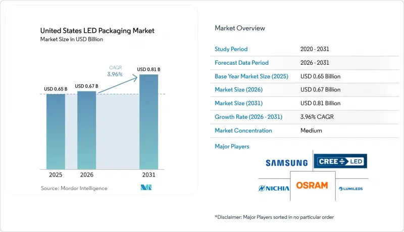
據 Mordor Intelligence 稱,2025 年美國LED構裝市值為 6.5 億美元,預計到 2031 年將達到 8.1 億美元,而 2026 年為 6.7 億美元,2026 年至 2031 年預測期內的複合年成長率為 3.96%。
本報告按封裝類型(SMD、COB、CSP、覆晶、DIP 等)、功率等級(低功率、中功率等)、發光類型(可見光LED構裝等)、材料化學性質(基板、封裝等)和應用領域(通用照明、汽車照明、顯示器和背光等)進行細分。市場預測以美元計價。
美國LED構裝市場趨勢與洞察
微型LED背光燈的應用正在迅速增加。
三星和LG發表了RGB mini-LED電視,其調光區域超過1000個,LED數量是傳統側入式LED電視的三倍。由於LED間距的縮小,需要採用小於1平方毫米的晶片級封裝,以及每小時產能超過10萬片的自動化貼片設備,並採用增強型散熱通孔,以確保結溫低於85 度C,從而保證產品在整個生命週期內的色彩穩定性。供應鏈的學習曲線使得mini-LED電視的平均價格在過去一年中下降了近30%,使其從高階市場轉向中階市場。對於LED構裝製造商而言,這種架構提高了單面板的效益,因為它以獨立的紅色、綠色、藍色三色晶片取代了白光LED和量子點薄膜。加州和德克薩斯州的消費性電子組裝廠對這種技術的需求最高,因為這些地區較短的設計週期更有利於能夠快速交付的國內供應商。這種轉變也推動了對低翹曲金屬芯基板的投資,以散發高像素密度陣列中熱點的熱量。
加強美國對固體照明(SSL)的能源效率標準。
2024年4月,美國能源局最終確定了相關法規,要求通用照明燈具的最低光通量效率在2028年7月前達到約120 lm/W。這將有效地淘汰大多數非LED技術。因此, LED構裝製造商必須提高磷光體的轉換效率,並採用低熱阻覆晶設計,以在不發生色偏的情況下維持高驅動電流。整合式燈具現在還需要滿足0.7或更高的功率因數標準,這意味著封裝的散熱設計和電子驅動器的性能密切相關。對於高顯色性(CRI)和可調色溫產品,最佳化方面的權衡變得更加嚴格,促使企業開發出細分的產品線,區分專注於符合法規要求的型號和人性化照明產品。從長遠來看,這些法規將有助於維持穩定的替換需求基礎,並保護LED構裝市場免受新建專案支出週期性波動的影響。
先進的包裝生產線需要大量的初始資本投入。
用於覆晶鍵合、晶片級封裝 (CSP)組裝和自動光學檢測 (AOI) 的設備部署,每個生產基地需要投資 3,000 萬至 8,000 萬美元。設備前置作業時間通常超過 12 個月,只有少數幾家全球供應商能夠提供共晶晶片貼裝爐、晶圓級磷光體塗覆設備和小於 0.2 毫米的拾取系統。儘管「CHIPS for America」計畫已撥款 14 億美元用於先進封裝的試點生產線,但預計高利潤的微電子領域將比 LED 產品更早啟動初始量產。因此,許多區域性封裝公司將關鍵工序外包給東亞的分包商,承擔了物流成本和關稅波動的風險。對於那些希望瞄準汽車和園藝等高可靠性細分市場的美國小規模參與企業,獲得價格合理的資金仍然是最大的障礙。
細分市場分析
晶片級封裝正以4.44%的複合年成長率快速擴張,成為成長最快的封裝類型,這主要得益於電視製造商和汽車OEM廠商對亞毫米級封裝尺寸的需求,以減少光損耗並簡化組裝。同時,表面黏著型元件(SMD)封裝憑藉其廣泛的可用性和成熟的貼片基礎設施,預計到2025年仍將佔據LED構裝市場41.38%的最大佔有率。
隨著小間距Mini-LED背光和像素化頭燈的普及,人們對覆晶結構的興趣日益濃厚。這種結構無需頂部電極,可將結到外殼的熱阻降低高達40%。同時,在需要連續高光通量和均勻色彩輸出的商用下照燈和花園照明燈具中,板載晶片(COB)模組仍然發揮著重要作用。雙列直插式封裝和通孔封裝仍在維修標牌市場中使用,但隨著自動化表面黏著技術製程的普及,它們的市場佔有率正在萎縮。在LED構裝市場,整合矩陣元件和玻璃基板封裝(將驅動IC、散熱器和光學元件共同封裝,用於高度整合的顯示器)的出現,標誌著半導體製造和印刷基板製造的融合趨勢。
到2025年,中功率元件將占美國LED構裝市場價值的36.83%。這是因為中功率元件能夠以較低的成本滿足常見的A類燈具和照明燈具的要求,但日益嚴格的光通量效率法規正促使高亮度封裝產品走向整合。因此,預計高功率模組(1-3瓦)將以4.21%的複合年成長率成長,超過整體LED構裝市場的成長速度,這主要得益於需要持續光通量的應用,例如路燈維修、園藝照明燈具和汽車自我調整光束燈。
功率超過3W的高功率燈具,其表面熱通量密度接近85W/cm²,因此採用氮化鋁陶瓷、均熱板散熱器和主動冷卻策略至關重要。同時,由於最低流明基準值的不斷提高,低功率產品在通用燈具市場的重要性正在下降。隨著驅動電流的增加,研發投入正轉向高可靠性的銀燒結晶片黏接技術和高導熱性的磷光體-矽複合材料,以確保即使在汽車和園藝應用中,結溫在工作循環期間超過100 度C時,燈具仍能保持性能。
其他好處:
- Excel格式的市場預測(ME)表
- 3個月的分析師支持
目錄
第1章:引言
- 研究假設、市場定義
- 調查範圍
第2章:調查方法
第3章執行摘要
第4章 市場狀況
- 市場概覽
- 產業價值鏈分析
- 技術分析
- 監理情勢
- 宏觀經濟因素對市場的影響
- 市場促進因素
- Mini-LED背光燈的應用正在快速成長。
- 加強美國固體照明能源效率標準
- 汽車LED在ADAS感測器中的快速應用
- 受控環境農業中園藝照明的擴展
- 政府採取措施促進半導體封裝產業回歸日本
- 矽光電整合封裝技術的突破性進展
- 市場限制因素
- 先進包裝生產線的初始資本投資成本較高
- 與覆晶製程相關的智慧財產權訴訟風險
- 磷光體稀土元素鏈的不穩定性
- 高功率水準下的溫度控管挑戰
- 波特五力分析
第5章 市場規模與成長預測
- 按包裝類型
- 表面黏著型元件(SMD)
- 板載晶片(COB)
- 晶片級封裝(CSP)
- 覆晶LED構裝
- 雙列直插封裝(DIP/通孔)
- 其他 - IMD、GOB、Mini-LED 顯示封裝
- 按電力等級
- 低功率(小於0.5瓦)
- 中功率(0.5–1 瓦)
- 高功率(1-3瓦)
- 高功率(超過 3 瓦)
- 按發光類型
- 可見光LED構裝
- 紅外線(IR) LED構裝
- 紫外線 (UV) LED構裝
- 材料化學
- 基材
- 封裝
- 黏接/晶片貼裝
- 磷光體/塗層
- 透過使用
- 一般照明
- 汽車照明
- 顯示器和背光
- 家用電子產品
- 工業和專業應用
第6章 競爭情勢
- 市場集中度分析
- 策略趨勢
- 市佔率分析
- 公司簡介
- Wolfspeed Inc.
- Lumileds Holding BV
- Nichia Corporation
- Osram Opto Semiconductors GmbH
- Samsung Electronics Co., Ltd.(Samsung LED)
- Seoul Semiconductor Co., Ltd.
- LG Innotek Co., Ltd.
- Everlight Electronics Co., Ltd.
- Bridgelux Inc.
- Cree LED, an SGH Company
- Lite-On Technology Corporation
- Stanley Electric Co., Ltd.
- Citizen Electronics Co., Ltd.
- Epistar Corporation
- Lextar Electronics Corporation
- Dominant Opto Technologies Sdn. Bhd.
- Advanced Optoelectronic Technology Inc.
- Unity Opto Technology Co., Ltd.
- Huga Optotech Inc.
- Acuity Brands Lighting Inc.
第7章 市場機會與未來展望
According to Mordor Intelligence, the united states lED packaging market size was valued at USD 0.65 billion in 2025 and estimated to grow from USD 0.67 billion in 2026 to reach USD 0.81 billion by 2031, at a CAGR of 3.96% during the forecast period 2026-2031.
This report is Segmented by Packaging Architecture (SMD, COB, CSP, Flip-Chip, DIP, and More), Power Class (Low Power, Mid Power, and More), Emission Type (Visible LED Packages, and More), Material Chemistry (Substrates, Encapsulation, and More), and Application (General Lighting, Automotive Lighting, Display and Backlighting, and More). The Market Forecasts are Provided in Terms of Value (USD).
United States LED Packaging Market Trends and Insights
Surge In Mini-LED Backlight Adoption
Samsung and LG introduced RGB Mini-LED televisions featuring more than 1,000 dimming zones, tripling the LED count versus legacy edge-lit designs. The finer pitch demands chip scale packages under 1 mm2, automated pick-and-place tools exceeding 100,000 units per hour, and enhanced thermal vias to keep junction temperatures below 85 °C, preserving color stability over product lifetimes. Supply-chain learning curves have lowered average Mini-LED TV prices by nearly 30% over the past year, moving the technology from premium to mid-tier segments. For LED packagers, the architecture lifts revenue per panel because discrete red, green, and blue dies replace white LEDs plus quantum-dot films. Demand is strongest in consumer electronics assembly hubs in California and Texas, where rapid design cycles favor domestic suppliers capable of short lead times. The shift also stimulates investment in low-warpage metal-core printed circuit boards that dissipate hotspot heat in high-pixel-density arrays.
Tightening U.S. Energy-Efficiency Norms For Solid-State Lighting
The U.S. Department of Energy finalized a rule in April 2024 that raises general service lamp efficacy to roughly 120 lm W-1 by July 2028, effectively eliminating most non-LED technologies. LED packagers must therefore improve phosphor conversion efficiency and adopt low-thermal-resistance flip-chip designs that sustain high drive currents without color shift. Integrated lamps must now meet power-factor thresholds of 0.7 or higher, linking package thermal design with electronic driver performance. High-CRI and color-tunable products face steeper optimization trade-offs, prompting segmented product lines that separate compliance-focused models from premium human-centric lighting offerings. Over the long term, the rule supports a steady baseline of replacement demand, cushioning the LED packaging market against cyclical swings in new-construction spending.
High Initial Capex For Advanced Packaging Lines
Setting up flip-chip bonding, chip scale package assembly, and automated optical inspection requires investments of USD 30 million to USD 80 million per site. Tool lead times often exceed 12 months, and only a handful of global vendors supply eutectic die-attach ovens, wafer-level phosphor coaters, and sub-0.2 mm pick-and-place systems. Although the CHIPS for America program awarded USD 1.4 billion for advanced-packaging pilot lines, first commercial volumes will serve high-margin microelectronics long before LED products. Many regional packagers therefore outsource critical steps to subcontractors in East Asia, incurring logistics costs and exposure to tariff swings. Access to affordable capital remains the primary barrier for smaller U.S. entrants wishing to target high-reliability automotive or horticulture niches.
Other drivers and restraints analyzed in the detailed report include:
- Rapid Automotive LED Penetration In ADAS Sensors
- Expansion Of Horticulture Lighting In Controlled-Environment Farming
- IP Litigation Risks Around Flip-Chip Processes
For complete list of drivers and restraints, kindly check the Table Of Contents.
Segment Analysis
Chip scale packages account for the fastest growth trajectory, expanding at a 4.44% CAGR, as television makers and automotive OEMs demand sub-millimeter footprints that reduce optical losses and simplify assembly. Surface mount device formats still delivered the largest 41.38% LED packaging market share in 2025, supported by broad availability and well-established pick-and-place infrastructure.
The migration toward fine-pitch Mini-LED backlights and pixelated headlights is elevating interest in flip-chip architectures that eliminate top-side electrodes, trimming junction-to-case thermal resistance by up to 40%. Meanwhile, chip-on-board modules retain relevance in commercial downlights and horticulture fixtures where continuous high flux and uniform color output matter. Dual in-line and through-hole packages persist in retrofit signage but face erosion as automated surface-mount processes dominate. Integrated matrix device and glass-on-board concepts within the LED packaging market are emerging to co-package driver ICs, thermal spreaders, and optics for highly integrated displays, signaling a convergence of semiconductor and printed-circuit manufacturing disciplines.
Mid-power devices held 36.83% of the United States LED packaging market in 2025 value because they satisfy typical A-lamp and troffer requirements at modest cost, yet tightening efficacy rules favor consolidation into fewer, brighter packages. High-power modules (1-3 W) are therefore projected to outpace the overall LED packaging market size with a 4.21% CAGR, fueled by street-lighting retrofits, horticulture luminaires, and adaptive automotive beams that require sustained luminous flux.
Ultra-high-power units above 3 W confront thermal flux densities near 85 W cm-2, compelling adoption of aluminum-nitride ceramics, vapor-chamber heat spreaders, and active cooling strategies. At the opposite end, low-power indicators lose relevance in general service lamps as minimum lumen thresholds rise. Rising drive currents are also directing R&D dollars toward high-reliability silver-sintered die attach and high-thermal-conductivity phosphor-silicone composites, maintaining performance even when junctions surpass 100 °C during automotive or horticultural duty cycles.
List of Companies Covered in this Report:
- Wolfspeed Inc.
- Lumileds Holding B.V.
- Nichia Corporation
- Osram Opto Semiconductors GmbH
- Samsung Electronics Co., Ltd. (Samsung LED)
- Seoul Semiconductor Co., Ltd.
- LG Innotek Co., Ltd.
- Everlight Electronics Co., Ltd.
- Bridgelux Inc.
- Cree LED, an SGH Company
- Lite-On Technology Corporation
- Stanley Electric Co., Ltd.
- Citizen Electronics Co., Ltd.
- Epistar Corporation
- Lextar Electronics Corporation
- Dominant Opto Technologies Sdn. Bhd.
- Advanced Optoelectronic Technology Inc.
- Unity Opto Technology Co., Ltd.
- Huga Optotech Inc.
- Acuity Brands Lighting Inc.
Additional Benefits:
- The market estimate (ME) sheet in Excel format
- 3 months of analyst support
TABLE OF CONTENTS
1 INTRODUCTION
- 1.1 Study Assumptions, Market Definition
- 1.2 Scope of the Study
2 RESEARCH METHODOLOGY
3 EXECUTIVE SUMMARY
4 MARKET LANDSCAPE
- 4.1 Market Overview
- 4.2 Industry Value-Chain Analysis
- 4.3 Technology Analysis
- 4.4 Regulatory Landscape
- 4.5 Impact of Macroeconomic Factors on the Market
- 4.6 Market Drivers
- 4.6.1 Surge in Mini-LED Backlight Adoption
- 4.6.2 Tightening U.S. Energy-Efficiency Norms for Solid-State Lighting
- 4.6.3 Rapid Automotive LED Penetration in ADAS Sensors
- 4.6.4 Expansion of Horticulture Lighting in Controlled-Environment Farming
- 4.6.5 Government On-shoring Incentives for Semiconductor Packaging
- 4.6.6 Breakthroughs in Silicon Photonics Integrated Packaging
- 4.7 Market Restraints
- 4.7.1 High Initial Capex for Advanced Packaging Lines
- 4.7.2 IP Litigation Risks Around Flip-Chip Processes
- 4.7.3 Volatility in Phosphor Rare-Earth Supply Chain
- 4.7.4 Thermal-Management Challenges at Ultra-High Power Levels
- 4.8 Porter's Five Forces Analysis
- 4.8.1 Bargaining Power of Suppliers
- 4.8.2 Bargaining Power of Buyers
- 4.8.3 Threat of New Entrants
- 4.8.4 Threat of Substitutes
- 4.8.5 Intensity of Competitive Rivalry
5 MARKET SIZE AND GROWTH FORECASTS (VALUE)
- 5.1 By Packaging Architecture
- 5.1.1 Surface Mount Device (SMD)
- 5.1.2 Chip-on-Board (COB)
- 5.1.3 Chip Scale Package (CSP)
- 5.1.4 Flip-Chip LED Packages
- 5.1.5 Dual In-line Package (DIP / Through-hole)
- 5.1.6 Others - IMD, GOB, Mini-LED Display Packaging
- 5.2 By Power Class
- 5.2.1 Low Power (Less Than 0.5 W)
- 5.2.2 Mid Power (0.5 to 1 W)
- 5.2.3 High Power (1 to 3 W)
- 5.2.4 Ultra-High Power (More Than 3 W)
- 5.3 By Emission Type
- 5.3.1 Visible LED Packages
- 5.3.2 Infrared (IR) LED Packages
- 5.3.3 Ultraviolet (UV) LED Packages
- 5.4 By Material Chemistry
- 5.4.1 Substrates
- 5.4.2 Encapsulation
- 5.4.3 Bonding / Die-Attach
- 5.4.4 Phosphors / Coatings
- 5.5 By Application
- 5.5.1 General Lighting
- 5.5.2 Automotive Lighting
- 5.5.3 Display and Backlighting
- 5.5.4 Consumer Electronics
- 5.5.5 Industrial and Specialty
6 COMPETITIVE LANDSCAPE
- 6.1 Market Concentration Analysis
- 6.2 Strategic Moves
- 6.3 Market Share Analysis
- 6.4 Company Profiles (includes Global Level Overview, Market Level Overview, Core Segments, Financials as available, Strategic Information, Market Rank/Share, Products and Services, Recent Developments)
- 6.4.1 Wolfspeed Inc.
- 6.4.2 Lumileds Holding B.V.
- 6.4.3 Nichia Corporation
- 6.4.4 Osram Opto Semiconductors GmbH
- 6.4.5 Samsung Electronics Co., Ltd. (Samsung LED)
- 6.4.6 Seoul Semiconductor Co., Ltd.
- 6.4.7 LG Innotek Co., Ltd.
- 6.4.8 Everlight Electronics Co., Ltd.
- 6.4.9 Bridgelux Inc.
- 6.4.10 Cree LED, an SGH Company
- 6.4.11 Lite-On Technology Corporation
- 6.4.12 Stanley Electric Co., Ltd.
- 6.4.13 Citizen Electronics Co., Ltd.
- 6.4.14 Epistar Corporation
- 6.4.15 Lextar Electronics Corporation
- 6.4.16 Dominant Opto Technologies Sdn. Bhd.
- 6.4.17 Advanced Optoelectronic Technology Inc.
- 6.4.18 Unity Opto Technology Co., Ltd.
- 6.4.19 Huga Optotech Inc.
- 6.4.20 Acuity Brands Lighting Inc.
7 MARKET OPPORTUNITIES AND FUTURE OUTLOOK
- 7.1 White-Space and Unmet-Need Assessment

 LED構裝測試設備市場:全球市場預測,2026-2032年晶片級封裝 (CSP) LED 市場:2026-2032 年全球市場預測(按產品類型、顏色類型、功率等級、應用、終端用戶產業和分銷管道分類)
 歐洲LED構裝:市場佔有率分析、產業趨勢與統計及成長預測(2026-2031年)
 全球LED構裝市場規模、佔有率、趨勢及成長分析報告(2026-2034年)
 LED構裝市場規模、佔有率和趨勢分析報告:按材料、封裝類型、應用、地區和細分市場分類(2026-2033年)LED構裝設備:市場佔有率分析、產業趨勢與統計、成長預測(2026-2031年)LED構裝:市場佔有率分析、產業趨勢與統計、成長預測(2026-2031年)中國LED構裝:市佔率分析、產業趨勢與統計及成長預測(2026-2031年)北美LED構裝:市佔率分析、產業趨勢與統計及成長預測(2026-2031年)亞太地區LED構裝:市佔率分析、產業趨勢與統計及成長預測(2026-2031年)