


 |
市場調查報告書
商品編碼
2122645
半導體化學氣相沉積設備:市場佔有率分析、產業趨勢與統計、成長預測(2026-2031)Semiconductor CVD Equipment - Market Share Analysis, Industry Trends & Statistics, Growth Forecasts (2026 - 2031) |
||||||

※ 本網頁內容可能與最新版本有所差異。詳細情況請與我們聯繫。
據 Mordor Intelligence 稱,半導體 CVD 設備市場預計在 2026 年達到 167.1 億美元,預計到 2031 年將達到 219.6 億美元,在預測期(2026-2031 年)內以 5.62% 的複合年成長率成長。
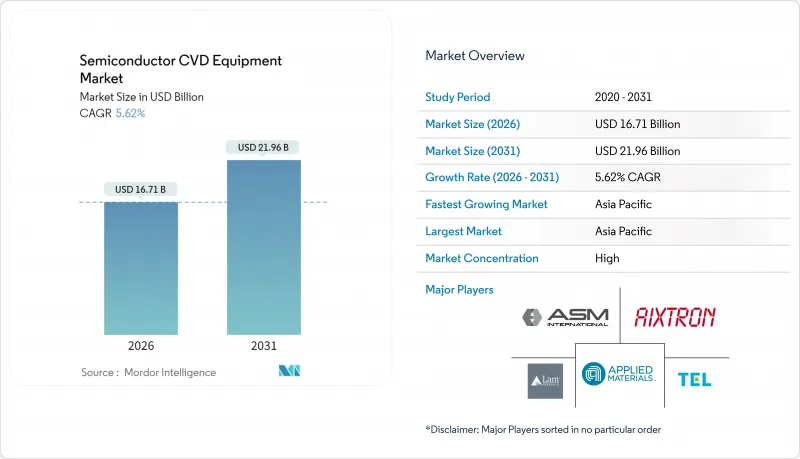
本報告按應用領域(代工廠、整合裝置製造商、功率元件和模擬器零件工廠等)、CVD技術類型(等離子增強CVD、低壓CVD等)、設備配置(單晶圓叢集等)、晶圓尺寸(150mm以下等)、最終用戶類型(純代工廠等)和地區進行細分。市場預測以美元計價。
全球半導體CVD設備市場趨勢及洞察
2nm 以下邏輯節點的競爭日益激烈,推動了 ALD 和 CVD 設備數量的成長。
在2奈米或更小的環柵(GaA)架構中,沉積製程比傳統FinFET複雜40-50%,每片晶圓的設備使用頻率也高出約1.8倍。台積電的N2製程於2025年下半年開始量產,採用循環等離子體增強原子層沉積(ALD)技術製備高介電常數材料,並採用選擇性鎢化學氣相沉積(CVD)技術製備電極;三星則整合了背面供電功能,形成了一種可重複進行平坦化和再沉積循環的機制。英特爾的18A節點計劃於2026年下半年部署,它結合了RibbonFET和PowerVia功能,需要一個能夠在單一真空環境下切換熱模式和等離子體模式的混合ALD-CVD腔室。因此,每個最先進的晶圓廠都需要購買80-100個製程腔室,這將導致每個廠址額外增加20-30億美元的沉積成本。
用於電動車和可再生能源的SiC/GaN功率元件的資本投資正在激增。
Wolfspeed、英飛凌和安森美半導體都已開始興建200毫米碳化矽(SiC)晶圓廠,這三家公司2025年的資本支出計畫合計超過100億美元。由於SiC漂移層的成長速度仍受到產能的限制,因此金屬有機化學氣相沉積(MOCVD)反應器約佔這些預算的四分之一。氮化鎵(GaN)在資料中心電源的應用日益廣泛,使得化合物半導體代工廠的產運轉率達到85%,從而引發了對AIXTRON行星式反應器的長期設備訂單。預計到2030年,寬能隙晶圓的開工量將以每年18%的速度成長,半導體CVD設備市場的需求預計將轉向專用MOCVD平台。
超過 5000 萬歐元的設備價格和較長的投資回報率回收期阻礙了中小鑄造廠的參與。
用於環柵(GAA)邏輯的原子層沉積(ALD)叢整合本超過5000萬歐元(5650萬美元),並且需要額外簽訂年度服務契約,費用相當於初始投資的8%至12%。因此,專注於成熟製程節點的公司正在將翻新的PECVD腔室的有效使用壽命延長至12年,減緩了設備的更換速度。由於資本密集度的差異,全球78%的薄膜沉積設備採購集中在前十大製造商手中,造成了客戶格局的兩極化,並限制了二線晶圓廠的擴張。
細分市場分析
隨著台積電和三星逐步實現3奈米和2奈米製程的量產,預計到2025年,晶圓代工業務將佔總收入的41.64%,成為半導體CVD設備市場的基礎。在所有應用領域中,功率元件和模擬器元件預計將以6.04%的複合年成長率(CAGR)實現最高成長,因為電動車和可再生能源轉換器需要採用低壓CVD技術製備的厚外延層。記憶體佔19%,但隨著3D-NAND快閃記憶體的微型化,其裝置集中度成長最為迅速。整合設備製造商佔23%,他們既使用單晶圓叢集進行邏輯電路生產,也使用批量爐進行成本控制的類比電路生產。 LED和光電子裝置目前仍處於小眾領域,佔6%,但隨著微型LED和雷射雷達(LiDAR)的普及,其成長勢頭強勁。
預計到2031年,晶圓代工廠將維持約40%的市場佔有率,但隨著成熟製程節點更多地轉向現有設備的維修而非新平台的購置,成長速度預計將會放緩。相較之下,德國、美國和馬來西亞的功率元件產能正在快速擴張,推動了對用於特殊應用的MOCVD技術的需求。記憶體領域的投資仍呈現週期性波動,因為它受到HBM和NAND價格走勢的影響。與LED生產相關的半導體化學氣相沉積設備的市場規模預計將根據擴增實境(AR)顯示器的發展藍圖波動。
到2025年,單晶圓叢集將佔部署總量的45.09%,為所有尖端邏輯和記憶體藍圖提供支援。同時,批量立式爐預計將在28奈米和40奈米模擬晶圓廠中以6.18%的複合年成長率成長,因為它們能以犧牲製程精度為代價,將每片晶圓的成本降低40-50%。雙腔叢集透過平衡產能和柔軟性,將佔18%的佔有率,而行星式反應器將佔12%,主要用於化合物半導體的MOCVD領域。其餘部分則由傳統的單腔和中試系統組成。
環柵(GaA)元件的晶圓均勻性已達到1%以下,鞏固了單片晶圓在尖端領域的重要性。然而,成熟節點仍佔據全球晶圓供應量的72%,而垂直反應器在±5%公差即可滿足要求的領域正在重新奪回市場構成比。雙腔體設計在混合原子層沉積-化學氣相沉積(ALD-CVD)堆疊結構中日益普及,可將週期時間縮短30%。行星式反應器在LED外延領域仍具有競爭力,但在GaN功率元件領域正面臨單晶片晶圓技術的挑戰。
區域分析
預計到2025年,亞太地區將佔全球銷售額的47.57%,並在2031年之前維持7.83%的複合年成長率。這主要得益於台積電、三星和SK海力士每月增加100萬片晶圓的先進元件和功率元件產能。儘管有出口限制,但中國市場對成熟製程節點的需求依然強勁,NAURA Technology和AMEC的市佔率已增至22%。日本提供的2兆日圓補貼確保了台積電熊本工廠和美光廣島工廠的擴建。在東南亞,後端和功率元件領域的投資持續湧入,其中包括英飛凌在馬來西亞建設的200毫米碳化矽生產線。
預計到2025年,北美將佔全球銷售額的28%,這主要得益於一項價值527億美元的CHIPS撥款,該撥款支持英特爾、德克薩斯德州儀器等公司的擴張。然而,由於許可核准延遲,一些美國晶圓廠的竣工日期被推遲到2027-2028年,而且許多項目都瞄準了成熟節點、設備密集度較低的模擬晶片生產,導致其預計複合年成長率僅為5.2%,低於亞太地區。加拿大的矽光電系統和墨西哥新興的晶圓級封裝(WLP)生產線正在催生小眾但快速成長的需求。
預計到2025年,歐洲將佔全球銷售額的18%,並將以每年4.8%的速度持續成長至2031年。英特爾位於馬德堡的價值300億歐元(350.7億美元)的工廠、台積電位於德累斯頓的價值100億歐元(116.9億美元)的合資企業以及英飛凌價值50億歐元(58.4億美元)的PowerFab工廠是推動短期訂單成長的主要動力。更嚴格的環保法規將強制要求對排放氣體進行原位處理,這將使PECVD系統的成本增加15%至20%。中東、非洲和南美洲的市佔率總合不足7%,但如果阿布達比晶圓廠的建設計畫和巴西政府資助的生產線得以實現,則有望創造額外的需求。
其他好處:
- Excel格式的市場預測(ME)表
- 3個月的分析師支持
目錄
第1章:引言
- 研究假設和市場定義
- 調查範圍
第2章:調查方法
第3章執行摘要
第4章 市場狀況
- 市場概覽
- 市場促進因素
- 2nm 和 2nm 以下邏輯節點市場的競爭日益激烈,推動了 ALD 和 CVD 設備安裝數量的增加。
- 用於電動車和可再生能源的SiC/GaN功率元件的資本投資正在激增。
- 層數少於 400 層的 3D-NAND 的發展藍圖需要超高 AR 間隙填充系統。
- 由於 CHIPS獎勵,全球新建的待開發區製造項目不到 30 個。
- 人工智慧驅動的製程控制正在降低成本,從而導致維修的需求增加。
- 強制在晶圓廠外能源回收將使低排放量的PECVD生產線獲得優勢。
- 市場限制因素
- 5,000 萬歐元的設備成本和較長的投資報酬率回收期阻礙了中小鑄造廠的參與。
- 中美之間的出口限制導致超過 15% 的市佔率受到限制。
- 用於 III-V 族外延的高純度金屬有機前驅體供不應求
- 逐步淘汰氟化氣體引發了代價高昂的工藝改造。 *
- 產業價值鏈分析
- 監理情勢
- 技術展望
- 波特五力分析
- 投資分析
第5章 市場規模與成長預測
- 透過使用
- 鑄造廠
- IDM
- 記憶體製造商
- 電源和模擬裝置製造廠
- LED和光電子學
- 透過設備配置
- 單晶圓叢集
- 批次立爐
- 雙腔叢集
- 行星式多晶片反應器
- 按晶圓尺寸
- 150毫米或更小
- 200 mm
- 300 mm
- 450 mm
- 按最終用戶類型分類
- 專業鑄造廠
- 垂直整合的設備製造商
- 記憶體製造商
- 無廠半導體公司及研發機構
- 按地區
- 北美洲
- 美國
- 加拿大
- 墨西哥
- 南美洲
- 巴西
- 阿根廷
- 其他南美國家
- 歐洲
- 德國
- 英國
- 法國
- 義大利
- 西班牙
- 其他歐洲國家
- 亞太地區
- 中國
- 日本
- 印度
- 韓國
- ASEAN
- 其他亞太國家
- 中東
- 沙烏地阿拉伯
- 阿拉伯聯合大公國
- 其他中東國家
- 非洲
- 南非
- 奈及利亞
- 其他非洲國家
- 北美洲
第6章 競爭情勢
- 市場集中度
- 策略趨勢
- 市佔率分析
- 公司簡介
- Applied Materials, Inc.
- Lam Research Corporation
- Tokyo Electron Limited
- ASM International NV
- AIXTRON SE
- Veeco Instruments Inc.
- ULVAC, Inc.
- Kokusai Electric Corporation
- Advanced Micro-Fabrication Equipment Inc. China
- NAURA Technology Group Co., Ltd.
- Wonik IPS Co., Ltd.
- Eugene Technology Co., Ltd.
- Jusung Engineering Co., Ltd.
- TES Co., Ltd.
- SPTS Technologies Ltd.
- CVD Equipment Corporation
- Piotech Co., Ltd.
- Plasma-Therm LLC
- Oxford Instruments plc
- Taiyo Nippon Sanso Corporation
- Topecsh Co., Ltd.
- TDK Corporation
- Lumichem Korea Co., Ltd.
第7章 市場機會與未來展望
According to Mordor Intelligence, the semiconductor CVD equipment market size is estimated at USD 16.71 billion in 2026, and is expected to reach USD 21.96 billion by 2031, at a CAGR of 5.62% during the forecast period (2026-2031).
This report is Segmented by Application (Foundry, IDM, Power and Analog Device Fabs, and More), CVD Technology Type (Plasma-Enhanced CVD, Low-Pressure CVD, and More), Equipment Configuration (Single-Wafer Cluster, and More), Wafer Size (Less Than or Equal To 150 Mm, and More), End-User Type (Pure-Play Foundries, and More), and Geography. The Market Forecasts are Provided in Terms of Value (USD).
Global Semiconductor CVD Equipment Market Trends and Insights
Intensifying 2 nm And Below Logic-Node Race Drives Higher ALD And CVD Tool Counts
Gate-all-around architectures below the 2-nanometer threshold add 40-50% more deposition steps than FinFET predecessors, lifting tool intensity per wafer starts by roughly 1.8x. TSMC's N2 process, in high-volume manufacturing since late 2025, relies on cyclic plasma-enhanced ALD for high-k dielectrics and selective tungsten CVD for contacts, whereas Samsung integrates backside power delivery that inserts repeat planarization-and-re-deposit loops. Intel's 18A node, slated for the second half of 2026, combines RibbonFET and PowerVia features that demand hybrid ALD-CVD chambers able to toggle thermal and plasma modes under a single vacuum. A single leading-edge fab therefore purchases 80-100 process chambers, resulting in USD 2-3 billion in incremental deposition spend per site.
Explosive SiC/GaN Power-Device Capex For EV And Renewables
Wolfspeed, Infineon, and onsemi each broke ground on 200-millimeter silicon carbide fabs that, together, exceeded USD 10 billion in 2025 capital plans. Metal-organic CVD reactors constitute roughly one-quarter of those budgets because SiC drift-layer growth rates remain throughput-limited. Gallium-nitride adoption in data-center power supplies has pushed compound-semiconductor foundries to 85% utilization, triggering long-term equipment orders for AIXTRON planetary reactors. With wide-bandgap wafer starts set to rise 18% annually through 2030, the semiconductor CVD equipment market will see demand tilt toward specialized metal-organic platforms.
EUR 50 Million-Plus Tool Price And Long ROIC Deter Smaller Foundries
Atomic-layer-deposition clusters configured for gate-all-around logic list above EUR 50 million (USD 56.5 million) and carry annual service contracts worth an additional 8-12% of the initial spend. Mature-node specialists, therefore, extend the effective life of refurbished PECVD chambers to 12 years, slowing replacement velocity. Capital-intensity disparity concentrates 78% of global deposition purchases among the top-10 manufacturers, creating a two-tier customer landscape that tempers expansion at second-tier fabs.
Other drivers and restraints analyzed in the detailed report include:
- 3D-NAND Less than 400-Layer Roadmaps Need Ultra-High-AR Gap-Fill Systems
- CHIPS-Style Incentives Spawning Less than 30 New Green-Field Fabs Worldwide
- U.S.-China Export Controls Limit Addressable Sales In Greater than or Equal to 15% Of Market
For complete list of drivers and restraints, kindly check the Table Of Contents.
Segment Analysis
Foundry operations generated 41.64% of 2025 revenue as TSMC and Samsung ramped 3 nanometer and 2 nanometer nodes, anchoring the semiconductor CVD equipment market. Power and analog fabs are projected to advance at a 6.04% CAGR, the highest among applications, as electric vehicles and renewable-energy converters require thick epitaxial layers formed by low-pressure CVD. Memory accounted for 19% but sees the steepest tool-intensity gains from 3D-NAND scaling. Integrated device manufacturers contributed 23%, balancing single-wafer clusters for logic with batch furnaces for cost-sensitive analog lines. LED and optoelectronics remain niche at 6% yet gain momentum from micro-LED and LiDAR adoption.
Foundries are expected to maintain roughly 40% share through 2031, but growth moderates because mature-node lines increasingly retrofit existing chambers rather than purchase new platforms. In contrast, power-device capacity is expanding aggressively in Germany, the United States, and Malaysia, lifting specialty MOCVD demand. Memory spending remains cyclical, hinging on HBM and NAND pricing. The semiconductor chemical vapor deposition equipment market size tied to LED production will fluctuate with augmented-reality display roadmaps.
Single-wafer clusters accounted for 45.09% of 2025 installations, underpinning every leading-edge logic and memory roadmap. Batch vertical furnaces, however, are expected to grow at a 6.18% CAGR as 28-nanometer and 40-nanometer analog fabs trade process precision for 40-50% lower cost per wafer. Dual-chamber clusters accounted for 18% by blending throughput with flexibility, while planetary reactors accounted for 12%, largely in compound-semiconductor MOCVD. Legacy single-chamber and pilot tools filled the remainder.
Gate-all-around devices achieve within-wafer uniformity of less than or equal to 1%, cementing single-wafer relevance at the frontier. Still, the global wafer-start mix remains 72% mature nodes, allowing vertical furnaces to reclaim share where +-5% tolerance suffices. Dual-chamber designs are gaining popularity for hybrid ALD-CVD stacks, shaving 30% off cycle time. Planetary reactors stay competitive in LED epitaxy but face single-wafer encroachment for GaN power devices.
Complete Report Scope:
- By Application
- Foundry
- IDM
- Memory Manufacturers
- Power and Analog Device Fabs
- LEDs and Optoelectronics
- By Equipment Configuration
- Single-Wafer Cluster
- Batch Vertical Furnace
- Dual-Chamber Cluster
- Planetary Multi-Wafer Reactor
- By Wafer Size
- Less Than or Equal to 150 mm
- 200 mm
- 300 mm
- 450 mm
- By End-User Type
- Pure-Play Foundries
- Integrated Device Manufacturers
- Memory Companies
- Fabless and R&D Institutes
- By Geography
- North America
- United States
- Canada
- Mexico
- South America
- Brazil
- Argentina
- Rest of South America
- Europe
- Germany
- United Kingdom
- France
- Italy
- Spain
- Rest of Europe
- Asia-Pacific
- China
- Japan
- India
- South Korea
- ASEAN
- Rest of Asia-Pacific
- Middle East
- Saudi Arabia
- United Arab Emirates
- Rest of Middle East
- Africa
- South Africa
- Nigeria
- Rest of Africa
- North America
Geography Analysis
Asia-Pacific retained 47.57% of 2025 revenue and is projected to deliver a 7.83% CAGR through 2031 as TSMC, Samsung, and SK Hynix add 1 million wafer starts per month of leading-edge and power capacity. Chinese mature-node demand persists despite export controls, with NAURA Technology and AMEC lifting their local share to 22%. Japan's JPY 2 trillion subsidy pool secures both TSMC's Kumamoto and Micron's Hiroshima expansions. Southeast Asia continues to absorb back-end and power-device investments, including Infineon's 200 millimeter SiC line in Malaysia.
North America generated 28% of 2025 revenue, buoyed by USD 52.7 billion in CHIPS subsidies that anchor Intel, Micron, and Texas Instruments expansions. However, a 5.2% forecast CAGR trails Asia-Pacific because permitting delays push several U.S. fabs into 2027-2028 completion windows and because many projects target mature-node analog production with lower tool intensity. Canada's silicon-photonics ecosystem and Mexico's emerging wafer-level packaging lines add niche but growing demand.
Europe captured 18% of 2025 revenue and will expand at 4.8% through 2031. Intel's EUR 30 billion (USD 35.07 billion) Magdeburg fab, TSMC's EUR 10 billion (USD 11.69 billion) Dresden joint venture, and Infineon's EUR 5 billion (USD 5.84 billion) PowerFab drive near-term orders. Strict environmental mandates raise PECVD system costs by 15-20% as in-situ abatement becomes compulsory. The Middle East and Africa and South America collectively hold less than 7% but may unlock incremental demand should proposed fabs in Abu Dhabi or government-funded Brazilian lines proceed.
- Applied Materials, Inc.
- Lam Research Corporation
- Tokyo Electron Limited
- ASM International N.V.
- AIXTRON SE
- Veeco Instruments Inc.
- ULVAC, Inc.
- Kokusai Electric Corporation
- Advanced Micro-Fabrication Equipment Inc. China
- NAURA Technology Group Co., Ltd.
- Wonik IPS Co., Ltd.
- Eugene Technology Co., Ltd.
- Jusung Engineering Co., Ltd.
- TES Co., Ltd.
- SPTS Technologies Ltd.
- CVD Equipment Corporation
- Piotech Co., Ltd.
- Plasma-Therm LLC
- Oxford Instruments plc
- Taiyo Nippon Sanso Corporation
- Topecsh Co., Ltd.
- TDK Corporation
- Lumichem Korea Co., Ltd.
Additional Benefits:
- The market estimate (ME) sheet in Excel format
- 3 months of analyst support
TABLE OF CONTENTS
1 INTRODUCTION
- 1.1 Study Assumptions and Market Definition
- 1.2 Scope of the Study
2 RESEARCH METHODOLOGY
3 EXECUTIVE SUMMARY
4 MARKET LANDSCAPE
- 4.1 Market Overview
- 4.2 Market Drivers
- 4.2.1 Intensifying 2 Nm-And-Below Logic Node Race Drives Higher ALD + CVD Tool Counts
- 4.2.2 Explosive SIC/GaN Power-Device Capex For EV and Renewables
- 4.2.3 3D-NAND Less Than 400-Layer Roadmaps Need Ultra-High-AR Gap-Fill Systems
- 4.2.4 CHIPS-Style Incentives Spawning Less Than 30 New Green-Field Fabs Worldwide
- 4.2.5 AI-Enabled Process-Control Lowers Coo, Boosting Retrofit Demand
- 4.2.6 Sub-Fab Energy-Recovery Mandates Favour Low-Emission PECVD Lines*
- 4.3 Market Restraints
- 4.3.1 EUR 50 Million Tool Price And Long ROIC Deter Smaller Foundries
- 4.3.2 U.S.-China Export Controls Limit Addressable Sales In Greater than 15% Of Market
- 4.3.3 Scarcity Of High-Purity Metal-Organic Precursors For III-V Epi
- 4.3.4 F-Gas Phase-Out Rules Trigger Costly Process Redesigns*
- 4.4 Industry Value Chain Analysis
- 4.5 Regulatory Landscape
- 4.6 Technological Outlook
- 4.7 Porter's Five Forces Analysis
- 4.7.1 Bargaining Power of Suppliers
- 4.7.2 Bargaining Power of Buyers
- 4.7.3 Threat of New Entrants
- 4.7.4 Threat of Substitute Products
- 4.7.5 Degree of Competition
- 4.8 Investment Analysis
5 MARKET SIZE AND GROWTH FORECASTS (VALUE)
- 5.1 By Application
- 5.1.1 Foundry
- 5.1.2 IDM
- 5.1.3 Memory Manufacturers
- 5.1.4 Power and Analog Device Fabs
- 5.1.5 LEDs and Optoelectronics
- 5.2 By Equipment Configuration
- 5.2.1 Single-Wafer Cluster
- 5.2.2 Batch Vertical Furnace
- 5.2.3 Dual-Chamber Cluster
- 5.2.4 Planetary Multi-Wafer Reactor
- 5.3 By Wafer Size
- 5.3.1 Less Than or Equal to 150 mm
- 5.3.2 200 mm
- 5.3.3 300 mm
- 5.3.4 450 mm
- 5.4 By End-User Type
- 5.4.1 Pure-Play Foundries
- 5.4.2 Integrated Device Manufacturers
- 5.4.3 Memory Companies
- 5.4.4 Fabless and R&D Institutes
- 5.5 By Geography
- 5.5.1 North America
- 5.5.1.1 United States
- 5.5.1.2 Canada
- 5.5.1.3 Mexico
- 5.5.2 South America
- 5.5.2.1 Brazil
- 5.5.2.2 Argentina
- 5.5.2.3 Rest of South America
- 5.5.3 Europe
- 5.5.3.1 Germany
- 5.5.3.2 United Kingdom
- 5.5.3.3 France
- 5.5.3.4 Italy
- 5.5.3.5 Spain
- 5.5.3.6 Rest of Europe
- 5.5.4 Asia-Pacific
- 5.5.4.1 China
- 5.5.4.2 Japan
- 5.5.4.3 India
- 5.5.4.4 South Korea
- 5.5.4.5 ASEAN
- 5.5.4.6 Rest of Asia-Pacific
- 5.5.5 Middle East
- 5.5.5.1 Saudi Arabia
- 5.5.5.2 United Arab Emirates
- 5.5.5.3 Rest of Middle East
- 5.5.6 Africa
- 5.5.6.1 South Africa
- 5.5.6.2 Nigeria
- 5.5.6.3 Rest of Africa
- 5.5.1 North America
6 COMPETITIVE LANDSCAPE
- 6.1 Market Concentration
- 6.2 Strategic Moves
- 6.3 Market Share Analysis
- 6.4 Company Profiles (includes Global-level Overview, Market-level Overview, Core Segments, Financials as available, Strategic Information, Market Rank/Share, Products and Services, Recent Developments)
- 6.4.1 Applied Materials, Inc.
- 6.4.2 Lam Research Corporation
- 6.4.3 Tokyo Electron Limited
- 6.4.4 ASM International N.V.
- 6.4.5 AIXTRON SE
- 6.4.6 Veeco Instruments Inc.
- 6.4.7 ULVAC, Inc.
- 6.4.8 Kokusai Electric Corporation
- 6.4.9 Advanced Micro-Fabrication Equipment Inc. China
- 6.4.10 NAURA Technology Group Co., Ltd.
- 6.4.11 Wonik IPS Co., Ltd.
- 6.4.12 Eugene Technology Co., Ltd.
- 6.4.13 Jusung Engineering Co., Ltd.
- 6.4.14 TES Co., Ltd.
- 6.4.15 SPTS Technologies Ltd.
- 6.4.16 CVD Equipment Corporation
- 6.4.17 Piotech Co., Ltd.
- 6.4.18 Plasma-Therm LLC
- 6.4.19 Oxford Instruments plc
- 6.4.20 Taiyo Nippon Sanso Corporation
- 6.4.21 Topecsh Co., Ltd.
- 6.4.22 TDK Corporation
- 6.4.23 Lumichem Korea Co., Ltd.
7 MARKET OPPORTUNITIES AND FUTURE OUTLOOK
- 7.1 White-space and Unmet-need Assessment

 心血管疾病(CVD)流行病學分析與預測:2026-2035年
 循環葡萄酒和飲料容器押金系統市場預測至2034年-全球分析(按容器材料、飲料類型、制度模式、相關人員參與、技術整合和區域分類)
 化學氣相沉積 (CVD) 市場規模、佔有率和趨勢分析報告:按類別、應用、地區和細分市場分類 - 預測 (2026–2033)
 化學氣相沉積設備市場報告:按技術、應用、最終用戶和地區分類(2026-2034 年)
 化學氣相沉積(CVD)市場:按技術、應用和地區分類
 LED外延MOCVD設備:市場佔有率分析、產業趨勢與統計、成長預測(2026-2031年)中國LED外延MOCVD設備:市佔率分析、產業趨勢與統計及成長預測(2026-2031年)亞太地區LED外延MOCVD設備:市場佔有率分析、產業趨勢與統計及成長預測(2026-2031年)日本LED外延MOCVD設備:市佔率分析、產業趨勢與統計及成長預測(2026-2031年)
 化學氣相沉積(CVD)市場:按技術類型、材料、前驅體類型、應用和最終用途產業分類-2026-2032年全球市場預測