

 |
市場調查報告書
商品編碼
2044045
日本LED外延MOCVD設備:市佔率分析、產業趨勢與統計及成長預測(2026-2031年)Japan LED Epitaxy MOCVD Equipment - Market Share Analysis, Industry Trends & Statistics, Growth Forecasts (2026 - 2031) |
||||||
※ 本網頁內容可能與最新版本有所差異。詳細情況請與我們聯繫。
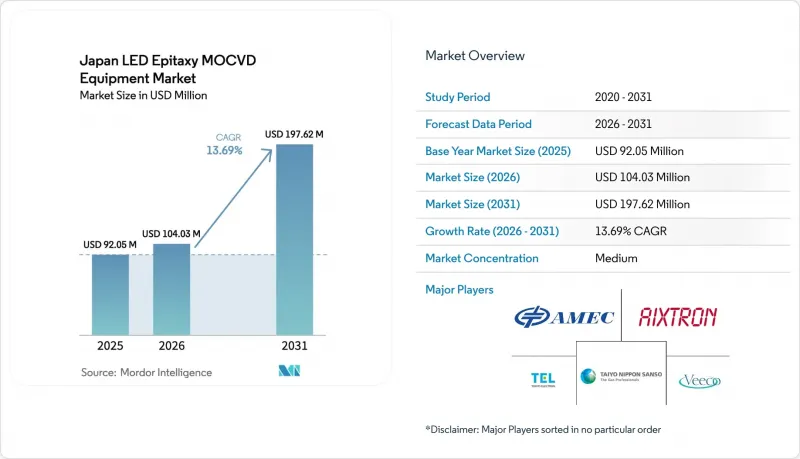
預計到 2025 年,日本用於 LED 外延的 MOCVD 設備市場規模將達到 9,205 萬美元,到 2026 年將達到 1.0403 億美元,到 2031 年將達到 1.9762 億美元,2026 年至 2031 年的複合年成長率為 13.3.39%。
此次擴張的驅動力包括政府補貼增加、對mini-LED和micro-LED的需求快速成長,以及GaN-on-Si功率元件晶圓尺寸向200mm和300mm的轉變。東京方面在2026會計年度推出的數十億美元半導體產業扶持計畫表明,日本國內設備製造商的訂單儲備充足。同時,原型開發的突破性成果,例如UV-C LED的牆壁插座效率達到10.2%,也證實了日本製造商已做好大規模生產下一代裝置的準備。此外,更大尺寸的晶圓降低了晶圓成本,而原位製程控制縮短了設備設定時間,這些都加速了老舊反應器的更換。儘管日圓匯率波動導致進口設備成本上升,但在企業淨零排放目標和旨在提高能源效率的維修的推動下,資本投資仍流向高效照明和電力電子領域。
日本LED外延MOCVD設備市場趨勢與洞察
迷你和微型LED背光需求激增
汽車駕駛座和旗艦消費電子產品對mini-LED和micro-LED背光的需求日益成長,這促使外延製程的公差越來越小,迫使供應商在150mm和200mm晶圓上實現亞奈米級的厚度控制。 Aixtron的G10-AsP平台實現了缺陷密度降低一個數量級,滿足了日本領先顯示器製造商對面板波長均勻性的要求,其面板解析度超過1000 ppi。包括Stanley Electric和京都大學光子晶體表面發射雷射計畫在內的本地研發夥伴關係表明,國內設備製造商能夠整合特定應用的製程配方。這些反應器的採購週期平均為六個月,使供應商能夠憑藉預先捆綁的測量技術和製程傳輸包獲得競爭優勢。總而言之,這些進步正在提高晶圓良率,縮短micro-LED模組的上市時間,並直接推動設備更新換代的需求。
政府對國內半導體製造設備的補貼
日本2026會計年度預算撥款1.23兆日圓(約79億美元)用於半導體和人工智慧領域,是上年度支援力度的四倍,為設備製造商提供可預測的多年訂單量。資本訂單將優先分配給區域產業叢集,包括台積電熊本工廠和Rapidus北海道項目,這兩個項目都致力於實現60%的設備和材料成本來自日本國內。津貼與技術里程碑掛鉤,降低了MOCVD設備閒置的風險。該政策也與加強出口管制相結合,透過將日本的供應從受限的中國需求轉向國內或盟國晶圓廠,保護供應商免受地緣政治波動的影響。
MOCVD設備與SiC外延替代技術的有限加工能力比較
與GaN MOCVD生產線相比,SiC CVD設備能夠以更高的速度沉積更厚的層,使功率半導體晶圓廠能夠提高單班晶圓加工量。 Ixtron將於2025年交付其第100台G10-SiC設備,顯示SiC設備在高壓領域可超越GaN。建模研究表明,GaN MOVPE的主要瓶頸在於氣相副產物的成核,這使得反應器設計變得複雜。因此,一些日本積體電路製造商(IDM)僅在電壓低於650V的裝置中使用GaN,這限制了對反應器的整體需求。
細分市場分析
氮化鎵(GaN)基LED外延系統在日本LED外延MOCVD設備市場佔據主導地位,預計2025年將佔69.09%的市佔率。這反映了其在白光照明、汽車頭燈和顯示器背光等領域的穩固地位。 GaN製程成熟度高、前驅體來源廣泛以及標準化的行星式反應器配方確保了其資本效率高,並能提供穩定的升級週期。儘管到2025年,AlGaN紫外線LED外延系統仍屬於小眾市場,但由於健康和安全法規的不斷完善以及水消毒項目的推進,其複合年成長率(CAGR)將達到14.65%。設備採購商優先考慮能夠抑制寄生鋁沉積的淋浴設備式反應器,這對於波長小於280奈米的發光元件至關重要。同時,對應變弛豫體InGaN的研究旨在取代紅色像素中的AlInGaP,進一步鞏固了對GaN族材料化學成分的投資。
此外,日本國內的整合舉措,例如羅姆公司計劃將台積電的氮化鎵(GaN)製程內部化,正有效鞏固其在氮化鎵LED外延MOCVD設備的市場佔有率。然而,紫外光刻供應商正面臨前驅體成本上漲和污染控制更加嚴格的困境,這提高了市場進入門檻。從長遠來看,結合MOCVD製程製備有源層和HVPE製程製備厚緩衝層的跨平台混合生產線可望降低單片成本,但目前的初步試驗結果僅限於4吋晶圓。
截至2025年,150mm晶圓相容設備佔據了日本LED外延MOCVD設備市場48.39%的佔有率。這是因為即使在中等產量下,傳統的藍寶石基GaN和矽基GaN生產線仍然盈利。然而,隨著IDM廠商追求晶圓成本降低,代工廠實現規模經濟效益,200mm及以上尺寸的系統正以14.38%的複合年成長率成長。 Propel300的汽車級650V GaN認證表明,其功率模組的缺陷率處於可接受水平,這意味著未來十年內300mm外延技術的全面應用是可能的。 imec等學術聯盟的試驗計畫已公佈了在300mm QST基板上超過800V的介電擊穿數據,進一步降低了這項轉型過程中的風險。
這種規模轉變絕非一帆風順。尺寸大於6英吋的獨立式GaN基板仍然稀缺,迫使許多LED製造商繼續使用150毫米藍寶石基板上的GaN。製程過渡還需要六個月的穩定期,在此期間良率的下降可能會抵消晶圓成本降低的好處。儘管如此,日本供應商正擴大採用自動化晶圓處理和人工智慧驅動的批次間控制技術,以縮短這個學習曲線。
其他好處:
- Excel格式的市場預測(ME)表
- 3個月的分析師支持
目錄
第1章:引言
- 研究假設和市場定義
- 調查範圍
第2章:調查方法
第3章執行摘要
第4章 市場狀況
- 市場概覽
- 市場促進因素
- 迷你型和微型LED背光燈需求激增
- 政府對國內半導體製造設備的補貼
- 擴大氮化鎵矽基功率元件的供應鏈
- 將汽車用UV-C LED應用於車載消毒領域。
- 功率IC IDM對150mm和200mm GaN晶圓的需求
- 各公司設定的淨零能耗目標正加速高效率照明的轉型。
- 市場限制因素
- MOCVD設備處理SiC外延替代方案的能力有其限制。
- 日圓疲軟,資本密集度高。
- 中國關鍵MOCVD組件供應鏈的集中度
- 日本汽車製造商的認證週期很長
- 產業供應鏈分析
- 技術展望
- 監理情勢
- 宏觀經濟因素對市場的影響
- 波特五力分析
- 新進入者的威脅
- 供應商的議價能力
- 買方的議價能力
- 替代品的威脅
- 競爭公司之間的競爭
第5章 市場規模與成長預測
- 按類別分類的LED材料系統
- 基於氮化鎵的LED外延系統
- AlGaN紫外線LED外延系統
- AlInGaP LED外延系統
- 晶圓尺寸特定功能
- 最大可達 100 毫米
- 150 mm
- 200毫米或以上
- 反應器配置
- 行星反應爐
- 淋浴設備噴頭式反應器
- 最終用戶
- LED整合製造商(IDM)
- 外延代工廠及外延專業供應商
第6章 競爭情勢
- 市場集中度
- 策略趨勢
- 市佔率分析
- 公司簡介
- Aixtron SE
- Veeco Instruments Inc.
- Advanced Micro-Fabrication Equipment Inc. China
- Beijing NAURA Microelectronics Equipment Co. Ltd.
- Taiyo Nippon Sanso Corporation
- Tokyo Electron Limited
- Kokusai Electric Corporation
- NuFlare Technology Inc.
- Kulicke and Soffa Industries Inc.
- Oxford Instruments plc
- Nichia Corporation
- Rohm Co. Ltd.
- Stanley Electric Co. Ltd.
- Toyoda Gosei Co. Ltd.
- Citizen Electronics Co. Ltd.
- Sharp Corporation
- Panasonic Holdings Corporation
- Sony Semiconductor Manufacturing Corporation
- Sumitomo Electric Industries, Ltd.
第7章 市場機會與未來展望
The Japan LED epitaxy MOCVD equipment marketsize is projected to be USD 92.05 million in 2025, USD 104.03 million in 2026, and reach USD 197.62 million by 2031, growing at a CAGR of 13.69% from 2026 to 2031.
An upswing in state subsidies, rapidly rising mini- and micro-LED demand, and the migration of GaN-on-Si power devices to 200 mm and 300 mm wafers underpin this expansion. Tokyo's multi-billion-dollar fiscal-2026 package for semiconductors signals predictable order pipelines for domestic toolmakers, while prototype breakthroughs such as a 10.2% wall-plug-efficiency UV-C LED confirm that Japan-based manufacturers are ready to scale next-generation devices. At the same time, larger wafer formats that lower die cost, and in-situ process control that shortens tool setup times, are sharpening replacement cycles for legacy reactors. Volatility in the yen does inflate imported tool costs, yet corporate net-zero mandates and energy-efficiency retrofits keep capital expenditure directed toward high-efficiency lighting and power electronics.
Japan LED Epitaxy MOCVD Equipment Market Trends and Insights
Surge in Mini and Micro-LED Backlighting Demand
Mini- and micro-LED backlighting for vehicle cockpits and flagship consumer electronics has tightened epitaxy tolerances, pushing suppliers toward sub-nanometer thickness control across 150 mm and 200 mm wafers. Aixtron's G10-AsP platform reports an order-of-magnitude reduction in defect density, aligning with Japan's display majors that require wavelength uniformity for panels exceeding 1,000 ppi. Local R&D partnerships, including Stanley Electric and Kyoto University's photonic-crystal surface-emitting laser program, demonstrate that domestic toolmakers can embed application-specific process recipes. Procurement cycles for these reactors average six months, rewarding vendors that pre-bundle metrology and process-transfer packages. Collectively, these developments raise per-wafer yields and shorten time-to-market for micro-LED modules, directly lifting equipment replacement demand.
Government Subsidies for Domestic Semiconductor Tools
Japan's fiscal-2026 budget allocates JPY 1.23 trillion (USD 7.9 billion) to semiconductors and AI, quadrupling prior-year support and providing predictable, multi-year order visibility for equipment makers. Capital grants flow first to regional clusters hosting TSMC's Kumamoto fab and Rapidus' Hokkaido project, both of which aim for 60% domestic procurement in tool and material spend. Subsidy tranches are linked to technical milestones, lowering the risk of stranded MOCVD assets. The policy also dovetails with tightened export controls that divert Japanese supply away from restricted Chinese demand and toward on-shore or allied fabs, cushioning suppliers against geopolitical swings.
Limited MOCVD Tool Throughput Versus SiC Epitaxy Alternatives
SiC CVD tools deposit thicker layers at higher rates, enabling power fabs to clear more wafers per shift than GaN MOCVD lines. Aixtron shipped its 100th G10-SiC tool in 2025, underscoring how SiC equipment can outpace GaN in high-voltage segments. Modeling studies reveal gas-phase by-product nucleation as a key bottleneck in GaN MOVPE, complicating reactor design. Consequently, several Japanese IDMs cherry-pick GaN only for sub-650 V devices, tempering total reactor demand.
Other drivers and restraints analyzed in the detailed report include:
- Expansion of GaN-on-Si Power Device Supply Chains
- Automotive UV-C LED Adoption for In-Cabin Sterilization
- High Capital Intensity Amid Yen Depreciation
For complete list of drivers and restraints, kindly check the Table Of Contents.
Segment Analysis
The GaN-based LED epitaxy systems segment dominated the Japan LED epitaxy MOCVD equipment market, accounting for 69.09% in 2025, reflecting its entrenched role in white lighting, automotive headlamps, and display backlights. Robust process maturity, broad precursor availability, and standardized planetary reactor recipes keep GaN capital efficient, ensuring stable upgrade cycles. AlGaN UV LED epitaxy systems, while niche in 2025, are tracking a 14.65% CAGR as health-safety regulations and water disinfection projects boost volumes. Equipment buyers value showerhead reactors that curb parasitic aluminum deposition, an essential attribute for sub-280 nm emitters. Concurrently, research into strain-relaxed bulk InGaN aims to displace AlInGaP in red pixels, which would further consolidate spend around GaN family chemistries.
The Japan LED epitaxy MOCVD equipment market share for GaN is also protected by domestic integration moves such as ROHM's plan to bring TSMC GaN recipes in-house. Yet UV suppliers confront higher precursor costs and stricter contamination control, raising barriers for new entrants. Long-term, cross-platform hybrid lines combining MOCVD for active layers with HVPE for thick buffers could cut per-wafer cost, but current pilot results remain limited to 4-inch experiments.
Tools configured for 150 mm wafers held 48.39% of the Japan LED epitaxy MOCVD equipment market share in 2025 because legacy GaN-on-sapphire and GaN-on-Si lines remain profitable at mid-volumes. However, 200 mm and larger systems are registering a 14.38% CAGR as IDMs chase lower die cost and foundries monetize scale economics. The Propel300's qualification for automotive-grade 650 V GaN validates defectivity levels acceptable for power modules, signaling that mass adoption of 300 mm epitaxy is plausible this decade. Pilot programs at academic consortia such as imec further de-risk this transition by publishing >800 V breakdown data on 300 mm QST substrates.
The scale shift is not friction-free. Free-standing GaN substrates above 6 inches remain scarce, compelling many LED makers to stay on 150 mm GaN-on-sapphire. Process migration also involves six-month stabilization windows, during which yield drag can offset wafer-cost gains. Even so, Japan's tool vendors increasingly bundle automated wafer handling and AI-driven run-to-run control that shorten this learning curve.
The Japan LED Epitaxy MOCVD Equipment Market Report is Segmented by LED Material System (GaN-Based LED Epitaxy Systems, and More), Wafer Size Capability (Up To 100mm, 150mm, and 200mm and Above), Reactor Configuration (Planetary Reactors, and Showerhead Reactors), End User (Integrated LED Manufacturers, and Epitaxy Foundries and Merchant Epi Suppliers). The Market Forecasts are Provided in Terms of Value (USD).
List of Companies Covered in this Report:
- Aixtron SE
- Veeco Instruments Inc.
- Advanced Micro-Fabrication Equipment Inc. China
- Beijing NAURA Microelectronics Equipment Co. Ltd.
- Taiyo Nippon Sanso Corporation
- Tokyo Electron Limited
- Kokusai Electric Corporation
- NuFlare Technology Inc.
- Kulicke and Soffa Industries Inc.
- Oxford Instruments plc
- Nichia Corporation
- Rohm Co. Ltd.
- Stanley Electric Co. Ltd.
- Toyoda Gosei Co. Ltd.
- Citizen Electronics Co. Ltd.
- Sharp Corporation
- Panasonic Holdings Corporation
- Sony Semiconductor Manufacturing Corporation
- Sumitomo Electric Industries, Ltd.
Additional Benefits:
- The market estimate (ME) sheet in Excel format
- 3 months of analyst support
TABLE OF CONTENTS
1 INTRODUCTION
- 1.1 Study Assumptions and Market Definition
- 1.2 Scope of the Study
2 RESEARCH METHODOLOGY
3 EXECUTIVE SUMMARY
4 MARKET LANDSCAPE
- 4.1 Market Overview
- 4.2 Market Drivers
- 4.2.1 Surge in Mini and Micro-LED Backlighting Demand
- 4.2.2 Government Subsidies for Domestic Semiconductor Tools
- 4.2.3 Expansion of GaN-on-Si Power Device Supply Chains
- 4.2.4 Automotive UV-C LED Adoption for In-Cabin Sterilization
- 4.2.5 Demand for 150 mm and 200 mm GaN Wafers from Power IC IDMs
- 4.2.6 Corporate Net-Zero Targets Accelerating High-Efficiency Lighting Retrofits
- 4.3 Market Restraints
- 4.3.1 Limited MOCVD Tool Throughput Versus SiC Epitaxy Alternatives
- 4.3.2 High Capital Intensity Amid Yen Depreciation
- 4.3.3 Supply Chain Concentration in China for Key MOCVD Components
- 4.3.4 Slow Qualification Cycles at Japanese Automotive OEMs
- 4.4 Industry Supply Chain Analysis
- 4.5 Technological Outlook
- 4.6 Regulatory Landscape
- 4.7 Impact of Macroeconomic Factors on the Market
- 4.8 Porter's Five Forces Analysis
- 4.8.1 Threat of New Entrants
- 4.8.2 Bargaining Power of Suppliers
- 4.8.3 Bargaining Power of Buyers
- 4.8.4 Threat of Substitutes
- 4.8.5 Intensity of Competitive Rivalry
5 MARKET SIZE AND GROWTH FORECASTS (VALUE)
- 5.1 By LED Material System
- 5.1.1 GaN-based LED Epitaxy Systems
- 5.1.2 AlGaN UV LED Epitaxy Systems
- 5.1.3 AlInGaP LED Epitaxy Systems
- 5.2 By Wafer Size Capability
- 5.2.1 Upto 100 mm
- 5.2.2 150 mm
- 5.2.3 200 mm and Above
- 5.3 By Reactor Configuration
- 5.3.1 Planetary Reactors
- 5.3.2 Showerhead Reactors
- 5.4 By End User
- 5.4.1 Integrated LED Manufacturers (IDMs)
- 5.4.2 Epitaxy Foundries and Merchant Epi Suppliers
6 COMPETITIVE LANDSCAPE
- 6.1 Market Concentration
- 6.2 Strategic Moves
- 6.3 Market Share Analysis
- 6.4 Company Profiles (Includes Global Level Overview, Market Level Overview, Core Segments, Financials as Available, Strategic Information, Market Rank/Share, Products and Services, and Recent Developments)
- 6.4.1 Aixtron SE
- 6.4.2 Veeco Instruments Inc.
- 6.4.3 Advanced Micro-Fabrication Equipment Inc. China
- 6.4.4 Beijing NAURA Microelectronics Equipment Co. Ltd.
- 6.4.5 Taiyo Nippon Sanso Corporation
- 6.4.6 Tokyo Electron Limited
- 6.4.7 Kokusai Electric Corporation
- 6.4.8 NuFlare Technology Inc.
- 6.4.9 Kulicke and Soffa Industries Inc.
- 6.4.10 Oxford Instruments plc
- 6.4.11 Nichia Corporation
- 6.4.12 Rohm Co. Ltd.
- 6.4.13 Stanley Electric Co. Ltd.
- 6.4.14 Toyoda Gosei Co. Ltd.
- 6.4.15 Citizen Electronics Co. Ltd.
- 6.4.16 Sharp Corporation
- 6.4.17 Panasonic Holdings Corporation
- 6.4.18 Sony Semiconductor Manufacturing Corporation
- 6.4.19 Sumitomo Electric Industries, Ltd.
7 MARKET OPPORTUNITIES AND FUTURE OUTLOOK
- 7.1 White-space and Unmet-Need Assessment
 化學氣相沉積 (CVD) 市場規模、佔有率和趨勢分析報告:按類別、應用、地區和細分市場分類 - 預測 (2026–2033)
 化學氣相沉積設備市場報告:按技術、應用、最終用戶和地區分類(2026-2034 年)
 LED外延MOCVD設備:市場佔有率分析、產業趨勢與統計、成長預測(2026-2031年)中國LED外延MOCVD設備:市佔率分析、產業趨勢與統計及成長預測(2026-2031年)亞太地區LED外延MOCVD設備:市場佔有率分析、產業趨勢與統計及成長預測(2026-2031年)
 化學氣相沉積(CVD)市場:按技術類型、材料、前驅體類型、應用和最終用途產業分類-2026-2032年全球市場預測
 2026年全球異質接面(HJT)等離子體增強化學氣相沉積(PECVD)設備市場報告2026年全球等離子體增強化學蒸氣沉積(PECVD)設備市場報告
 半導體化學氣相沉積設備市場:依產品類型、應用、國家及地區分類-全球產業分析、市場規模、市場佔有率及2026年至2033年預測半導體薄膜沉積設備市場:按材料、設備、技術、產業、終端用戶應用、國家和地區分類-全球產業分析、市場規模、市場佔有率和預測(2026-2033 年)