


 |
市場調查報告書
商品編碼
2044043
亞太地區LED外延MOCVD設備:市場佔有率分析、產業趨勢與統計及成長預測(2026-2031年)Asia-Pacific LED Epitaxy MOCVD Equipment - Market Share Analysis, Industry Trends & Statistics, Growth Forecasts (2026 - 2031) |
||||||
※ 本網頁內容可能與最新版本有所差異。詳細情況請與我們聯繫。
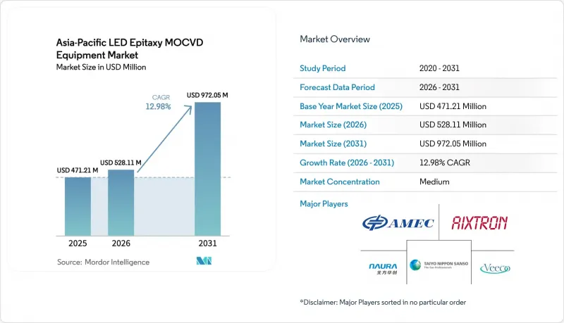
預計亞太地區用於 LED 外延的 MOCVD 設備市場規模將在 2025 年達到 4.7121 億美元,2026 年達到 5.2811 億美元,2031 年達到 9.7205 億美元,2026 年至 2031 年的複合年成長率為 12.98%。
政府對國內半導體製造設備的大力支持、向Mini-LED和Micro-LED顯示器的轉型以及更大尺寸GaN晶圓的普及,共同推動了中國大陸、台灣、日本和韓國的資本投資加速成長。本地供應商正積極響應北京關於至少一半新半導體製造設備必須從國內供應商採購的指令,而顯示器製造商則在對先進的淋浴設備反應器進行認證,以滿足嚴格的波長分檔目標。鎵出口限制正在增強區域自給自足能力,促進長期供應鏈重組,並擴大對國產前驅體純化的潛在需求。同時,人工智慧驅動的原位測量技術正成為新系統的標配,從而降低缺陷密度並縮短根本原因分析週期。此外,翻新計畫使二線晶圓廠能夠利用成熟的反應器,在無需大規模資本投資的情況下逐步提升產能。
亞太地區LED外延MOCVD設備市場的趨勢與洞察。
中國政府對化合物半導體製造的補貼
中國「大基金三期」累計475億美元,旨在加速引進國產設備,並設定配額,要求新購設備的一半必須來自國產供應商。預計國產設備在國內市場的滲透率將從2024年的25%提升至2025年的35%,將直接促進諾瑞科技集團和先進微加工設備股份有限公司的出貨量成長。省級稅收優惠和產業園區補貼政策已使晶圓廠的實際資本投資減少了高達30%,從而帶動了多晶圓反應器訂單的增加。鎵資源的優勢進一步推動了國家獎勵與供應鏈本地化進程的契合。鄰國馬來西亞和越南的LED製造商已開始從中國採購生產設備,以利用稅收優惠的貿易通道,這進一步放大了這一因素的區域連鎖效應。
Mini-LED 和 Micro-LED 顯示器需求激增
Omdia預測,2025年至2026年間,全球microLED顯示器銷售額將翻倍,到2032年達到68億美元。 2024年,Mini-LED電視出貨量達到820萬台,較去年同期成長100%,推動了對窄通道外延晶圓的需求。顯示器供應商目前要求波長公差為±2.5奈米,促使製程從行星式反應器轉向淋浴設備反應器。 Veeco的Lumina系列產品已獲得2026年用於AI伺服器光鏈路的磷化銦雷射的持續訂單,凸顯了跨市場協同效應。雖然板載晶片(COB)背光面臨供應過剩的風險,但其在汽車儀錶板和擴增實境(AR)頭顯中的應用正在吸收閒置的外延產能。
多晶圓MOCVD設備的高昂資本投資成本
最先進的200毫米批式反應器售價在300萬至500萬美元之間,對年銷售額低於5000萬美元的晶圓廠來說是一道障礙。 Alliance MOCVD和Heraeus Covantix提供翻新100毫米設備的30%至40%折扣,但二手市場上全新的150毫米或200毫米設備的供應有限。 4至6年的漫長投資回收期阻礙了新的投資,尤其是在需求前景不明朗的情況下。雖然租賃安排在台灣和日本越來越普遍,但中國當地的金融機構仍然保持謹慎,限制了資金籌措。因此,資本投資的負擔正在減緩技術轉型,並抑制亞太地區LED外延MOCVD設備市場短期出貨量的激增。
細分市場分析
氮化鎵(GaN)平台憑藉其在通用照明、背光和汽車頭燈等領域的成熟應用,預計到2025年將佔68.86%的市場佔有率。成熟的前驅體生態系統和豐富的基板選擇確保了GaN晶片的成本競爭力,鞏固了其在亞太地區LED外延MOCVD設備市場的主導地位。台積電(TSMC)20億美元的鎵回收計畫進一步保障了GaN供應免受出口波動的影響。儘管AlGaN UV-C裝置的基準較小,但在水處理和醫療設施嚴格的衛生標準的推動下,其預計複合年成長率仍將達到13.24%。歐洲和北美嚴格的排放法規已推動市政維修項目,從而帶動了能夠維持1100 度C以上生長窗口的高溫反應器設備的強勁訂單。
供應鏈專業化正在推進。中國大陸和台灣的晶圓代工廠正利用人工智慧驅動的洞察測量技術來解決高密度位錯問題,並擴大AlGaN外延中試生產線的產能。同時,歐美供應商正將藍圖從砷化物基磷反應器轉向電力電子和太陽能聚光器市場,這使得亞太地區的本土企業能夠鞏固其GaN LED市場佔有率。因此,在亞太地區的LED外延MOCVD設備產業,GaN預計仍將是主要的收入來源,而AlGaN有望成為成長的驅動力,並透過協同效應提高利潤率。
預計到2025年,150mm晶圓市佔率將達到46.39%,反映了其在LED量產製造領域長期佔據的重要地位。然而,200mm及以上晶圓市場預計將實現13.63%的複合年成長率,因為更大的基板能夠降低單晶片成本,並與主流矽晶圓廠的物流系統相契合。運轉率的提高歸功於邊緣排除區的減少,該區域在100mm晶圓中佔比接近20%,而在200mm晶圓中已降至約8-10%,從而提高了每平方厘米的有效資本效率。 Veeco的Propel平台能夠實現向300mm晶圓的無縫過渡,這體現了設備製造商致力於幫助客戶規劃未來發展藍圖的努力。
然而,這種轉型並不均衡。日本和台灣的積體電路製造商(IDM)透過改造現有的DRAM潔淨室用於GaN外延,最大限度地減少了額外的基礎設施投資;而中國當地的許多晶圓廠則需要資金籌措安裝全新的氣體和廢氣處理系統,以適應200mm晶圓。由於藍寶石的成本和缺陷率,一些UV-C和雷射應用目前僅限於150mm晶圓,這有助於維持多尺寸生態系統。整體而言,這種轉型趨勢凸顯了晶圓尺寸的變化如何影響亞太地區LED外延MOCVD設備市場的資本投資時機。
其他好處:
- Excel格式的市場預測(ME)表
- 3個月的分析師支持
目錄
第1章:引言
- 研究假設和市場定義
- 調查範圍
第2章:調查方法
第3章執行摘要
第4章 市場狀況
- 市場概覽
- 市場促進因素
- 中國政府對化合物半導體製造的補貼
- Mini-LED 和 Micro-LED 顯示器需求激增
- 過渡到 150 毫米和 200 毫米 GaN 晶圓以降低成本。
- UV-C LED消毒系統的應用日益普及
- 透過整合人工智慧驅動的現場測量技術來減少產量損失。
- 透過對圓形反應器維修,減少資本支出(CapEx)。
- 市場限制因素
- 多晶圓MOCVD設備的高額購買成本
- LED背光市場供應過剩風險
- 三甲基鎵和氨的供應鏈不穩定
- 二線城市缺乏經驗豐富的外延技術人員
- 產業供應鏈分析
- 技術展望
- 監理情勢
- 宏觀經濟因素對市場的影響
- 波特五力分析
- 新進入者的威脅
- 供應商的議價能力
- 買方的議價能力
- 替代品的威脅
- 競爭公司之間的競爭
第5章 市場規模與成長預測
- 按類別分類的LED材料系統
- 基於氮化鎵的LED外延系統
- AlGaN紫外線LED外延系統
- AlInGaP LED外延系統
- 按晶圓尺寸
- 最大可達 100 毫米
- 150 mm
- 200毫米或以上
- 反應器配置
- 行星反應爐
- 淋浴設備噴頭式反應器
- 最終用戶
- LED整合製造商(IDM)
- 外延代工廠及外延專業供應商
- 國家
- 中國
- 日本
- 台灣
- 亞太其他地區
第6章 競爭情勢
- 市場集中度
- 策略趨勢
- 市佔率分析
- 公司簡介
- AIXTRON SE
- Veeco Instruments Inc.
- Advanced Micro-Fabrication Equipment Inc.(AMEC)
- NAURA Technology Group Co. Ltd.
- Taiyo Nippon Sanso Corporation
- ASM International NV
- Tokyo Electron Ltd.
- Applied Materials Inc.
- topecsh Co. Ltd.
- CVD Equipment Corporation
- NuFlare Technology Inc.
- Jusung Engineering Co. Ltd.
- Element 3-5 GmbH
- Alliance MOCVD LLC
- Suzhou Powerway Wafer Co. Ltd.
- Sanan Optoelectronics Co. Ltd.
- Epistar Corporation
- Silan Azure Co. Ltd.
第7章 市場機會與未來展望
The Asia-Pacific LED epitaxy MOCVD equipment market size is projected to be USD 471.21 million in 2025, USD 528.11 million in 2026, and reach USD 972.05 million by 2031, growing at a CAGR of 12.98% from 2026 to 2031.
Robust state incentives for domestic semiconductor tools, the pivot toward mini-LED and micro-LED displays, and the shift to larger GaN wafers are together accelerating capital spending across China, Taiwan, Japan, and South Korea. Local equipment vendors are capitalizing on Beijing's mandate that at least half of new semiconductor tools come from domestic suppliers, while display makers are qualifying advanced showerhead reactors to meet tight wavelength-binning targets. Gallium export controls are reinforcing regional self-reliance, driving long-term supply-chain realignment, and expanding addressable demand for indigenous precursor purification. At the same time, AI-driven in-situ metrology is becoming standard on new tools, cutting defect density and shortening root-cause analysis cycles. Refurbishment programs are widening access to mature reactors for Tier-2 fabs, enabling incremental capacity additions without full capital outlays.
Asia-Pacific LED Epitaxy MOCVD Equipment Market Trends and Insights
Government Subsidies for Compound-Semiconductor Fabs in China
China's Big Fund Phase 3 set aside USD 47.5 billion to accelerate domestic tool adoption, with quotas stipulating that half of new equipment purchases come from local vendors. Domestic penetration rose from 25% in 2024 to 35% in 2025, directly lifting shipments for NAURA Technology Group and Advanced Micro-Fabrication Equipment Inc. Provincial tax holidays and subsidized industrial parks have cut effective fab capex by up to 30%, unlocking incremental orders for multi-wafer reactors. Gallium resource dominance further aligns state incentives with supply-chain localization. Neighboring Malaysian and Vietnamese LED makers are already sourcing Chinese tools to qualify for reduced-tariff trade corridors, reinforcing the driver's regional spill-over effect.
Surge in Demand for Mini and Micro-LED Displays
Omdia projects global micro-LED display revenue to double between 2025 and 2026, then scale to USD 6.8 billion by 2032. Mini-LED TV shipments climbed 100% year-over-year to 8.2 million units in 2024, lifting demand for narrow-binning epitaxial wafers. Display suppliers now require +-2.5 nm wavelength tolerance, prompting migration from planetary to showerhead reactors. Veeco's Lumina series logged repeat orders in 2026 for indium-phosphide lasers that support AI-server optical links, highlighting cross-market synergies. Although chip-on-board backlighting faces oversupply risk, adoption in automotive dashboards and augmented-reality headsets is absorbing idle epi capacity.
High Capital Cost of Multi-Wafer MOCVD Tools
State-of-the-art 200 mm batch reactors carry USD 3-5 million price tags, a hurdle for fabs with annual sales below USD 50 million. Although Alliance MOCVD and Heraeus Covantics offer 30-40% discounts on refurbished 100 mm equipment, availability of newer 150 mm or 200 mm tools in the secondary market is limited. Long four-to-six-year payback periods discourage greenfield investment when demand visibility narrows. Leasing structures are emerging in Taiwan and Japan, yet mainland China lenders remain cautious, keeping financing channels constrained. The capex burden therefore delays technology transitions and tempers short-term shipment spikes for the Asia-Pacific LED epitaxy MOCVD equipment market.
Other drivers and restraints analyzed in the detailed report include:
- Shift to 150 mm and 200 mm GaN Wafers for Cost Reduction
- Increasing Adoption of UV-C LED Disinfection Systems
- Oversupply Risk in LED Backlighting Market
For complete list of drivers and restraints, kindly check the Table Of Contents.
Segment Analysis
GaN platforms anchored 68.86% of the market share in 2025, thanks to entrenched use in general lighting, backlighting, and automotive headlamps. Mature precursor ecosystems and substrate optionality keep GaN die costs competitive, reinforcing the Asia-Pacific LED epitaxy MOCVD equipment market's installed base advantage. Taiwan Semiconductor Manufacturing Company's USD 2 billion gallium recycling program is further insulating GaN supply from export volatility. AlGaN UV-C devices sit at a smaller baseline yet carry a 13.24% forecast CAGR, buoyed by stringent hygiene mandates in water-treatment and healthcare facilities. Tight emission regulations in Europe and North America are already spurring municipal retrofit projects, translating into firm tool orders for high-temperature reactors that can sustain >1,100 °C growth windows.
Supply-chain specialization is deepening. Chinese and Taiwanese foundries are ramping AlGaN epi pilot lines, leveraging AI-driven in-situ metrology to tackle high threading-dislocation density. Western vendors, meanwhile, are redirecting arsenide-phosphide reactor roadmaps toward power electronics and solar concentrator markets, allowing domestic APAC players to consolidate GaN LED share. The Asia-Pacific LED epitaxy MOCVD equipment industry therefore expects GaN to remain the revenue anchor, while AlGaN provides the incremental growth zest that lifts blended margins.
In 2025, the 150 mm segment accounted for 46.39% of the market share, reflecting its long-standing role in volume LED manufacturing. Yet the 200 mm and above category is charted to post a 13.63% CAGR, as larger substrates lower per-die cost and align with mainstream silicon fab logistics. Utilization improvements stem from smaller edge exclusion zones, which drop from near 20% on 100 mm wafers to roughly 8-10% on 200 mm lots, enhancing effective capital-per-square-centimeter economics. Veeco's Propel platform, capable of seamless 300 mm transitions, illustrates equipment makers' push to future-proof customer roadmaps.
The transition, however, is uneven. Japanese and Taiwanese IDMs have re-purposed legacy DRAM cleanrooms for GaN epi, minimizing incremental infrastructure spend, whereas many mainland Chinese fabs must finance entirely new bulk-gas and abatement systems for 200 mm readiness. Sapphire cost and defectivity currently limit some UV-C and laser applications to 150 mm, preserving a multi-diameter ecosystem. Overall, migration dynamics underscore how wafer-size shifts can swing capex timing for the Asia-Pacific LED epitaxy MOCVD equipment market.
The Asia-Pacific LED Epitaxy MOCVD Equipment Market Report is Segmented by LED Material System (GaN-Based LED Epitaxy Systems, and More), Wafer Size Capability (Up To 100mm, 150mm, and 200mm and Above), Reactor Configuration (Planetary Reactors, and Showerhead Reactors), End User (Integrated LED Manufacturers, and Epitaxy Foundries and Merchant Epi Suppliers), and Country. The Market Forecasts are Provided in Terms of Value (USD).
List of Companies Covered in this Report:
- AIXTRON SE
- Veeco Instruments Inc.
- Advanced Micro-Fabrication Equipment Inc. (AMEC)
- NAURA Technology Group Co. Ltd.
- Taiyo Nippon Sanso Corporation
- ASM International N.V.
- Tokyo Electron Ltd.
- Applied Materials Inc.
- topecsh Co. Ltd.
- CVD Equipment Corporation
- NuFlare Technology Inc.
- Jusung Engineering Co. Ltd.
- Element 3-5 GmbH
- Alliance MOCVD LLC
- Suzhou Powerway Wafer Co. Ltd.
- Sanan Optoelectronics Co. Ltd.
- Epistar Corporation
- Silan Azure Co. Ltd.
Additional Benefits:
- The market estimate (ME) sheet in Excel format
- 3 months of analyst support
TABLE OF CONTENTS
1 INTRODUCTION
- 1.1 Study Assumptions and Market Definition
- 1.2 Scope of the Study
2 RESEARCH METHODOLOGY
3 EXECUTIVE SUMMARY
4 MARKET LANDSCAPE
- 4.1 Market Overview
- 4.2 Market Drivers
- 4.2.1 Government Subsidies for Compound-Semiconductor Fabs in China
- 4.2.2 Surge in Demand for Mini and Micro-LED Displays
- 4.2.3 Shift to 150 mm and 200 mm GaN Wafers for Cost Reduction
- 4.2.4 Increasing Adoption of UV-C LED Disinfection Systems
- 4.2.5 AI-Driven In-Situ Metrology Integration Reducing Yield Loss
- 4.2.6 Circular Reactor Refurbishment Programs Lowering CapEx
- 4.3 Market Restraints
- 4.3.1 High Capital Cost of Multi-Wafer MOCVD Tools
- 4.3.2 Oversupply Risk in LED Backlighting Market
- 4.3.3 Volatile Trimethylgallium and Ammonia Supply Chains
- 4.3.4 Shortage of Experienced Epitaxy Engineers in Tier-2 Cities
- 4.4 Industry Supply Chain Analysis
- 4.5 Technological Outlook
- 4.6 Regulatory Landscape
- 4.7 Impact of Macroeconomic Factors on the Market
- 4.8 Porter's Five Forces Analysis
- 4.8.1 Threat of New Entrants
- 4.8.2 Bargaining Power of Suppliers
- 4.8.3 Bargaining Power of Buyers
- 4.8.4 Threat of Substitutes
- 4.8.5 Intensity of Competitive Rivalry
5 MARKET SIZE AND GROWTH FORECASTS (VALUE)
- 5.1 By LED Material System
- 5.1.1 GaN-based LED Epitaxy Systems
- 5.1.2 AlGaN UV LED Epitaxy Systems
- 5.1.3 AlInGaP LED Epitaxy Systems
- 5.2 By Wafer Size Capability
- 5.2.1 Upto 100 mm
- 5.2.2 150 mm
- 5.2.3 200 mm and Above
- 5.3 By Reactor Configuration
- 5.3.1 Planetary Reactors
- 5.3.2 Showerhead Reactors
- 5.4 By End User
- 5.4.1 Integrated LED Manufacturers (IDMs)
- 5.4.2 Epitaxy Foundries and Merchant Epi Suppliers
- 5.5 By Country
- 5.5.1 China
- 5.5.2 Japan
- 5.5.3 Taiwan
- 5.5.4 Rest of Asia-Pacific
6 COMPETITIVE LANDSCAPE
- 6.1 Market Concentration
- 6.2 Strategic Moves
- 6.3 Market Share Analysis
- 6.4 Company Profiles (Includes Global Level Overview, Market Level Overview, Core Segments, Financials as Available, Strategic Information, Market Rank/Share, Products and Services, and Recent Developments)
- 6.4.1 AIXTRON SE
- 6.4.2 Veeco Instruments Inc.
- 6.4.3 Advanced Micro-Fabrication Equipment Inc. (AMEC)
- 6.4.4 NAURA Technology Group Co. Ltd.
- 6.4.5 Taiyo Nippon Sanso Corporation
- 6.4.6 ASM International N.V.
- 6.4.7 Tokyo Electron Ltd.
- 6.4.8 Applied Materials Inc.
- 6.4.9 topecsh Co. Ltd.
- 6.4.10 CVD Equipment Corporation
- 6.4.11 NuFlare Technology Inc.
- 6.4.12 Jusung Engineering Co. Ltd.
- 6.4.13 Element 3-5 GmbH
- 6.4.14 Alliance MOCVD LLC
- 6.4.15 Suzhou Powerway Wafer Co. Ltd.
- 6.4.16 Sanan Optoelectronics Co. Ltd.
- 6.4.17 Epistar Corporation
- 6.4.18 Silan Azure Co. Ltd.
7 MARKET OPPORTUNITIES AND FUTURE OUTLOOK
- 7.1 White-Space and Unmet-Need Assessment
 化學氣相沉積 (CVD) 市場規模、佔有率和趨勢分析報告:按類別、應用、地區和細分市場分類 - 預測 (2026–2033)
 化學氣相沉積設備市場報告:按技術、應用、最終用戶和地區分類(2026-2034 年)
 LED外延MOCVD設備:市場佔有率分析、產業趨勢與統計、成長預測(2026-2031年)中國LED外延MOCVD設備:市佔率分析、產業趨勢與統計及成長預測(2026-2031年)日本LED外延MOCVD設備:市佔率分析、產業趨勢與統計及成長預測(2026-2031年)
 化學氣相沉積(CVD)市場:按技術類型、材料、前驅體類型、應用和最終用途產業分類-2026-2032年全球市場預測
 2026年全球異質接面(HJT)等離子體增強化學氣相沉積(PECVD)設備市場報告2026年全球等離子體增強化學蒸氣沉積(PECVD)設備市場報告
 半導體化學氣相沉積設備市場:依產品類型、應用、國家及地區分類-全球產業分析、市場規模、市場佔有率及2026年至2033年預測半導體薄膜沉積設備市場:按材料、設備、技術、產業、終端用戶應用、國家和地區分類-全球產業分析、市場規模、市場佔有率和預測(2026-2033 年)