


 |
市場調查報告書
商品編碼
2044042
LED外延MOCVD設備:市場佔有率分析、產業趨勢與統計、成長預測(2026-2031年)LED Epitaxy MOCVD Equipment - Market Share Analysis, Industry Trends & Statistics, Growth Forecasts (2026 - 2031) |
||||||
※ 本網頁內容可能與最新版本有所差異。詳細情況請與我們聯繫。
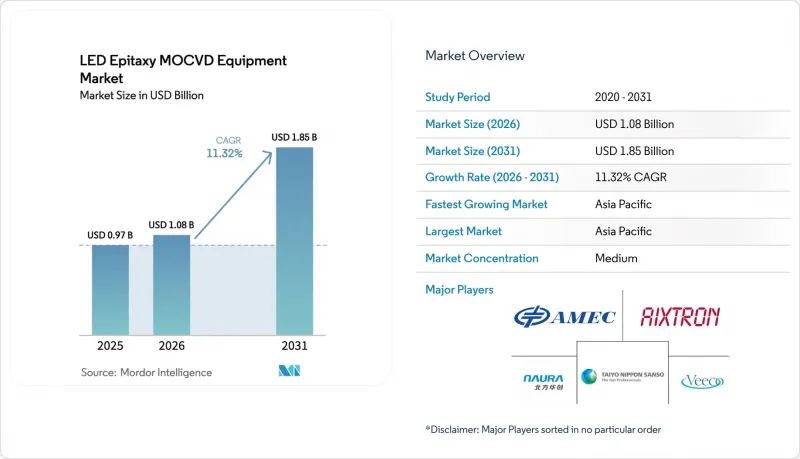
LED外延MOCVD設備的市場規模預計將從2025年的9.7億美元成長到2026年的10.8億美元,然後從2026年到2031年以11.32%的複合年成長率成長,到2031年達到18.5億美元。
顯示器製造商正從側光式LCD背光轉向直下式mini-LED和micro-LED架構,這增加了每台電視和儀錶板對晶圓的需求。化合物半導體晶圓廠正轉向200mm GaN-on-Si基板,這種基板可與功率電子裝置共用設備,從而降低成本並提高進入門檻。來自美國《晶片與科學法案》、歐盟《晶片法案》以及中國多個省級基金的補貼計畫正在推動國內新型外延產能的擴張。 LED外延MOCVD設備市場的發展趨勢與更廣泛的晶圓製造設備週期有所不同。這是因為,即使記憶體和邏輯電路的投資暫時停滯,諸如消毒、汽車安全和能源效率等監管因素仍然支撐著需求。
全球LED外延MOCVD設備市場趨勢及洞察
迷你LED和微型LED背光技術的普及
面板製造商正以直下式mini-LED和micro-LED矩陣取代側光式組件,使每台電視能夠實現超過10,000個調光區域。每款高階機種使用的外延晶圓面積是先前傳統背光的10倍,從而提高了反應器的穩定運轉率。 micro-LED正被應用於汽車儀錶板、抬頭顯示器和擴增實境(AR)穿戴式設備,以確保在陽光下的可視性,進一步擴大了目標市場規模。三安光電在通過客戶審核後表示,micro-LED將於2025年實現商業化規模,其micro-LED產能已提升至每月1,400片6吋晶圓以上。代工廠指出,超大規模資料中心對支援光連接模組的藍色和綠色晶片的需求不斷成長,這為顯示器以外的成長領域提供了新的發展空間。剩下的瓶頸是GaN-on-Si中的高效紅色發射,為此,供應商正在努力改進腔室設計,以便在不發生交叉污染的情況下切換到AlInGaP製程。
加速向 200 毫米 GaN-on-Si 平台過渡
LED製造商正積極尋求200mm GaN-on-Si模板的認證,以便與功率裝置生產線分攤折舊免稅額成本,並將每晶片的外延成本降低約三分之一。 Ennostar和ALLOS Semiconductors正在共同開發一種通用基板,使其能夠在同一反應器陣列中同時生產頭燈LED和650V電晶體。 IQE已在英國紐波特和美國馬薩諸塞州部署了多晶圓設備,展示了在同一腔室中生長汽車級功率裝置和微型LED晶圓的能力。由於控制200mm晶圓的彎曲仍然是一項挑戰,因此具有多區域加熱和即時溫度測量功能的行星式反應器價格昂貴。平均運轉率超過70%後,晶圓廠業主報告稱,與150mm生產線相比,每流明成本降低了30%,這正在推動2027年後的第二波轉型浪潮。
一般照明投資的週期性
儘管通用照明仍佔晶圓產量的約40%,但由於建築週期、補貼計畫結束以及利率波動等因素,終端市場需求波動較大。三安光電2025年的利潤率有所提高,但其LED晶圓銷量較去年同期下降約4%。這表明製造商已將產能轉移到汽車和顯示器等細分市場。根據愛思創提交的文件,由於客戶推遲訂單以調整庫存,其LED業務的市場佔有率在2025年出現了兩位數的萎縮。隨著燈具壽命超過5萬小時,更換需求正在放緩,成長軸心正在轉向智慧照明維修,但這一趨勢在景氣衰退時期也會停滯。因此,如果住宅量和商業租賃需求下降,預計LED外延MOCVD設備市場將在短期內停滯。
細分市場分析
作為通用照明和汽車燈具用藍光和白光二極體的基礎,GaN平台在2025年仍佔LED外延MOCVD設備市場67.86%的佔有率。儘管AlGaN紫外線設備規模較小,但預計到2031年將以12.53%的複合年成長率成長,這主要得益於汞基滅菌設備的逐步淘汰,使其成為所有材料體系中成長最快的。雖然與可見光頻譜的產能相比,用於AlGaN生產線的LED外延MOCVD設備的市場規模仍然小規模,但每個已安裝的反應器都能生產出平均售價較高的晶圓,從而為供應商帶來可觀的毛利率。近期向歐洲大學的供貨反映了公共衛生資金籌措的強勁成長勢頭,也抵消了製程初期階段的複雜性。
當鋁含量超過50%時,大多數製造商都會面臨效率下降的問題,這促使人們致力於脈衝前驅體供給技術的研究,以減少位錯的形成、原位應力監測以及基板切割誤差。 IQE公司正在推行雙管齊下的策略:一方面利用GaAs維持紅色發光,另一方面開發下一代氮化鎵替代方案。設備製造商正在透過混合腔室來解決這個問題,這種腔室可以在一次預防性保養週期內切換GaN、AlGaN和AlInGaP三種材料,為必須滿足多色microLED客戶需求的代工廠節省高達30%的資本支出。
到2025年,在完善的製程和現有晶圓廠基礎設施的支援下,相容150毫米晶圓的反應器將佔據47.39%的市場佔有率。預計到2031年,與200毫米設備相關的LED外延MOCVD設備的市場規模將以12.38%的複合年成長率快速成長,這主要得益於整合裝置製造商(IDM)對暫停中矽生產線的維修以及對規模經濟的追求。儘管翹曲控制方面仍存在挑戰,但採用區域加熱的行星式反應器已實現超過85%的良率,正在縮小與小尺寸晶圓的差距。
晶圓代工廠正利用這種更大的尺寸規格,與下游針對功率元件最佳化的切割和封裝生產線相匹配,從而顯著降低每流明成本。普華永道指出,光電子裝置在直徑轉型方面落後於邏輯裝置。然而,200毫米的轉捩點出現在單一設備的年產量超過1萬片時。擁有大量汽車產品且制定了微型LED發展藍圖裝置製造商(IDM)已經超過了這一產量,但通用燈具供應商仍依賴已完全折舊免稅額的100毫米和150毫米設備。
區域分析
預計到2025年,亞太地區將佔LED外延MOCVD設備市場收入的48.42%,並在2031年之前以12.98%的複合年成長率成長。中國地方政府和國家基金累計總合8.4億美元用於化合物半導體的自給自足,為設備購買和前驅體工廠建設提供補貼。在台灣,傳統的100mm生產線正在向150mm和200mm規格過渡,在不新建設的情況下擴大了產能。三安光電在獲得三星認證後,提高了其6吋microLED的產能,顯示其生態系已具備大規模生產顯示級LED的條件。在日本和韓國,日亞化學工業株式會社和首爾半導體正在升級設備以滿足更高發光效率的要求,並保持強勁的升級需求。
預計到2025年,北美和歐洲的市佔率總合將達到35%至40%左右,而產量成長的驅動力並非燈具銷售,而是補貼計畫的實施。美國政府向IntelliEPI、Coherent、Macom和GlobalWafers等公司提供了數百萬美元的津貼,鼓勵它們在國內進行晶圓生產。布魯塞爾方面向IMEC的試點生產線注資7億歐元(約7.56億美元),旨在將其對進口氮化矽晶圓的依賴度降低一半。出口許可證的申請延長了銷往中國的高性能反應器的前置作業時間,促使歐美供應商優先將有限的產能分配給中國客戶,導致中國國內訂單積壓增加。
包括南美、中東和非洲在內的「世界其他地區」預計在2025年將佔全球銷售額的十分之一左右。澳洲將於2026年3月設立140流明/瓦的最低標準,將間接提高晶圓品質要求,並刺激高均勻性晶片的進口。海灣國家的市政當局正在將自適應路燈納入其智慧城市計劃,但晶片供應商仍主要來自韓國和中國。太陽能UV-C模組正在非洲農村地區的用水和污水和衛生試點計畫中得到應用,這形成了小規模但具有戰略意義的需求區域,而與亞洲公司有關聯的外延片製造商正在積極滿足這一需求。
其他好處:
- Excel格式的市場預測(ME)表
- 3個月的分析師支持
目錄
第1章:引言
- 研究假設和市場定義
- 調查範圍
第2章:調查方法
第3章執行摘要
第4章 市場狀況
- 市場概覽
- 市場促進因素
- 迷你LED和微型LED背光技術的普及
- 加速向 200 毫米 GaN-on-Si 平台過渡
- 對UV-C LED消毒系統的需求正在擴大。
- 政府對化合物半導體製造的補貼
- 汽車原始設備製造商向自我調整LED頭燈過渡
- 促進高效照明的永續性
- 市場限制因素
- 一般照明投資的週期性
- 複雜過程控制與HVPE替代技術的比較
- 外延工藝配方中的智慧財產權訴訟風險
- 200毫米行星齒輪工具的高資本密集度
- 產業供應鏈分析
- 技術展望
- 監理情勢
- 宏觀經濟因素對市場的影響
- 波特五力分析
- 新進入者的威脅
- 供應商的議價能力
- 買方的議價能力
- 替代品的威脅
- 競爭公司之間的競爭
第5章 市場規模與成長預測
- 按類別分類的LED材料系統
- 基於氮化鎵的LED外延系統
- AlGaN紫外線LED外延系統
- AlInGaP LED外延系統
- 晶圓尺寸容量
- 100毫米或更小
- 150 mm
- 200毫米或以上
- 反應器配置
- 行星反應爐
- 淋浴設備噴頭式反應器
- 最終用戶
- 整合LED製造商(IDM)
- 外延代工廠及外延專業供應商
- 按地區
- 北美洲
- 歐洲
- 亞太地區
- 世界其他地區
第6章 競爭情勢
- 市場集中度
- 策略趨勢
- 市佔率分析
- 公司簡介
- Veeco Instruments Inc.
- Aixtron SE
- Taiyo Nippon Sanso Corp.
- Advanced Micro-Fabrication Equipment Inc. China
- Jiangsu Huantian Science and Technology Co. Ltd.
- Tempress Technologies BV
- Jusung Engineering Co. Ltd.
- Guangzhou China-Topstar Technology Co. Ltd.
- Pro-M Tec GmbH
- EpiGaN NV
- LPE SpA
- Piotech Inc.
- Samco Inc.
- NuFlare Technology Inc.
- Epiluvac AB
- Naura Technology Group Co. Ltd.
- Wuhan Pactech Microelectronics Equipment Co. Ltd.
- CVD Equipment Corporation
- Taiyo Nippon Sanshin Electronic Co. Ltd.
- Intellion Semiconductor Equipment Ltd.
第7章 市場機會與未來展望
The LED epitaxy MOCVD equipment market size is expected to grow from USD 0.97 billion in 2025 to USD 1.08 billion in 2026 and is forecast to reach USD 1.85 billion by 2031 at 11.32% CAGR over 2026-2031.
Display makers are shifting from edge-lit LCD backlighting to direct-lit mini-LED and micro-LED architectures, multiplying wafer demand per television and dashboard. Compound-semiconductor fabs are migrating to 200 mm GaN-on-Si substrates that can share tool sets with power electronics, lowering cost curves and raising the barrier to entry. Subsidy programs under the United States CHIPS and Science Act, the EU Chips Act, and several Chinese provincial funds are underwriting new domestic epitaxy capacity. The LED epitaxy MOCVD equipment market diverges from the broader wafer-fab equipment cycle because regulatory drivers in sterilization, automotive safety, and energy efficiency underpin demand when memory and logic investments pause.
Global LED Epitaxy MOCVD Equipment Market Trends and Insights
Proliferation of Mini and Micro LED Backlighting
Panel makers are replacing edge-lit assemblies with direct-lit mini-LED and micro-LED matrices that allow more than 10 000 dimming zones per television. Each premium set uses up to ten times the epitaxy wafer area once allocated to legacy backlights, raising steady-state reactor utilization. Automotive dashboards, head-up displays, and augmented-reality wearables now specify micro-LED for sunlight readability, further expanding addressable volume. San'an Optoelectronics lifted micro-LED capacity above 1 400 six-inch wafers a month in 2025 after passing customer audits, signalling that micro-LED has entered commercial scale. Foundries note rising demand for blue and green dice that support optical interconnects inside hyperscale data centers, providing a non-display growth lane. The remaining bottleneck is efficient red emission on GaN-on-Si, which has prompted equipment vendors to refine chamber designs that can switch to AlInGaP recipes without cross-contamination.
Accelerated Transition to 200 mm GaN-On-Si Platforms
LED producers are qualifying 200 mm GaN-on-Si templates to share depreciation with power-device lines and to cut per-die epitaxy cost by roughly one-third. Ennostar and ALLOS Semiconductors are co-developing common substrates so the same reactor fleet can serve headlamp LEDs and 650 V transistors. IQE added multiwafer tools in Newport, United Kingdom, and Massachusetts, United States, demonstrating automotive-grade power devices grown on the identical chambers that supply micro-LED wafers. Managing wafer bow on 200 mm silicon remains difficult, therefore planetary reactors with multi-zone heating and real-time pyrometry command premium pricing. Once average utilizations surpass 70%, fab owners report thirty percent lower cost per lumen than on 150 mm lines, driving a second wave of conversions after 2027.
Cyclicality in General Lighting Investments
General lighting still commands roughly forty percent of wafer runs, yet end-market demand yo-yos with construction cycles, rebate expirations, and interest-rate shifts. San'an Optoelectronics saw LED wafer revenue drop almost four percent year over year in 2025 even as margins rose, signalling that producers pushed capacity toward automotive and display niches. Aixtron's filings confirmed a double-digit share contraction for its LED segment in 2025 as customers paused orders during inventory corrections. Because lamps now exceed 50 000-hour lifetime, replacement sales decelerate and growth shifts to smart-lighting retrofits, which stall during downturns. The LED epitaxy MOCVD equipment market therefore faces near-term softness when housing starts or commercial tenancy dip.
Other drivers and restraints analyzed in the detailed report include:
- Government Subsidies for Compound-Semiconductor Fabs
- Rising Demand for UV-C LED Sterilization Systems
- High Capital Intensity for 200 mm Planetary Tools
For complete list of drivers and restraints, kindly check the Table Of Contents.
Segment Analysis
GaN platforms retained 67.86% of the LED epitaxy MOCVD equipment market in 2025 because they underpin blue and white diodes for general illumination and automotive lamps. AlGaN ultraviolet tools, though starting from a smaller base, are forecast to rise at 12.53% CAGR through 2031, the fastest among material systems, as regulators phase out mercury-based sterilizers. The LED epitaxy MOCVD equipment market size for AlGaN lines is still modest compared with visible-spectrum capacity, yet each installed reactor produces higher average selling price wafers and therefore delivers superior gross margin for equipment vendors. Recent shipments to European universities reflect public-health funding momentum that offsets early-stage process complexity.
Most fabs wrestle with efficiency loss when aluminum fractions exceed fifty percent, which drives R&D into pulsed precursor flows, in-situ stress monitoring, and substrate miscuts that mitigate dislocation formation. IQE pursues a dual track, keeping red emission on GaAs today while developing gallium-nitride alternatives for future generations. Tool makers answer with hybrid chambers capable of switching between GaN, AlGaN, and AlInGaP within a single preventive-maintenance cycle, trimming capex by up to thirty percent for foundries that must serve multi-color micro-LED customers.
Reactors configured for 150 mm wafers accounted for 47.39% of the market share in 2025, buoyed by well-debugged recipes and legacy fab infrastructure. The LED epitaxy MOCVD equipment market size tied to 200 mm tools is projected to increase fastest, tracking a 12.38% CAGR into 2031 as IDMs retrofit mothballed silicon lines and chase scale economies. Bow control challenges persist, yet planetary configurations with zoned heating raise yield above eighty-five percent, closing the gap with smaller wafers.
Foundries leverage the larger format to align with downstream dicing and packaging lines already optimized for power devices, slashing cost per lumen. PwC observes that optoelectronics lags logic on diameter migration; nevertheless, 200 mm tipping points emerge whenever annual output crosses ten thousand wafers per tool. IDMs with high automotive mix and micro-LED roadmaps have already breached that volume, whereas commodity lamp suppliers still depend on fully depreciated 100 mm and 150 mm fleets.
The LED Epitaxy MOCVD Equipment Market Report is Segmented by LED Material System (GaN-Based LED Epitaxy Systems, and More), Wafer Size Capability (Up To 100mm, 150mm, and 200mm and Above), Reactor Configuration (Planetary Reactors, and Showerhead Reactors), End User (Integrated LED Manufacturers, and Epitaxy Foundries and Merchant Epi Suppliers), and Geography. The Market Forecasts are Provided in Terms of Value (USD).
Geography Analysis
Asia-Pacific accounted for 48.42% of LED epitaxy MOCVD equipment market revenue in 2025 and is projected to grow at 12.98% CAGR to 2031. Chinese municipal and national funds together exceed USD 840 million earmarked for compound-semiconductor self-reliance, subsidizing both tool purchases and precursor plants. Taiwan's legacy 100 mm lines transition to 150 mm and 200 mm formats, adding volume without greenfield construction. San'an Optoelectronics ramped six-inch micro-LED capacity after Samsung qualification, illustrating ecosystem readiness for display-grade volumes. Japan and South Korea sustain healthy replacement demand as Nichia and Seoul Semiconductor upgrade fleets for higher luminous-efficacy mandates.
North America and Europe together held roughly 35-40% share in 2025, with unit growth tethered to subsidy rollouts rather than lamp sales. Washington dispersed multi-million-dollar grants to IntelliEPI, Coherent, Macom, and GlobalWafers, each targeting domestic wafer starts. Brussels backed IMEC's pilot line with EUR 700 million (USD 756 million) and set an ambition to halve dependency on imported nitride wafers. Export licences lengthen lead times for high-spec reactors into China, nudging Western vendors to allocate scarce slots to regional customers first, thereby inflating local order backlogs.
The Rest of the World, covering South America, Middle East, and Africa, contributed about one-tenth of revenue in 2025. Australia enacted minimum 140 lumen-per-watt standards in March 2026, indirectly lifting wafer quality requirements and driving imports of high-uniformity dice. Gulf municipalities deploy adaptive streetlights within smart-city programs, yet chips still ship mainly from Korean and Chinese vendors. Water-sanitation pilots in rural Africa adopt UV-C modules powered by solar panels, creating small but strategic demand pockets that Asian merchant epi houses presently serve.
- Veeco Instruments Inc.
- Aixtron SE
- Taiyo Nippon Sanso Corp.
- Advanced Micro-Fabrication Equipment Inc. China
- Jiangsu Huantian Science and Technology Co. Ltd.
- Tempress Technologies B.V.
- Jusung Engineering Co. Ltd.
- Guangzhou China-Topstar Technology Co. Ltd.
- Pro-M Tec GmbH
- EpiGaN N.V.
- LPE S.p.A.
- Piotech Inc.
- Samco Inc.
- NuFlare Technology Inc.
- Epiluvac AB
- Naura Technology Group Co. Ltd.
- Wuhan Pactech Microelectronics Equipment Co. Ltd.
- CVD Equipment Corporation
- Taiyo Nippon Sanshin Electronic Co. Ltd.
- Intellion Semiconductor Equipment Ltd.
Additional Benefits:
- The market estimate (ME) sheet in Excel format
- 3 months of analyst support
TABLE OF CONTENTS
1 INTRODUCTION
- 1.1 Study Assumptions and Market Definition
- 1.2 Scope of the Study
2 RESEARCH METHODOLOGY
3 EXECUTIVE SUMMARY
4 MARKET LANDSCAPE
- 4.1 Market Overview
- 4.2 Market Drivers
- 4.2.1 Proliferation of Mini and Micro LED Backlighting
- 4.2.2 Accelerated Transition to 200 mm GaN-on-Si Platforms
- 4.2.3 Rising Demand for UV-C LED Sterilization Systems
- 4.2.4 Government Subsidies for Compound-Semiconductor Fabs
- 4.2.5 Automotive OEM Shift to Adaptive LED Headlamps
- 4.2.6 Sustainability Push Toward High-Efficiency Lighting
- 4.3 Market Restraints
- 4.3.1 Cyclicality in General Lighting Investments
- 4.3.2 Complex Process Control Versus HVPE Alternatives
- 4.3.3 IP Litigation Risk in Epitaxy Process Recipes
- 4.3.4 High Capital Intensity for 200 mm Planetary Tools
- 4.4 Industry Supply Chain Analysis
- 4.5 Technological Outlook
- 4.6 Regulatory Landscape
- 4.7 Impact of Macroeconomic Factors on the Market
- 4.8 Porter's Five Forces Analysis
- 4.8.1 Threat of New Entrants
- 4.8.2 Bargaining Power of Suppliers
- 4.8.3 Bargaining Power of Buyers
- 4.8.4 Threat of Substitutes
- 4.8.5 Intensity of Competitive Rivalry
5 MARKET SIZE AND GROWTH FORECASTS (VALUE)
- 5.1 By LED Material System
- 5.1.1 GaN-based LED Epitaxy Systems
- 5.1.2 AlGaN UV LED Epitaxy Systems
- 5.1.3 AlInGaP LED Epitaxy Systems
- 5.2 By Wafer Size Capability
- 5.2.1 Upto 100 mm
- 5.2.2 150 mm
- 5.2.3 200 mm and Above
- 5.3 By Reactor Configuration
- 5.3.1 Planetary Reactors
- 5.3.2 Showerhead Reactors
- 5.4 By End User
- 5.4.1 Integrated LED Manufacturers (IDMs)
- 5.4.2 Epitaxy Foundries and Merchant Epi Suppliers
- 5.5 By Geography
- 5.5.1 North America
- 5.5.2 Europe
- 5.5.3 Asia-Pacific
- 5.5.4 Rest of the World
6 COMPETITIVE LANDSCAPE
- 6.1 Market Concentration
- 6.2 Strategic Moves
- 6.3 Market Share Analysis
- 6.4 Company Profiles (Includes Global Level Overview, Market Level Overview, Core Segments, Financials as Available, Strategic Information, Market Rank/Share, Products and Services, and Recent Developments)
- 6.4.1 Veeco Instruments Inc.
- 6.4.2 Aixtron SE
- 6.4.3 Taiyo Nippon Sanso Corp.
- 6.4.4 Advanced Micro-Fabrication Equipment Inc. China
- 6.4.5 Jiangsu Huantian Science and Technology Co. Ltd.
- 6.4.6 Tempress Technologies B.V.
- 6.4.7 Jusung Engineering Co. Ltd.
- 6.4.8 Guangzhou China-Topstar Technology Co. Ltd.
- 6.4.9 Pro-M Tec GmbH
- 6.4.10 EpiGaN N.V.
- 6.4.11 LPE S.p.A.
- 6.4.12 Piotech Inc.
- 6.4.13 Samco Inc.
- 6.4.14 NuFlare Technology Inc.
- 6.4.15 Epiluvac AB
- 6.4.16 Naura Technology Group Co. Ltd.
- 6.4.17 Wuhan Pactech Microelectronics Equipment Co. Ltd.
- 6.4.18 CVD Equipment Corporation
- 6.4.19 Taiyo Nippon Sanshin Electronic Co. Ltd.
- 6.4.20 Intellion Semiconductor Equipment Ltd.
7 MARKET OPPORTUNITIES AND FUTURE OUTLOOK
- 7.1 White-space and Unmet-need Assessment
 化學氣相沉積 (CVD) 市場規模、佔有率和趨勢分析報告:按類別、應用、地區和細分市場分類 - 預測 (2026–2033)
 化學氣相沉積設備市場報告:按技術、應用、最終用戶和地區分類(2026-2034 年)
 中國LED外延MOCVD設備:市佔率分析、產業趨勢與統計及成長預測(2026-2031年)亞太地區LED外延MOCVD設備:市場佔有率分析、產業趨勢與統計及成長預測(2026-2031年)日本LED外延MOCVD設備:市佔率分析、產業趨勢與統計及成長預測(2026-2031年)
 化學氣相沉積(CVD)市場:按技術類型、材料、前驅體類型、應用和最終用途產業分類-2026-2032年全球市場預測
 2026年全球異質接面(HJT)等離子體增強化學氣相沉積(PECVD)設備市場報告2026年全球等離子體增強化學蒸氣沉積(PECVD)設備市場報告
 半導體化學氣相沉積設備市場:依產品類型、應用、國家及地區分類-全球產業分析、市場規模、市場佔有率及2026年至2033年預測半導體薄膜沉積設備市場:按材料、設備、技術、產業、終端用戶應用、國家和地區分類-全球產業分析、市場規模、市場佔有率和預測(2026-2033 年)