


 |
市場調查報告書
商品編碼
2099438
HBM3:市場佔有率分析、產業趨勢與統計、成長預測(2026-2031)HBM3 - Market Share Analysis, Industry Trends & Statistics, Growth Forecasts (2026 - 2031) |
||||||

※ 本網頁內容可能與最新版本有所差異。詳細情況請與我們聯繫。
根據 Mordor Intelligence 預測,HBM3 市場預計將從 2025 年的 10.8 億美元成長到 2026 年的 11.2 億美元,到 2031 年達到 11.6 億美元,2026 年至 2031 年的複合年成長率預計為 0.64%。
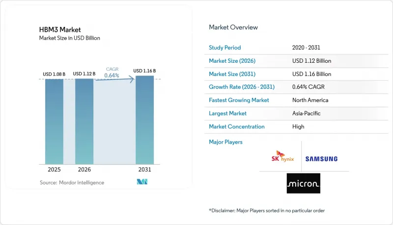
本報告按每堆疊記憶體容量(8 GB 或以下、12-16 GB 及以上)、處理器介面(GPU、CPU、FPGA 及其他)、封裝類型(2.5D、扇出型及其他)、應用領域(AI 訓練、AI 推理、高效能運算伺服器等)、區域供應商等終端服務供應商等終端)和地區供應商等終端)。市場預測以美元計價。
全球 HBM3 市場趨勢與洞察
人工智慧伺服器的擴展和加速運算
儘管最新的設計趨勢轉向了HBM4平台,但從2026年到2031年,對AI伺服器基礎設施的持續投資仍將是HBM3市場最強勁的驅動力。許多企業和二級雲端客戶選擇購買目前已上市、經過認證且更易於整合到現有軟體和散熱環境中的硬體,而不是首批HBM4系統,這一趨勢持續推動了HBM3市場的發展。 SK海力士在2026年展望報告中指出,ASIC相關的HBM需求年增了82%,這表明與加速運算相關的需求正持續擴展到整個買家群體,而不再局限於單一的GPU週期。 H100級叢集也將繼續為HBM3市場提供支持,因為它們的使用壽命跨越了多年的折舊免稅額週期,即使在新平台開始交付後,已部署的系統仍將繼續運作訓練、推理和支持等任務。此外,營運商在將關鍵工作負載遷移到新一代硬體時,還將面臨軟體檢驗和遷移方面的挑戰。因此,HBM3 時代的基礎設施在商業性的重要性將持續比發布計畫所顯示的更長的時間。
先進包裝產能成為新的供應瓶頸。
封裝材料的可用性仍然是HBM3市場面臨的最重要結構性限制之一。這是因為有限的封裝產能減緩了HBM4系統完全取代傳統HBM3設計的速度。因此,HBM3市場受到供應鏈中實際存在的限制因素的支撐。與記憶體晶片的可用性一樣,先進封裝材料的可用性也是決定出貨時間的關鍵因素。每一代產品升級都需要在中介層佈局、穿透矽通孔(TSV)整合、凸塊結構和熱檢驗等方面進行新的工作,這延長了從設計完成到系統全面量產部署的時間。根據2025年電子封裝技術大會上發表的研究,嵌入式橋接晶片中介層是NPU和HBM異構整合的可行方案,推動了企業在封裝形式多樣化方面做出改變,擺脫對傳統中介層過多的依賴。 Synopsys 也討論了其與 Intel Foundry 共同開發的用於更大尺寸的 EMIB-T 封裝,這表明雖然這些替代方案仍需要時間進行規模化和認證,但供應鏈正在積極開發替代方案。
高堆疊裝置中的TSV良率下降和熱節流
隨著堆疊層數的增加,元件良率的下降仍是HBM3市場面臨的直接限制因素。這是因為每增加一個晶片,整個封裝就更有可能無法滿足成本和可靠性目標。因此,儘管市場需求強勁,HBM3市場仍面臨成長瓶頸。堆疊層數的增加雖然提高了密度,但也增加了製造風險和熱集中問題。 MDPI Electronics指出,熱累積仍然是高堆疊HBM結構中長期存在的問題,而混合鍵結技術相比微凸塊互連可以顯著降低熱阻。然而,這種製程改進也帶來了新的學習曲線所帶來的風險。實際上,熱節流會降低高負載下的持續性能,從而削弱在高溫、高密度機架環境中維護老舊HBM3系統的合理性。這些因素將擠壓供應商的利潤空間,降低其相對於新一代記憶體的價格優勢,並減緩HBM3市場的成長速度,即使採購意圖依然樂觀。
細分市場分析
到2025年,12-16GB容量範圍的HBM3銷售量佔比將達到68.12%,成為HBM3市場整體的主導容量等級。這主要歸功於其與H100時代加速系統最大部署基數所使用的參考配置的一致性。這一主導地位反映了HBM3主要引進週期中16GB堆疊的廣泛標準化,並充分考慮了訓練密度、系統平衡以及認證流程的熟練程度。同時,代表早期成本控制型配置的8GB及以下容量級別,由於系統設計人員轉向高密度堆疊以滿足更苛刻的計算工作負載,其銷售貢獻仍然最低。預計到2031年,16GB及以上容量級別將以1.24%的複合年成長率成長,並有望成為HBM3市場中成長最快的容量級別,滿足那些希望獲得更高密度但又不想進行完整平台遷移的買家的需求。 HBM3 產業繼續優先考慮此容量範圍,因為在 HPC 伺服器部署和企業系統整合專案中,堆疊密度和平台連續性仍然比立即遷移到下一代所帶來的增加成本更重要。
該領域的HBM3架構仍受到介面寬度和傳輸容量等標準所定義的技術限制。因此,最高容量等級的產品主要用於頻寬密集型模擬、科學運算和高密度伺服器環境,而非廣泛、低成本的大規模部署。供應商也持續投資於降低高層封裝中翹曲、分層和堆疊應力的技術,因為大規模HBM3堆疊的商業性前景取決於裝置的可靠性,以確保其能夠持續部署。這些努力透過維持高容量選項的商業性可行性,為那些優先考慮部署後生產力而非加速向HBM4過渡的客戶提供支持,從而支撐了HBM3市場。此外,記憶體供應商仍然認為支援HBM3所需的技術投入在經濟上是可行的,這表明該領域在預測期內的大部分時間仍將持續存在。
到了2025年,GPU將佔處理器介面銷售額的73.29%,凸顯HBM3市場對其部署基礎的顯著影響,而該部署基礎正是圍繞NVIDIA H100級訓練基礎架構建構的。這一主導佔有率源自於GPU仍然是大規模AI訓練的基準平台,而大多數HBM3部署都遵循GPU的硬體週期。預計到2031年,AI加速器和ASIC將以1.61%的複合年成長率成長,並有望成為HBM3市場中成長最快的處理器介面細分市場,因為客製化晶片專案擴大了需求基礎。這種轉變使HBM3市場更具韌性,因為主要雲端供應商和平台建構商的客製化加速器專案在同一廣泛的供應生態系統中使用HBM3E,從而降低了買家集中度。因此,HBM3產業將不再那麼依賴單一的商業GPU藍圖,而是與更廣泛、週期更長的運算專案更加緊密地連結在一起。
這一點至關重要,因為客製化加速器的採購通常基於多年配額契約,這提高了內存供應商的可見性,即便商用GPU的世代更迭仍在繼續。 CPU和FPGA介面的貢獻仍然很小,因為在標準部署環境中,電源、控制器複雜性和主流伺服器的經濟性仍然有利於DDR5。然而,基於FPGA的系統在航太、國防和專用嵌入式運算領域繼續發揮重要作用,因為這些專案需要較長的認證週期,並且不會迅速升級到最新一代記憶體。因此,HBM3市場在主要的非GPU領域仍保持著可觀的需求,而這種多元化也是即使在HBM4開始量產後,其銷售額仍保持成長的原因之一。
區域分析
到2025年,亞太地區將佔HBM3市場71.41%的銷售額,成為HBM3市場的核心生產和價值中心。這一地位主要歸功於韓國在TSV堆疊式HBM製造領域的集中佈局,以及台灣在中介層和CoWoS生態系統中的核心地位。 CoWoS生態系統仍是先進封裝(尤其是HBM3系統)組裝的基礎。亞太地區的HBM3市場也受益於先前引進週期中建立的與供應商的牢固關係、工藝知識和製造調整體系,這些優勢在行業經歷代際更迭的過程中依然至關重要。由於2024年底實施的HBM出口管制對先進記憶體准入施加了更嚴格的限制,中國在亞太地區的重要性可能不如其基礎設施需求所顯示的那麼顯著。美國工業與安全局(BIS)已根據出口管制分類編號(ECCN)3A090.c確認了這些HBM限制。這有效地重塑了各地區的市場規模,並迫使一些先進人工智慧記憶體的應用策略調整方向。
預計到2031年,北美地區的複合年成長率將達到1.57%,成為HBM3市場成長最快的區域。該地區的需求成長主要受以下因素驅動:企業IT採購週期落後於超大規模資料中心業者,以及對先進半導體封裝和製造在地化的政策支援。 SK海力士在CHIPS的支持下於印第安納州開展的計畫意義重大,該計畫將成為一個本土封裝和研發中心,恰逢北美企業對HBM3級系統需求強勁的時期。美國國家標準與技術研究院(NIST)已確認將為該項目提供高達4.58億美元的直接資金,預計於2028年下半年開始量產。
歐洲在HBM3市場中保持著雖小但穩定的佔有率。這是因為該地區的採購更多是與機構在高效能運算(HPC)、公共研究系統和系統性技術項目上的支出相關,而非大規模超大規模資料中心業者的硬體升級。因此,該地區的需求較為溫和,採購量有限,但專案在多年採購週期內具有更強的連續性。南美、中東和非洲仍處於HBM3市場的早期需求階段,這些地區的市場活動更可能與邊緣資料中心的擴張、國家主導的人工智慧專案以及進口高速系統相關,而非本地製造。在這些地區,確保供應、認證流程的成熟度和部署速度比即時採用最新一代記憶體更為重要,因此,預計在一段時間內,成熟的基於HBM3的配置仍將繼續被採用。
其他好處:
- Excel格式的市場預測(ME)表
- 3個月的分析師支持
目錄
第1章:引言
- 研究假設和市場定義
- 調查範圍
第2章:調查方法
第3章執行摘要
第4章 市場狀況
- 市場概覽
- 市場促進因素
- 擴展人工智慧伺服器和高速運算的基礎設施。
- 先進包裝產能成為新的供應瓶頸。
- HBM4認證與平台更新周期
- 主權半導體獎勵和區域資本投資
- 利用超大規模資料中心業者進行ASIC的協同設計與記憶體預先分配
- 邊緣人工智慧在汽車和工業系統中的擴展
- 市場限制因素
- 高度堆疊裝置中的TSV良率下降和熱節流
- CoWoS、SoIC 和混合鍵結的產能限制。
- 出口限制和客戶集中風險
- 認證週期長和互通性鎖定
- 產業價值鏈分析
- 供應鏈分析
- 監理情勢
- 技術展望
- 波特五力分析
第5章 市場規模與成長預測
- 每個堆疊的記憶體容量
- 最高可達 8 GB
- 12~16 GB
- 16 GB 或更多
- 透過處理器介面
- GPU
- CPU
- AI加速器和ASIC
- FPGA
- 其他介面
- 按包裝類型
- 2.5D矽膠中介層
- 扇出/嵌入式橋接封裝
- 其他先進封裝
- 透過使用
- 圖形
- 人工智慧訓練
- 人工智慧推理
- 高效能運算 (HPC) 伺服器
- 網路與通訊
- 其他用途
- 產業最終用途
- 雲端服務供應商
- 企業IT
- 電訊
- 車
- 航太/國防
- 其他終端用戶產業
- 按地區
- 北美洲
- 美國
- 加拿大
- 墨西哥
- 歐洲
- 德國
- 英國
- 法國
- 義大利
- 其他歐洲國家
- 亞太地區
- 中國
- 日本
- 韓國
- 台灣
- 印度
- 其他亞太國家
- 南美洲
- 中東和非洲
- 北美洲
第6章 競爭情勢
- 市場集中度
- 策略趨勢
- 市佔率分析
- 公司簡介
- SK hynix Inc.
- Samsung Electronics Co., Ltd.
- Micron Technology, Inc.
- Other Ecosystem Players
- NVIDIA Corporation
- AMD Inc.
- Intel Corporation
- Taiwan Semiconductor Manufacturing Company Limited
- ASE Technology Holding Co., Ltd.
- Amkor Technology, Inc.
- JCET Group Co., Ltd.
- Powertech Technology Inc.
- Rambus Inc.
- Broadcom Inc.
- Marvell Technology, Inc.
- Cadence Design Systems, Inc.
- Synopsys, Inc.
- Applied Materials, Inc.
- Lam Research Corporation
- KLA Corporation
- Tokyo Electron Limited
- Qualcomm Incorporated
第7章 市場機會與未來展望
According to Mordor Intelligence, the HBM3 market size is expected to increase from USD 1.08 billion in 2025 to USD 1.12 billion in 2026 and reach USD 1.16 billion by 2031, growing at a CAGR of 0.64% over 2026-2031.
This report is Segmented by Memory Capacity Per Stack (Up To 8 GB, 12 To 16 GB, and More), Processor Interface (GPU, CPU, FPGA, and More), Packaging Type (2. 5D, Fan-Out, and More), Application (AI Training, AI Inference, High-Performance Computing Servers, and More), End Use Industry (Cloud Service Providers, and More), and Geography (North America, and More). The Market Forecasts are Provided in Terms of Value (USD).
Global HBM3 Market Trends and Insights
AI Server and Accelerated Computing Buildout
Sustained spending on AI server infrastructure remains the strongest support factor for the HBM3 market during 2026-2031, even as the latest design wins are shifting toward HBM4 platforms. The HBM3 market still benefits from the fact that many enterprise and second-tier cloud customers are buying hardware that is available now, qualified now, and easier to integrate into existing software and cooling environments than first-wave HBM4 systems. SK hynix stated in its 2026 outlook that ASIC-related HBM demand grew 82% year over year, indicating that demand tied to accelerated computing is still widening across buyer groups rather than narrowing around a single GPU cycle. H100-class clusters also continue to support the HBM3 market because their useful life spans multi-year depreciation schedules, keeping deployed systems active in training, inference, and support roles after newer platforms begin shipping. Operators also face software validation and migration work when they move critical workloads to a new hardware generation, and that makes HBM3-era infrastructure commercially relevant for longer than a simple launch timeline would suggest.
Advanced Packaging Capacity as the New Supply Bottleneck
Packaging availability remains one of the clearest structural supports for the HBM3 market because limited packaging throughput slows the rate at which HBM4 systems can fully replace earlier HBM3-based designs. The HBM3 market is therefore helped by a practical constraint in the supply chain, since advanced packaging slots determine shipment timing just as much as memory die availability does. Each generational transition requires renewed work on interposer layouts, through-silicon via integration, bump structures, and thermal validation, which lengthens the path from engineering readiness to volume system deployment. Research presented at the 2025 Electronics Packaging Technology Conference showed that embedded bridge die interposers are a viable route for heterogeneous integration of NPUs and HBM, supporting the broader industry push to diversify packaging formats beyond conventional interposer-heavy approaches. Synopsys also described its work with Intel Foundry on EMIB-T packaging for larger form factors, demonstrating that the supply chain is actively developing alternatives, even though those alternatives still need time to scale and qualify.
TSV Yield Losses and Thermal Throttling in High-Stack Devices
Yield loss in taller stacked devices remains a direct constraint on the HBM3 market, as each additional die increases the likelihood that the full package will fail to meet cost or reliability targets. The HBM3 market, therefore, faces a ceiling even when demand is healthy, since higher stack counts improve density but also raise manufacturing risk and heat concentration. MDPI Electronics noted that thermal accumulation remains a persistent issue in high-layer HBM structures and that hybrid bonding can materially reduce thermal resistance compared with microbump interconnects, even though the process shift introduces a fresh learning-curve risk of its own. In practice, thermal throttling reduces sustained performance under demanding workloads, weakening the economic case for keeping older HBM3 systems in the hottest, most densely utilized rack environments. These factors compress supplier margins, narrow the price advantage over newer memory generations, and slow the rate of HBM3 market growth, even when procurement intent remains positive.
Other drivers and restraints analyzed in the detailed report include:
- HBM4 Qualification and Platform Refresh Cycles
- Sovereign Semiconductor Incentives and Localized Capex
- CoWoS, SoIC, and Hybrid Bonding Capacity Constraints
For complete list of drivers and restraints, kindly check the Table Of Contents.
Segment Analysis
The 12-16 GB tier accounted for 68.12% of HBM3 revenue in 2025, making it the dominant capacity class across the HBM3 market, as it matched the reference configuration used in the largest installed base of H100-era accelerated systems. That leading position reflected broad standardization around 16 GB stacks for training density, system balance, and qualification familiarity during the main HBM3 deployment cycle. The up to 8 GB segment, which represented earlier, more cost-sensitive configurations, remained the smallest revenue contributor as system designers shifted toward denser stacks for advanced compute workloads. The above 16 GB tier is projected to grow at a 1.24% CAGR through 2031, making it the fastest-growing capacity range in the HBM3 market for buyers who want higher density without forcing a full platform migration. The HBM3 industry keeps this tier relevant because HPC server deployments and enterprise consolidation programs still value stack density and platform continuity over the higher cost of jumping immediately to the next generation.
HBM3 architecture in this segment remains tied to standards-defined technical limits on interface width and transfer capability, which is why the most advanced capacity points are used in bandwidth-intensive simulation, scientific computing, and tightly packed server environments rather than in broad, low-cost volume deployment. Suppliers also continue to invest in methods that reduce warpage, delamination, and stack stress in high-layer packages, since the commercial future of larger HBM3 stacks depends on making those devices reliable enough for sustained deployment. That effort supports the HBM3 market by keeping higher-capacity options commercially viable for customers who care more about deployed productivity than about being first to move to HBM4. It also suggests that the segment will remain available throughout most of the forecast period because the technical work required to support it is still considered economically meaningful by memory vendors.
GPU held 73.29% of processor interface revenue in 2025, underscoring how strongly the HBM3 market was shaped by the installed base built around NVIDIA H100-class training infrastructure. That dominance came from the fact that GPU remained the reference platform for large-scale AI training, and the bulk of HBM3 deployment followed that hardware cycle. AI accelerators and ASICs are projected to grow at a 1.61% CAGR through 2031, making it the fastest-growing processor interface segment in the HBM3 market as custom silicon programs expand the demand base. The HBM3 market gains resilience from this shift because buyer concentration falls when custom accelerator projects from large cloud operators and platform builders consume HBM3E within the same broader supply ecosystem. The HBM3 industry, therefore, becomes less dependent on one merchant GPU roadmap and more tied to a broader set of long-cycle compute programs.
This matters because custom accelerator procurement often runs on multi-year allocation agreements, which improve visibility for memory suppliers even as public GPU cycles transition to newer generations. CPU and FPGA interfaces remain smaller contributors because power delivery, controller complexity, and mainstream server economics still favor DDR5 in standard deployments. Even so, FPGA-based systems continue to matter in aerospace, defense, and specialized embedded compute because these programs undergo long qualification windows and do not migrate quickly to the latest memory generation. The HBM3 market, therefore, retains useful demand outside the main GPU base, and that diversification helps explain why revenue remains positive even after HBM4 entered production.
Complete Report Scope:
- By Memory Capacity Per Stack
- Up to 8 GB
- 12 to 16 GB
- Above 16 GB
- By Processor Interface
- GPU
- CPU
- AI Accelerator and ASIC
- FPGA
- Other Interfaces
- By Packaging Type
- 2.5D Silicon Interposer
- Fan-Out / Embedded Bridge Packaging
- Other Advanced Packaging
- By Application
- Graphics
- AI Training
- AI Inference
- High-Performance Computing (HPC) Servers
- Networking and Telecommunications
- Other Applications
- By End Use Industry
- Cloud Service Providers
- Enterprise IT
- Telecommunications
- Automotive
- Aerospace and Defense
- Other End-user Industries
- By Geography
- North America
- United States
- Canada
- Mexico
- Europe
- Germany
- United Kingdom
- France
- Italy
- Rest of Europe
- Asia-Pacific
- China
- Japan
- South Korea
- Taiwan
- India
- Rest of Asia-Pacific
- South America
- Middle East and Africa
- North America
Geography Analysis
Asia-Pacific accounted for 71.41% of revenue in 2025, making it the core production and value center of the HBM3 market. That position comes from South Korea's concentration in TSV-stacked HBM manufacturing and Taiwan's central role in advanced packaging, especially in the interposer and CoWoS ecosystem that still underpins much of HBM3 system assembly. The HBM3 market in Asia-Pacific also benefits from deep supplier relationships, process knowledge, and manufacturing coordination built during earlier deployment cycles that remain useful as the industry navigates a generational transition. China's role in the broader region is more limited than pure infrastructure demand might suggest, because HBM export restrictions introduced a harder boundary on advanced memory access from late 2024. The Bureau of Industry and Security confirmed those controls on HBM under ECCN 3A090.c, effectively reshaping the regional addressable base and redirecting part of the deployment logic for advanced AI memory.
North America is projected to grow at a 1.57% CAGR through 2031, making it the fastest-growing regional block in the HBM3 market. Demand in this region is supported by enterprise IT procurement cycles that trail hyperscaler adoption and by the growing policy push to localize advanced semiconductor packaging and manufacturing. The SK hynix CHIPS-backed Indiana project is important here because it creates a domestic packaging and research-and-development anchor that aligns with the period when North American enterprise demand for HBM3-class systems remains active. The National Institute of Standards and Technology confirmed that the project includes up to USD 458 million in direct funding and is expected to enter mass production in the second half of 2028.
Europe remains a smaller but steady part of the HBM3 market because procurement is tied more closely to institutional HPC spending, public research systems, and structured technology programs than to large-scale hyperscaler hardware refreshes. That gives the region a more measured demand profile, with volume limited but program continuity stronger across multi-year procurement cycles. South America, the Middle East, and Africa remain early-stage demand pools in the HBM3 market, and their activity is likely to be linked to edge data center buildout, sovereign AI programs, and imported, accelerated systems rather than local fabrication. These regions are likely to keep using proven HBM3-based configurations in the near term because supply accessibility, qualification maturity, and deployment speed remain more important than immediate adoption of the newest memory generation.
- SK hynix Inc.
- Samsung Electronics Co., Ltd.
- Micron Technology, Inc.
Additional Benefits:
- The market estimate (ME) sheet in Excel format
- 3 months of analyst support
TABLE OF CONTENTS
1 INTRODUCTION
- 1.1 Study Assumptions and Market Definition
- 1.2 Scope of the Study
2 RESEARCH METHODOLOGY
3 EXECUTIVE SUMMARY
4 MARKET LANDSCAPE
- 4.1 Market Overview
- 4.2 Market Drivers
- 4.2.1 AI Server and Accelerated Computing Buildout
- 4.2.2 Advanced Packaging Capacity as the New Supply Bottleneck
- 4.2.3 HBM4 Qualification and Platform Refresh Cycles
- 4.2.4 Sovereign Semiconductor Incentives and Localized Capex
- 4.2.5 Hyperscaler ASIC Co-Design and Memory Pre-Allocation
- 4.2.6 Edge AI Expansion in Automotive and Industrial Systems
- 4.3 Market Restraints
- 4.3.1 TSV Yield Losses and Thermal Throttling in High-Stack Devices
- 4.3.2 CoWoS, SoIC, and Hybrid Bonding Capacity Constraints
- 4.3.3 Export Controls and Customer Concentration Risk
- 4.3.4 Long Qualification Cycles and Interoperability Lock-In
- 4.4 Industry Value Chain Analysis
- 4.5 Supply Chain Analysis
- 4.6 Regulatory Landscape
- 4.7 Technological Outlook
- 4.8 Porter's Five Forces Analysis
- 4.8.1 Threat of New Entrants
- 4.8.2 Bargaining Power of Suppliers
- 4.8.3 Bargaining Power of Buyers
- 4.8.4 Threat of Substitutes
- 4.8.5 Intensity of Competitive Rivalry
5 MARKET SIZE AND GROWTH FORECASTS (VALUE)
- 5.1 By Memory Capacity Per Stack
- 5.1.1 Up to 8 GB
- 5.1.2 12 to 16 GB
- 5.1.3 Above 16 GB
- 5.2 By Processor Interface
- 5.2.1 GPU
- 5.2.2 CPU
- 5.2.3 AI Accelerator and ASIC
- 5.2.4 FPGA
- 5.2.5 Other Interfaces
- 5.3 By Packaging Type
- 5.3.1 2.5D Silicon Interposer
- 5.3.2 Fan-Out / Embedded Bridge Packaging
- 5.3.3 Other Advanced Packaging
- 5.4 By Application
- 5.4.1 Graphics
- 5.4.2 AI Training
- 5.4.3 AI Inference
- 5.4.4 High-Performance Computing (HPC) Servers
- 5.4.5 Networking and Telecommunications
- 5.4.6 Other Applications
- 5.5 By End Use Industry
- 5.5.1 Cloud Service Providers
- 5.5.2 Enterprise IT
- 5.5.3 Telecommunications
- 5.5.4 Automotive
- 5.5.5 Aerospace and Defense
- 5.5.6 Other End-user Industries
- 5.6 By Geography
- 5.6.1 North America
- 5.6.1.1 United States
- 5.6.1.2 Canada
- 5.6.1.3 Mexico
- 5.6.2 Europe
- 5.6.2.1 Germany
- 5.6.2.2 United Kingdom
- 5.6.2.3 France
- 5.6.2.4 Italy
- 5.6.2.5 Rest of Europe
- 5.6.3 Asia-Pacific
- 5.6.3.1 China
- 5.6.3.2 Japan
- 5.6.3.3 South Korea
- 5.6.3.4 Taiwan
- 5.6.3.5 India
- 5.6.3.6 Rest of Asia-Pacific
- 5.6.4 South America
- 5.6.5 Middle East and Africa
- 5.6.1 North America
6 COMPETITIVE LANDSCAPE
- 6.1 Market Concentration
- 6.2 Strategic Moves
- 6.3 Market Share Analysis
- 6.4 Company Profiles (includes Global Level Overview, Market Level Overview, Core Segments, Financials as available, Strategic Information, Products and Services, Recent Developments)
- 6.4.1 SK hynix Inc.
- 6.4.2 Samsung Electronics Co., Ltd.
- 6.4.3 Micron Technology, Inc.
- 6.5 Other Ecosystem Players
- 6.5.1 NVIDIA Corporation
- 6.5.2 AMD Inc.
- 6.5.3 Intel Corporation
- 6.5.4 Taiwan Semiconductor Manufacturing Company Limited
- 6.5.5 ASE Technology Holding Co., Ltd.
- 6.5.6 Amkor Technology, Inc.
- 6.5.7 JCET Group Co., Ltd.
- 6.5.8 Powertech Technology Inc.
- 6.5.9 Rambus Inc.
- 6.5.10 Broadcom Inc.
- 6.5.11 Marvell Technology, Inc.
- 6.5.12 Cadence Design Systems, Inc.
- 6.5.13 Synopsys, Inc.
- 6.5.14 Applied Materials, Inc.
- 6.5.15 Lam Research Corporation
- 6.5.16 KLA Corporation
- 6.5.17 Tokyo Electron Limited
- 6.5.18 Qualcomm Incorporated
7 MARKET OPPORTUNITIES AND FUTURE OUTLOOK
- 7.1 White-Space and Unmet-Need Assessment

 ESG資料智慧平台市場預測至2034年-按智慧類型、資料來源、分析技術、部署模式、最終使用者和地區分類的全球分析語意層市場預測至 2034 年—按元件、部署模式、架構、資料來源、應用、最終使用者和區域分類的全球分析
 AI加速器DRAM市佔率分析、產業趨勢與統計及成長預測(2026-2031年)GDDR7 市佔率分析(適用於 AI 推理 GPU)、產業趨勢與統計及成長預測(2026-2031 年)
 克服記憶體瓶頸:CXL擴展和KV快取壓縮創新HBM3E:市場佔有率分析、產業趨勢與統計、成長預測(2026-2031)以人工智慧工作負載的 CXL 記憶體擴展:市場佔有率分析、行業趨勢與統計數據以及成長預測(2026-2031 年)衛星資料分析市場預測至2034年-按分析方法、資料類型、部署方式、應用、最終用戶和地區分類的全球分析
 2026年全球合成電子健康紀錄(EHR)資料產生平台市場報告人工智慧開發工具市場預測——全球分析(按組件、工具類型、部署模式、組織規模、技術、應用、最終用戶和地區分類)——2034年