


 |
市場調查報告書
商品編碼
2099847
AI加速器DRAM市佔率分析、產業趨勢與統計及成長預測(2026-2031年)DRAM For AI Accelerator - Market Share Analysis, Industry Trends & Statistics, Growth Forecasts (2026 - 2031) |
||||||

※ 本網頁內容可能與最新版本有所差異。詳細情況請與我們聯繫。
據 Mordor Intelligence 稱,2025 年 AI 加速器中 DRAM 的市場規模為 188 億美元,預計從 2026 年到 2031 年將以 27.3% 的複合年成長率成長,到 2031 年達到 829 億美元。
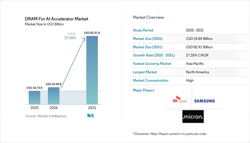
本報告依記憶體架構(基於HBM的DRAM、基於GDDR的DRAM、基於DDR的DRAM)、AI加速器類型(GPU、AI加速器ASIC、FPGA、具備AI加速功能的CPU)、單模組/單堆疊容量(最高16GB、16GB至32GB、32GB至64GB、64GB市場預測以美元(USD)計價。
全球DRAM市場趨勢及AI加速器洞察
HBM在AI GPU平台的搭載率不斷提高
隨著領先的AI GPU將HBM記憶體不再僅僅視為可選記憶體選項,而是將其視為核心要求,AI加速器領域的DRAM市場正在不斷擴張。 NVIDIA的B200晶片配備了192GB的HBM3e頻寬8TB/s;而Rubin系列GPU的HBM4內存容量可擴展至每顆GPU 288GB。 NVIDIA表示,在機架級規模下,72顆Rubin GPU將整合HBM內存,形成一個13.5TB的連貫內存架構,這充分展現了內存容量和互連設計的演進。即使加速器出貨量的成長不再呈線性,隨著每台部署設備的記憶體容量不斷增加,這種架構仍將維持對HBM記憶體的高需求。谷歌在2026年6月發布的關於TPU系統演進的論文也證實,在五代技術發展過程中,每個訓練節點的HBM記憶體容量和頻寬將會成長十倍。在AI加速器的DRAM市場,隨著每個運算節點的記憶體容量在每個平台週期中持續成長,這一趨勢將支撐其價值的持續成長。
從通用DRAM過渡到頻寬最佳化型記憶體堆疊
AI加速器領域的DRAM市場正在不斷發展,部分原因是記憶體討論的重點已從簡單的容量轉向頻寬效率和堆疊架構。 2025年4月,JEDEC發布了JESD270-4 HBM4標準,定義了2048位元介面、32個獨立通道、最大資料速率8Gbps以及每個堆疊最高支援64GB的容量。該標準的發布意義重大,因為它為採購商和系統設計人員提供了下一代記憶體互通性的明確標準。 2025年12月,JEDEC繼續推進標準化進程,宣布了其在SPHBM4方面的努力,SPHBM4在減少引腳數量的同時實現了與HBM4相當的吞吐量。因此,AI加速器領域的DRAM市場正受益於頻寬頻寬最佳化堆疊的系統性轉變,而不是迭代地調整傳統的DRAM格式。這項變更也延長了HBM平台的產品週期,因為客戶現在可以基於標準的擴展性進行規劃,而不是採用一次性的實現方案。
HBM封裝瓶頸和先進基板產能限制
儘管記憶體需求持續強勁,但面向人工智慧加速器的DRAM市場在先進封裝技術和基板準備方面仍面臨許多限制。三星的商用HBM4專案採用4nm製程晶片,單堆疊容量高達3.3 TB/s,展現了目前尖端人工智慧記憶體產品所需的製程整合水準。 2026年7月,三星電子和SK海力士宣布投資240兆韓元(約1,550億美元)在忠清地區建造新的HBM製造廠和先進封裝設施。這清楚地顯示下游產能仍需大幅提升。如此大規模的投資表明,封裝仍然是一個重要的瓶頸,影響供應商的策略和區域資本配置。如果封裝生產線產能無法跟上晶圓生產,僅靠記憶體晶片不足以供應成品加速器。因此,儘管產能投資不斷加速,面向人工智慧加速器的DRAM市場仍面臨短期供應短缺的問題。
細分市場分析
預計到2025年,基於HBM的DRAM將佔據AI加速器DRAM市場78.4%的佔有率,並將在2031年之前以28.2%的複合年成長率成長。這項領先優勢反映出,AI加速器的記憶體選擇如今不再僅基於傳統的每位元成本邏輯,而是基於頻寬、密度和系統效率。谷歌於2026年6月發表的一篇關於TPU的論文顯示,HBM的容量和每個訓練節點的頻寬在五代產品中成長了十倍,這解釋了為什麼HBM已從高階選項轉變為核心平台要求。 JEDEC HBM4標準正式定義了這一轉變的下一步,其單棧容量高達64 GB,並顯著擴展了介面結構以支援高吞吐量計算。在AI加速器的DRAM產業中,這些優勢使得HBM成為尖端AI部署的標竿架構。
基於 GDDR 的 DRAM 在 AI 加速器的 DRAM 市場中仍佔據重要地位。在這個市場中,對成本敏感的推理系統需要比大量使用 HBM 的訓練硬體更低的記憶體成本。它的作用在需要足夠頻寬且能夠容忍一定封裝複雜性的工作負載中最為明顯。基於 DDR 的 DRAM 仍然應用於 AI 伺服器的系統記憶體層,支援編配、資料傳輸和主機端緩衝,而不是直接用於高頻寬加速器的執行。雖然隨著機架級 AI 系統整合度的提高,DDR 仍然很重要,但其戰略角色正在從核心加速器記憶體轉向支援整個伺服器設計的記憶體。因此,AI 加速器中的 DRAM 市場尚未完全與其他記憶體類型分離,但它們在以 HBM 為中心的架構堆疊中所扮演的角色正在明顯縮小。
在2025年的AI加速器DRAM市場中,GPU平台佔據了74.4%的佔有率,而AI加速器ASIC預計到2031年將以28.2%的年均成長率成長。 GPU之所以繼續保持主導地位,是因為它們仍然是超大規模資料中心業者訓練叢集的預設選擇,並且與各種AI軟體相容。同時,隨著主要雲端服務供應商要求更嚴格的成本控制以及記憶體、互連和模型服務操作之間更緊密的協調,客製化ASIC專案正在蓬勃發展。谷歌的TPU 8i擁有288 GB的HBM和8601 GB/s的頻寬,這表明客製化開發的加速器正在迅速縮小與主流GPU平台的效能差距。在AI加速器DRAM市場,這意味著採購成長正在超越單一的主導加速器類別,儘管GPU仍然擁有最大的部署基礎。
基於FPGA的加速器雖然市佔率較小,但在低延遲通訊、金融運算和可重構性至關重要的特定部署情境中,它們仍然具有價值。具備AI加速功能的CPU在企業推理環境中也保持著一定的地位,因為在這些環境中,與現有伺服器基礎設施的兼容性和廣泛的軟體支援是優先考慮的因素。因此,AI加速器中的DRAM市場並非單一的硬體模板,而是與多種運算路徑相關聯。儘管如此,成長的主要動力仍然轉向能夠支援大規模容量HBM和高並行記憶體吞吐量的產品。因此,雖然GPU仍然是目前DRAM出貨量的主要驅動力,但ASIC正在塑造AI加速器DRAM市場中未來記憶體需求成長最快的領域。
區域分析
2025年,北美佔據了人工智慧加速器DRAM市場44.9%的佔有率。這一主導地位源自於美國大型超大規模資料中心業者持續集中於此的資本投資項目,以及對模型開發和人工智慧基礎設施建設的持續關注。這種需求模式意味著,即使生產地點不在北美,人工智慧加速器DRAM市場也與微軟、Google、亞馬遜和Meta等公司的採購趨勢緊密相關。此外,美國也主導了先進記憶體的法規環境。美國工業與安全局(BIS)於2024年12月將HBM列入出口管制分類編號(ECCN)3A090.c,並將相關出口限制擴展至中國大陸和澳門。這進一步鞏固了北美在其盟友供應鏈中的核心地位。
歐洲在人工智慧加速器的DRAM市場中仍是一個相對小規模的區域板塊,但其需求正從低位穩定成長。該地區受益於各國政府主導的人工智慧計畫、對本地資料中心的投資以及企業對滿足資料居住要求的推理基礎設施的濃厚興趣。這促使歐洲的部署趨勢更加穩定,優先考慮的是可管理的部署和合規性,而不是規模最大的前緣訓練叢集。儘管該地區目前的支出規模落後於北美,但由於本地部署需求持續推動對高頻寬人工智慧系統的需求,它仍然是一個重要的市場。
亞太地區是人工智慧加速器DRAM市場成長最快的區域市場,預計到2031年複合年成長率將達到28.1%。該地區既是先進DRAM的主要生產中心,也是人工智慧運算基礎設施需求不斷成長的中心,扮演著雙重角色。 2026年7月,三星電子和SK海力士決定投資240兆韓元(約1550億美元),在韓國忠清道建造一座新的HBM製造工廠和先進封裝設施。同樣在2026年7月,美光科技在廣島啟動了一個擴建項目,以增強其在日本的HBM產能。雖然「其他全球市場」仍處於起步階段,但中東部分地區政府主導的人工智慧投資正開始將人工智慧加速器DRAM的需求擴展到新的地區。
其他好處:
- Excel格式的市場預測(ME)表
- 3個月的分析師支持
目錄
第1章:引言
- 研究假設和市場定義
- 調查範圍
第2章:調查方法
第3章執行摘要
第4章 市場狀況
- 市場概覽
- 市場促進因素
- HBM在AI GPU平台的搭載率不斷提高
- 從通用DRAM過渡到頻寬最佳化型記憶體堆疊
- 人工智慧伺服器叢集對記憶體密度的需求正在迅速成長。
- 多GPU伺服器配置的增加以及對記憶體池需求的成長。
- 提高高分子骨材供應鏈的產量並擴大產能
- 在注重成本效益的人工智慧推理GPU中擴大GDDR的使用
- 市場限制因素
- HBM封裝瓶頸和先進基板生產能力的限制。
- 新DRAM供應商的進入門檻很高
- 由於通用伺服器對DDR記憶體的需求,記憶體分配競爭加劇。
- 出口限制和地緣政治限制對先進記憶體的供應造成限制
- 產業供應鏈分析
- 監理情勢
- 技術展望
- 宏觀經濟因素對市場的影響
- 波特五力分析
第5章 市場規模與成長預測
- 依記憶體架構
- 基於HBM的DRAM
- 基於GDDR的DRAM
- 基於DDR的DRAM
- AI加速器類型
- GPU
- AI加速器ASIC
- FPGA
- 具備AI加速功能的CPU
- 每個模組或堆疊的容量
- 最高可達 16GB
- 16 GB~32 GB
- 32 GB~64 GB
- 64 GB~128 GB
- 128 GB 或更多
- 透過使用
- 訓練
- 推理
- 高效能運算
- 商用視覺化
- 最終用戶
- 超大規模雲端服務供應商
- AI伺服器和系統OEM製造商
- 半導體公司
- 研究和學術機構
- 按地區
- 北美洲
- 歐洲
- 亞太地區
- 中國
- 日本
- 韓國
- 台灣
- 其他亞太國家
- 世界其他地區
第6章 競爭情勢
- 市場集中度
- 策略趨勢
- 市佔率分析
- 公司簡介
- SK Hynix Inc.
- Samsung Electronics Co., Ltd.
- Micron Technology, Inc.
- NVIDIA Corporation
- Advanced Micro Devices, Inc.
- Intel Corporation
- SK Hynix System IC Inc.
- Rambus Inc.
- United Microelectronics Corporation
- Taiwan Semiconductor Manufacturing Company Limited
- Amkor Technology, Inc.
- ASE Technology Holding Co., Ltd.
- Micron Semiconductor Asia Pte. Ltd.
- Samsung Semiconductor, Inc.
- Kingston Technology Company, Inc.
- G.SKILL International Enterprise Co., Ltd.
- Corsair Gaming, Inc.
- Team Group Inc.
- Powerchip Semiconductor Manufacturing Corporation
- Nanya Technology Corporation
第7章 市場機會與未來展望
According to Mordor Intelligence, the DRAM for AI accelerator market size was valued at USD 18.8 billion in 2025 and is forecast to reach USD 82.9 billion by 2031, at a CAGR of 27.3% from 2026 to 2031.
This report is Segmented by Memory Architecture (HBM-Based DRAM, GDDR-Based DRAM, and DDR Based DRAM), AI Accelerator Type (GPU, AI Accelerator ASIC, FPGA, and CPU With AI Acceleration), Capacity Per Module/Stack (Up To 16 GB, 16 GB To 32 GB, 32 GB To 64 GB, 64 GB To 128 GB, and More), Application (Training, Inference, and More), and Geography. The Market Forecasts are Provided in Terms of Value (USD).
Global DRAM For AI Accelerator Market Trends and Insights
Rising HBM Attach Rates in AI GPU Platforms
The DRAM for AI accelerator market is being pushed higher as leading AI GPUs now treat HBM as a core requirement rather than an optional memory choice. NVIDIA's B200 carries 192 GB of HBM3e at 8 TB/s bandwidth, and the Rubin generation scales to 288 GB of HBM4 per GPU. At rack scale, NVIDIA stated that 72 Rubin GPUs pool their HBM into a 13.5 TB coherent memory fabric, demonstrating how memory capacity and interconnect design are advancing together. That architecture keeps HBM demand high even if accelerator shipment growth becomes less linear, because more memory is being attached to each deployed device. Google's June 2026 paper on TPU system evolution also confirmed a 10x increase in HBM capacity and bandwidth per training node across five generations. In the DRAM for AI accelerator market, that pattern supports sustained value growth because memory content per compute node continues to increase with each platform cycle.
Shift From General-Purpose DRAM to Bandwidth-Optimized Memory Stacks
The DRAM for AI accelerator market is also advancing because the memory discussion has shifted from raw capacity toward bandwidth efficiency and stack architecture. JEDEC released the JESD270-4 HBM4 standard in April 2025, defining a 2,048-bit interface, 32 independent channels, data rates up to 8 Gbps, and support for up to 64 GB per stack. That publication matters because it gives buyers and system designers a clear interoperability baseline for the next memory generation. The same standards path continued in December 2025, when JEDEC disclosed work on SPHBM4 to deliver HBM4-level throughput with reduced pin count. As a result, DRAM for AI accelerator market is benefiting from a more formal migration toward bandwidth-optimized stacks rather than repeated tuning of conventional DRAM formats. This change also supports longer product cycles for HBM platforms because customers can now plan around standards-based scaling rather than one-off implementation paths.
HBM Packaging Bottlenecks and Limited Advanced Substrate Capacity
The DRAM for AI accelerator market continues to face a real cap from advanced packaging and substrate readiness, even as memory demand remains strong. Samsung's commercial HBM4 program uses a 4nm base die and achieves up to 3.3 TB/s per stack, demonstrating the level of process integration now required for leading AI memory products. In July 2026, Samsung Electronics and SK Hynix committed KRW 240 trillion (USD 155 billion) in the Chungcheong region to new HBM fabrication plants and advanced packaging facilities, underscoring the extent of downstream capacity that still needs to be built. The scale of that investment shows that packaging remains a bottleneck large enough to shape supplier strategy and regional capital allocation. When packaging lines lag wafer output, memory dies alone do not translate into a finished accelerator supply. That is why the DRAM for AI accelerator market still faces near-term supply friction, even while spending on capacity is accelerating.
Other drivers and restraints analyzed in the detailed report include:
- Rapid Growth in AI Server Cluster Memory Density Requirements
- Increase in Multi-GPU Server Configurations and Memory Pooling Demand
- High Qualification Barriers for New DRAM Suppliers
For complete list of drivers and restraints, kindly check the Table Of Contents.
Segment Analysis
HBM-Based DRAM held 78.4% of the DRAM for AI accelerator market share in 2025, and is also projected to expand at a 28.2% CAGR through 2031. That lead reflects how AI accelerator memory is now being selected on bandwidth, density, and system efficiency rather than on conventional cost-per-bit logic alone. Google's June 2026 TPU paper showed a 10x increase in HBM capacity and bandwidth per training node across five generations, which helps explain why HBM has moved from a premium option to a core platform requirement. JEDEC's HBM4 standard also formalized the next step in this migration, with up to 64 GB per stack and a much wider interface structure for high-throughput computing. In the DRAM for AI accelerator industry, that combination makes HBM the reference architecture for frontier AI deployments.
GDDR-Based DRAM remains relevant in the DRAM for AI accelerator market, where cost-sensitive inference systems need a lower memory bill than HBM-heavy training hardware. Its role is strongest in workloads that can accept lower packaging complexity while still requiring meaningful bandwidth. DDR-Based DRAM continues to sit in the system memory layer of AI servers, where it supports orchestration, data movement, and host-side buffering rather than direct high-bandwidth accelerator execution. As rack-scale AI systems become more coherent, DDR still matters, but its strategic role is shifting from core accelerator memory toward support memory across the full server design. The result is that the DRAM for AI accelerator market is not moving entirely away from other memory types, but it is clearly assigning them narrower roles within an HBM-centered architecture stack.
GPU platforms accounted for 74.4% of the DRAM for AI accelerator market size in 2025, while AI accelerator ASICs are forecast to grow at 28.2% through 2031. GPUs keep the lead because they remain the default choice for hyperscaler training clusters and broad AI software compatibility. At the same time, custom ASIC programs are gaining traction because large cloud providers want better cost control and tighter alignment between memory, interconnect, and model-serving behavior. Google's TPU 8i features 288 GB of HBM and 8,601 GB/s of bandwidth, demonstrating how quickly proprietary accelerator programs are closing the capability gap with mainstream GPU platforms. In the DRAM for AI accelerator market, this means procurement growth is expanding beyond a single dominant accelerator category, even as GPUs still control the largest installed base.
FPGA-based accelerators hold a smaller position, but they retain value in low-latency communications, financial computing, and targeted deployment environments where reconfigurability remains important. CPUs with AI acceleration also maintain a place in enterprise inference setups that prioritize compatibility with established server infrastructure and broader software support. That keeps the DRAM for AI accelerator market tied to multiple compute paths rather than a single hardware template. Even so, the strongest growth pressure is still shifting toward products that can support large HBM footprints and high parallel memory throughput. The net effect is that GPUs continue to define present-day volume, while ASICs are shaping where future memory demand expands fastest in the DRAM for AI accelerator market.
Complete Report Scope:
- By Memory Architecture
- HBM Based DRAM
- GDDR Based DRAM
- DDR Based DRAM
- By AI Accelerator Type
- GPU
- AI Accelerator ASIC
- FPGA
- CPU with AI Acceleration
- By Capacity Per Module or Stack
- Up to 16 GB
- 16 GB to 32 GB
- 32 GB to 64 GB
- 64 GB to 128 GB
- Above 128 GB
- By Application
- Training
- Inference
- High Performance Computing
- Professional Visualization
- By End User
- Hyperscale Cloud Service Providers
- AI Server and System OEMs
- Semiconductor Companies
- Research and Academic Institutions
- By Geography
- North America
- Europe
- Asia Pacific
- China
- Japan
- South Korea
- Taiwan
- Rest of Asia Pacific
- Rest of the World
Geography Analysis
North America represented 44.9% of the DRAM for AI accelerator market size in 2025. The region leads because the largest hyperscaler capital programs remain concentrated in the United States, where model development and AI infrastructure build-outs are still centered. That demand pattern keeps the DRAM for AI accelerator market closely tied to the purchasing behavior of Microsoft, Google, Amazon, and Meta, even when production takes place elsewhere. The United States also shapes the regulatory environment for advanced memory. The Bureau of Industry and Security added HBM to ECCN 3A090.c in its December 2024 rule and extended related export controls to shipments involving China and Macau, thereby reinforcing North America's central role in the allied-country supply chain.
Europe remains a smaller regional block in the DRAM for AI accelerator market, and its demand is rising from a lower starting base. The region is supported by sovereign AI programs, local data center investments, and enterprise interest in inference infrastructure that meets data residency requirements. That gives Europe a steadier adoption profile, with greater emphasis on controlled deployment and compliance-readiness than on the largest frontier training clusters. The region does not yet match North America on spending scale, but it remains relevant because local deployment requirements continue to create demand for high-bandwidth AI systems.
Asia-Pacific is the fastest-growing regional segment in the DRAM for AI accelerator market, with a projected CAGR of 28.1% through 2031. The region plays a dual role as both the main production base for advanced DRAM and a rising demand center for AI compute infrastructure. In July 2026, Samsung Electronics and SK Hynix committed KRW 240 trillion, or USD 155 billion, in South Korea's Chungcheong region for new HBM fabrication plants and advanced packaging facilities. Micron also broke ground on its Hiroshima expansion in July 2026 to strengthen HBM production capacity in Japan. The Rest of the World segment remains early-stage, but sovereign AI spending in parts of the Middle East is beginning to pull more of the DRAM for AI accelerator market into new deployment geographies.
- SK Hynix Inc.
- Samsung Electronics Co., Ltd.
- Micron Technology, Inc.
- NVIDIA Corporation
- Advanced Micro Devices, Inc.
- Intel Corporation
- SK Hynix System IC Inc.
- Rambus Inc.
- United Microelectronics Corporation
- Taiwan Semiconductor Manufacturing Company Limited
- Amkor Technology, Inc.
- ASE Technology Holding Co., Ltd.
- Micron Semiconductor Asia Pte. Ltd.
- Samsung Semiconductor, Inc.
- Kingston Technology Company, Inc.
- G.SKILL International Enterprise Co., Ltd.
- Corsair Gaming, Inc.
- Team Group Inc.
- Powerchip Semiconductor Manufacturing Corporation
- Nanya Technology Corporation
Additional Benefits:
- The market estimate (ME) sheet in Excel format
- 3 months of analyst support
TABLE OF CONTENTS
1 INTRODUCTION
- 1.1 Study Assumptions and Market Definition
- 1.2 Scope of the Study
2 RESEARCH METHODOLOGY
3 EXECUTIVE SUMMARY
4 MARKET LANDSCAPE
- 4.1 Market Overview
- 4.2 Market Drivers
- 4.2.1 Rising HBM Attach Rates in AI GPU Platforms
- 4.2.2 Shift From General Purpose DRAM to Bandwidth Optimized Memory Stacks
- 4.2.3 Rapid Growth in AI Server Cluster Memory Density Requirements
- 4.2.4 Increase in Multi-GPU Server Configurations and Memory Pooling Demand
- 4.2.5 Yield Improvement and Capacity Expansion in HBM Supply Chains
- 4.2.6 Expanding Use of GDDR in Cost Sensitive AI Inference GPUs
- 4.3 Market Restraints
- 4.3.1 HBM Packaging Bottlenecks and Limited Advanced Substrate Capacity
- 4.3.2 High Qualification Barriers for New DRAM Suppliers
- 4.3.3 Memory Allocation Competition From General Server DDR Demand
- 4.3.4 Export Controls and Geopolitical Constraints on Advanced Memory Supply
- 4.4 Industry Supply Chain Analysis
- 4.5 Regulatory Landscape
- 4.6 Technological Outlook
- 4.7 Impact of Macroeconomic Factors on the Market
- 4.8 Porter's Five Forces Analysis
- 4.8.1 Bargaining Power of Suppliers
- 4.8.2 Bargaining Power of Buyers
- 4.8.3 Threat of New Entrants
- 4.8.4 Threat of Substitutes
- 4.8.5 Intensity of Competitive Rivalry
5 MARKET SIZE AND GROWTH FORECASTS (VALUE)
- 5.1 By Memory Architecture
- 5.1.1 HBM Based DRAM
- 5.1.2 GDDR Based DRAM
- 5.1.3 DDR Based DRAM
- 5.2 By AI Accelerator Type
- 5.2.1 GPU
- 5.2.2 AI Accelerator ASIC
- 5.2.3 FPGA
- 5.2.4 CPU with AI Acceleration
- 5.3 By Capacity Per Module or Stack
- 5.3.1 Up to 16 GB
- 5.3.2 16 GB to 32 GB
- 5.3.3 32 GB to 64 GB
- 5.3.4 64 GB to 128 GB
- 5.3.5 Above 128 GB
- 5.4 By Application
- 5.4.1 Training
- 5.4.2 Inference
- 5.4.3 High Performance Computing
- 5.4.4 Professional Visualization
- 5.5 By End User
- 5.5.1 Hyperscale Cloud Service Providers
- 5.5.2 AI Server and System OEMs
- 5.5.3 Semiconductor Companies
- 5.5.4 Research and Academic Institutions
- 5.6 By Geography
- 5.6.1 North America
- 5.6.2 Europe
- 5.6.3 Asia Pacific
- 5.6.3.1 China
- 5.6.3.2 Japan
- 5.6.3.3 South Korea
- 5.6.3.4 Taiwan
- 5.6.3.5 Rest of Asia Pacific
- 5.6.4 Rest of the World
6 COMPETITIVE LANDSCAPE
- 6.1 Market Concentration
- 6.2 Strategic Moves
- 6.3 Market Share Analysis
- 6.4 Company Profiles (includes Global Level Overview, Market Level Overview, Core Segments, Financials as available, Strategic Information, Products and Services, Recent Developments)
- 6.4.1 SK Hynix Inc.
- 6.4.2 Samsung Electronics Co., Ltd.
- 6.4.3 Micron Technology, Inc.
- 6.4.4 NVIDIA Corporation
- 6.4.5 Advanced Micro Devices, Inc.
- 6.4.6 Intel Corporation
- 6.4.7 SK Hynix System IC Inc.
- 6.4.8 Rambus Inc.
- 6.4.9 United Microelectronics Corporation
- 6.4.10 Taiwan Semiconductor Manufacturing Company Limited
- 6.4.11 Amkor Technology, Inc.
- 6.4.12 ASE Technology Holding Co., Ltd.
- 6.4.13 Micron Semiconductor Asia Pte. Ltd.
- 6.4.14 Samsung Semiconductor, Inc.
- 6.4.15 Kingston Technology Company, Inc.
- 6.4.16 G.SKILL International Enterprise Co., Ltd.
- 6.4.17 Corsair Gaming, Inc.
- 6.4.18 Team Group Inc.
- 6.4.19 Powerchip Semiconductor Manufacturing Corporation
- 6.4.20 Nanya Technology Corporation
7 MARKET OPPORTUNITIES AND FUTURE OUTLOOK
- 7.1 White-Space and Unmet-Need Assessment

 ESG資料智慧平台市場預測至2034年-按智慧類型、資料來源、分析技術、部署模式、最終使用者和地區分類的全球分析語意層市場預測至 2034 年—按元件、部署模式、架構、資料來源、應用、最終使用者和區域分類的全球分析
 GDDR7 市佔率分析(適用於 AI 推理 GPU)、產業趨勢與統計及成長預測(2026-2031 年)
 克服記憶體瓶頸:CXL擴展和KV快取壓縮創新HBM3E:市場佔有率分析、產業趨勢與統計、成長預測(2026-2031)以人工智慧工作負載的 CXL 記憶體擴展:市場佔有率分析、行業趨勢與統計數據以及成長預測(2026-2031 年)衛星資料分析市場預測至2034年-按分析方法、資料類型、部署方式、應用、最終用戶和地區分類的全球分析HBM3:市場佔有率分析、產業趨勢與統計、成長預測(2026-2031)
 2026年全球合成電子健康紀錄(EHR)資料產生平台市場報告人工智慧開發工具市場預測——全球分析(按組件、工具類型、部署模式、組織規模、技術、應用、最終用戶和地區分類)——2034年