


 |
市場調查報告書
商品編碼
2097141
矽光電:市場佔有率分析、產業趨勢與統計、成長預測(2026-2031)Silicon Photonics - Market Share Analysis, Industry Trends & Statistics, Growth Forecasts (2026 - 2031) |
||||||

※ 本網頁內容可能與最新版本有所差異。詳細情況請與我們聯繫。
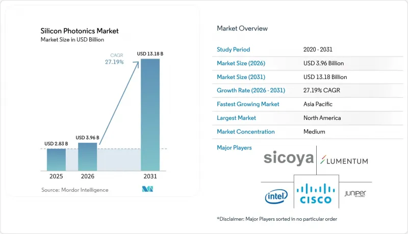
根據 Mordor Intelligence 預測,矽光電市場規模將從 2025 年的 28.3 億美元和 2026 年的 39.6 億美元成長到 2031 年的 131.8 億美元,2026 年至 2031 年的年複合成長率(CAGR)為 27.19%。
本報告按產品(例如光開關)、組件(主動式元件、被動元件)、晶圓尺寸(例如 300 毫米、200 毫米)、資料速率(例如 200 Gbps、400 Gbps)、應用(例如通訊、量子運算)、最終用戶(例如超大規模雲端供應商、通訊業者)和地區進行細分。市場預測以美元計價。
全球矽光電市場趨勢與洞察
在超大規模資料中心採用節能型共封裝光學元件
目前,光子晶片透過鍵合技術整合到交換器的矽晶片上,消除了插入式光學模組帶來的散熱問題,並釋放了寶貴的面板空間。 Marvell 的 51.2 Tbps 平台採用微環調製器,實現了每通道 200 Gbps 的傳輸速率,從而將交換器的功耗降低了約 30%。 NVIDIA 和台積電 (TSMC) 正在使用先進的中介層在 GPU 晶片之間路由光訊號,突破了 224 Gbps 的電頻寬限制。 Fabrinet 已投資 1.325 億美元擴大了其光學模組產能,以滿足市場對共封裝光元件的激增需求。儘管光網際網路論壇 (IOF) 已發布了指導草案,但各超大規模資料中心超大規模資料中心業者仍在繼續追求各自的封裝尺寸,導致供應鏈分散,供應商認證流程也更加複雜。
為促進低功耗光連接模組承擔的碳排放減少義務
預計到2024年,資料中心的電力消耗量將達到460太瓦時(TWh),全球監管機構正收緊電力使用限制。矽光電降低了互連的能耗,從而可以實現更高密度的機架配置和更高的進氣溫度。國際能源總署(IEA)警告稱,如果不進行光技術升級,到2030年電力需求可能會翻倍。 Omdia預測,到2030年,主要用於人工智慧的資本投資將達到5,450億美元,其中大部分將用於節能鏈路。雖然光子晶片的製造過程能耗較高,但生命週期分析表明,在超大規模部署中,光技術仍然優於銅纜。
矽基基板高於 70 度C時的熱預算限制
環形共振器每攝氏度溫度變化會產生0.1奈米的漂移,這需要封閉回路型加熱器,並會增加模組的功耗。汽車環境溫度通常超過攝氏85度,因此需要高成本的冷卻措施,並降低功率等級。資料中心採用液體循環系統來解決這個問題,但額外的基礎設施會增加總擁有成本(TCO)。研究人員正在探索碳化矽和氮化鋁基基板,它們有望降低熱光係數,但商業性應用仍需數年時間。
細分市場分析
受400G和800G光學模組超大規模部署的推動,收發器預計將佔據矽光電市場最大佔有率,到2025年將達到47.64%。感測器雖然佔有率較小,但預計其複合年成長率將達到28.74%,成為成長最快的產品,這主要得益於FMCW雷射雷達和屈光生物感測技術的發展。許多交換機廠商正專注於板載雷射器,這意味著部分獨立收發器的出貨量可能會轉向ASIC封裝。主動式光纜正在解決人工智慧叢集無法使用笨重銅線的問題,但光開關仍受到其控制平面複雜性的限制。
生物感測和汽車應用的興起表明,整個光電產業正從通訊領域向多元化發展。 Aurora 的 FMCW 雷射雷達在 300 公尺的距離上實現了厘米級精度,這得益於晶圓級矽光電整合技術的支援。在製藥領域,諧振位移感測器無需使用螢光染料即可加速高通量檢測,為晶片供應商創造了新的授權收入機會。 DARPA 的 PIPES 計畫正在資助全光分封交換技術,這表明光路由器未來可能會徹底改變電子結構。
預計到2025年,主動元件將佔矽光電市場佔有率的58.91%,並將以27.56%的複合年成長率成長。由於矽的間接帶隙特性,雷射器仍然是成本最高的組件,因為需要鍵合III-V族放大層。近期實驗已在矽上實現了單片生長的量子點雷射器,這是一項突破性進展,如果實現商業化,將顯著降低組件成本。利用PAM4調變技術,調變器頻寬已達到每聲道200 Gbps,為即將推出的1.6 Tbps插件式元件的實現奠定了基礎。
被動元件至關重要,但其成長速度正在放緩。被動元件的良率取決於波導管粗糙度和對準公差,即使是單一缺陷也會影響晶片性能。 OIF提案的光柵耦合器規格標準化方案可望縮短迭代週期。隨著GPU供應商擴大採用共封裝光學元件,雷射安裝製程正從模組製造商轉移到OSAT供應商,從而有效地重組了供應鏈。
區域分析
預計到2025年,北美將佔據42.76%的市場佔有率,這得益於《晶片技術創新與創新法案》(CHIPS Act)的資金支持以及英特爾、思科和博通等垂直整合巨頭的存在。與超大規模客戶的現場對接能夠加快協作設計週期,而美國國防高級研究計劃局(DARPA)的津貼則推動了光子分組交換領域的研究與開發。儘管高昂的人事費用和冗長的許可流程可能會延緩晶圓廠的建設,但財政獎勵透過減輕企業的財務負擔,顯著緩解了這項挑戰。這些獎勵通常包括稅收減免、津貼和補貼,有助於抵消高營運成本和監管延誤的挑戰。
預計到2031年,亞太地區將以28.11%的複合年成長率實現最高成長。台積電的先進封裝技術使包含光電、邏輯和記憶體的晶片能夠共存於同一基板上,從而降低互連過程中的功耗。中國的「中國製造2025」計畫投入數十億美元用於晶圓廠建設,旨在實現供應鏈本地化並降低出口限制風險。日本在光技術領域的專長以及韓國的5G部署也支撐著市場需求。然而,地緣政治緊張局勢威脅著設備的跨境流動和智慧財產權的許可。
歐洲正受益於歐盟430億歐元的晶片法案,但成員國之間的分歧阻礙了其推廣。德國弗勞恩霍夫研究所正主導汽車LiDAR的整合,法國原子能委員會-萊蒂研究所則與代工廠合作建造試點生產線。汽車產業的碳排放法規和數據主權規則催生了對節能光電技術的需求,但不斷上漲的能源成本和人事費用正在削弱製造業的競爭力。中東、非洲和南美洲仍然是通訊骨幹領域的先驅,這主要是因為它們正在向400G升級邁進。
其他好處:
- Excel格式的市場預測(ME)表
- 3個月的分析師支持
目錄
第1章:引言
- 研究假設和市場定義
- 調查範圍
第2章:調查方法
第3章執行摘要
第4章 市場狀況
- 市場概覽
- 市場促進因素
- 在超大規模資料中心部署高效率共封裝光元件
- 為促進低功耗光連接模組承擔的碳排放減少義務
- 5G去程傳輸/回程傳輸升級正在推動對 400/800G 模組的需求。
- 基於FMCW矽光電的3級LiDAR項目,適用於汽車應用
- 用於量子技術和安全光電的國防預算
- 政府的半導體激勵政策正在推動光電製造地。
- 市場限制因素
- 矽基基板高於 70 度C時的熱預算限制
- 包裝缺乏標準化導致非經常性工程成本上升。
- 在波長大於 1.55 µm 的範圍內,InP 和聚合物光電面臨競爭。
- 由於 300 毫米光子代工廠產能不足,前置作業時間越來越長。
- 產業價值鏈分析
- 監理展望
- 技術展望
- 宏觀經濟因素對市場的影響
- 波特五力分析
第5章 市場規模與成長預測
- 依產品
- 光收發器
- 光開關
- 主動光纜(AOC)
- 矽光電感測器
- 晶圓級測試系統
- 多工器/解多工器
- 衰減器和調製器
- 其他產品
- 按組件
- 主動元件
- 雷射
- 數據機
- 檢測器
- 被動元件
- 波導
- 篩選
- 耦合器
- 其他被動部件
- 主動元件
- 按晶圓尺寸
- 300 mm
- 200 mm
- 150毫米或更小
- 按數據速率
- 超過 100 Gbps
- 200 Gbps
- 400 Gbps
- 800 Gbps800 Gbps
- 超過 1.6 Tbps
- 透過使用
- 資料中心和高效能運算
- 電訊
- 汽車和自動駕駛汽車
- AR/VR 和家用電子電器
- 醫療保健和生命科學
- 國防/航太
- 量子計算
- 其他用途
- 最終用戶
- 超大規模雲端供應商
- 通訊業者
- 汽車製造商和一級供應商
- 醫療設備製造商
- 政府和國防機構
- 研究和學術機構
- 按地區
- 北美洲
- 美國
- 加拿大
- 墨西哥
- 歐洲
- 德國
- 英國
- 法國
- 義大利
- 其他歐洲國家
- 亞太地區
- 中國
- 日本
- 印度
- 韓國
- 澳洲
- 其他亞太國家
- 中東和非洲
- 中東
- 沙烏地阿拉伯
- 阿拉伯聯合大公國
- 其他中東國家
- 非洲
- 南非
- 埃及
- 其他非洲國家
- 中東
- 南美洲
- 巴西
- 阿根廷
- 其他南美國家
- 北美洲
第6章 競爭情勢
- 市場集中度
- 策略趨勢
- 市佔率分析
- 公司簡介
- Intel Corporation
- Cisco Systems Inc.
- Broadcom Inc.
- Lumentum Holdings Inc.
- Juniper Networks Inc.
- GlobalFoundries Inc.
- Sicoya GmbH
- Molex LLC
- Marvell Technology Inc.
- MACOM Technology Solutions
- Coherent Corp.
- Hamamatsu Photonics KK
- Ayar Labs Inc.
- NeoPhotonics Corp.
- IBM Corporation
- Hewlett Packard Enterprise Company
- Coherent Corp.
- Rockley Photonics
- Infinera Corporation
- Smart Photonics
- DustPhotonics Inc.
- PsiQuantum, Corp.
- POET Technologies
- Tower Semiconductor Ltd.
第7章 市場機會與未來展望
According to Mordor Intelligence, the silicon photonics market size is projected to expand from USD 2.83 billion in 2025 and USD 3.96 billion in 2026 to USD 13.18 billion by 2031, registering a CAGR of 27.19% between 2026 to 2031.
This report is Segmented by Product (Optical Switches, and More), Component (Active Components, and Passive Components), Wafer Size (300 Mm, 200 Mm, and More), Data Rate (200 Gbps, 400 Gbps, and More), Application (Telecommunications, Quantum Computing, and More), End-User (Hyperscale Cloud Providers, Telecom Operators, and More), and Geography. The Market Forecasts are Provided in Terms of Value (USD).
Global Silicon Photonics Market Trends and Insights
Energy-Efficient Co-Packaged Optics Adoption in Hyperscale Data Centers
Photonic dies are now bonded to switch silicon, removing the thermal penalties of pluggable optics and freeing valuable faceplate real estate. Marvell's 51.2 Tbps platform employs micro-ring modulators delivering 200 Gbps per lane, lowering switch power by roughly 30%. NVIDIA and TSMC use advanced interposers to route optical signals among GPU chiplets, overcoming the electrical bandwidth ceiling at 224 Gbps. Fabrinet expanded its optical module capacity by USD 132.5 million to meet swelling demand for co-packaged optics. Although the Optical Internetworking Forum released draft guidance, each hyperscaler continues to pursue proprietary form factors, fragmenting supply and complicating vendor qualification.
Carbon-Reduction Mandates Driving Low-Power Optical Interconnects
Global regulators are tightening power-use limits amid data centers' 460 TWh consumption in 2024. Silicon photonics reduces interconnect energy consumption, enabling denser racks and higher inlet temperatures. The International Energy Agency warns electricity demand could double by 2030 without optical upgrades. Omdia forecasts USD 545 billion in AI-centric capital outlays by 2030, much of it channeled to energy-efficient links. Although photonic chip fabrication is energy-intensive, lifecycle analyses still favor optics over copper for hyperscale deployments.
Thermal Budget Limitations in Silicon Substrates Above 70 °C
Ring resonators drift 0.1 nm per °C, forcing closed-loop heaters and raising module power. Automotive ambient temperatures often exceed 85 °C, demanding costly cooling or derating. Data centers mitigate with liquid loops, yet added infrastructure inflates TCO. Researchers are exploring silicon carbide and aluminum nitride substrates to potentially reduce thermo-optic coefficients, yet widespread commercial adoption is still years off.
Other drivers and restraints analyzed in the detailed report include:
- 5G Fronthaul/Backhaul Upgrade Fueling 400 G and 800 G Modules
- Automotive Level-3 LiDAR Programs Leveraging FMCW Silicon Photonics
- Lack of Standardized Packaging Elevating NRE Costs
For complete list of drivers and restraints, kindly check the Table Of Contents.
Segment Analysis
Transceivers accounted for the largest share of the silicon photonics market, holding 47.64% in 2025, propelled by hyperscale adoption of 400 G and 800 G optics. Sensors, while smaller, will post the fastest 28.74% CAGR thanks to FMCW LiDAR and refractive index biosensing. Many switch vendors are eyeing on-board lasers, suggesting some standalone transceiver volumes may migrate onto ASIC packages. Active optical cables cater to AI clusters that cannot tolerate the bulk of copper, while optical switches remain hampered by control-plane complexity.
The rise of biosensing and automotive applications signals diversification across the Photonics industry beyond telecom. Aurora's FMCW LiDAR showcases centimeter-level accuracy at 300 m range, a feat that relies on wafer-scale silicon photonics integration. In pharma, resonant-shift sensors speed high-throughput assays without fluorescent dyes, opening new licensing revenue for chip suppliers. DARPA's PIPES program is funding all-optical packet switching, suggesting optical routers could eventually disrupt electrical fabrics.
Active devices accounted for 58.91% of the silicon photonics market share in 2025 and are projected to expand at a 27.56% CAGR. Lasers remain the costliest part because silicon's indirect bandgap necessitates bonded III-V gain layers. Recent lab work demonstrated quantum-dot lasers monolithically grown on silicon, a leap that could slash the bill of materials once commercialized. Modulator bandwidth has climbed to 200 Gbps per lane using PAM4, enabling upcoming 1.6 Tbps pluggables.
Passive components, while essential, are witnessing a slower growth trajectory. Their yield is contingent on waveguide roughness and alignment tolerances, where even a single defect can jeopardize die performance. Proposals by OIF to standardize grating-coupler specifications could potentially reduce iteration cycles. With GPU vendors increasingly adopting co-packaged optics, the laser attachment process is transitioning from module houses to OSAT providers, effectively reshaping the supply chain landscape.
Complete Report Scope:
- By Product
- Optical Transceivers
- Optical Switches
- Active Optical Cables (AOCs)
- Silicon Photonic Sensors
- Wafer-Level Test Systems
- Multiplexers/De-Multiplexers
- Attenuators and Modulators
- Other Products
- By Component
- Active Components
- Lasers
- Modulators
- Photodetectors
- Passive Components
- Waveguides
- Filters
- Couplers
- Other Passive Components
- Active Components
- By Wafer Size
- 300 mm
- 200 mm
- 150 mm and Below
- By Data Rate
- Above 100 Gbps
- 200 Gbps
- 400 Gbps
- 800 Gbps
- Above 1.6 Tbps
- By Application
- Data Centers and High-Performance Computing
- Telecommunications
- Automotive and Autonomous Vehicles
- AR/VR and Consumer Electronics
- Healthcare and Life Sciences
- Defense and Aerospace
- Quantum Computing
- Other Applications
- By End-User
- Hyperscale Cloud Providers
- Telecom Operators
- Automotive OEMs and Tier-1 Suppliers
- Medical Device Manufacturers
- Government and Defense Agencies
- Research and Academic Institutions
- By Geography
- North America
- United States
- Canada
- Mexico
- Europe
- Germany
- United Kingdom
- France
- Italy
- Rest of Europe
- Asia-Pacific
- China
- Japan
- India
- South Korea
- Australia
- Rest of Asia-Pacific
- Middle East and Africa
- Middle East
- Saudi Arabia
- United Arab Emirates
- Rest of Middle East
- Africa
- South Africa
- Egypt
- Rest of Africa
- Middle East
- South America
- Brazil
- Argentina
- Rest of South America
- North America
Geography Analysis
North America held a 42.76% share in 2025, buoyed by CHIPS Act funding and vertically integrated giants such as Intel, Cisco, and Broadcom. Local access to hyperscale customers enables fast co-design cycles, while DARPA grants spur photonic packet-switching R&D. While high labor costs and lengthy permitting processes can delay fab builds, fiscal incentives significantly alleviate this burden by reducing the financial strain on companies. These incentives often include tax breaks, grants, and subsidies, which help offset the challenges associated with high operational expenses and regulatory delays.
Asia-Pacific will post the quickest 28.11% CAGR through 2031. TSMC's advanced packaging nodes enable chiplets containing photonics, logic, and memory to coexist on a single substrate, reducing interconnect power consumption. China's Made in China 2025 plan allocates billions to fab construction, aiming to localize supply and mitigate export-control risk. Japan's optics expertise and Korea's 5G rollouts also underpin demand. Geopolitical frictions, however, threaten cross-border equipment flows and IP licensing.
Europe benefits from the EUR 43 billion EU Chips Act, yet fragmentation across member states impedes scale. Germany's Fraunhofer institutes lead automotive LiDAR integration, while France's CEA-Leti partners with foundries to build pilot lines. Automotive carbon mandates and data-sovereignty rules create pull for energy-efficient photonics, although higher energy and labor costs erode manufacturing competitiveness. The Middle East and Africa, plus South America, remain early adopters, chiefly in telecom backbones upgrading to 400 G.
- Intel Corporation
- Cisco Systems Inc.
- Broadcom Inc.
- Lumentum Holdings Inc.
- Juniper Networks Inc.
- GlobalFoundries Inc.
- Sicoya GmbH
- Molex LLC
- Marvell Technology Inc.
- MACOM Technology Solutions
- Coherent Corp.
- Hamamatsu Photonics K.K.
- Ayar Labs Inc.
- NeoPhotonics Corp.
- IBM Corporation
- Hewlett Packard Enterprise Company
- Coherent Corp.
- Rockley Photonics
- Infinera Corporation
- Smart Photonics
- DustPhotonics Inc.
- PsiQuantum, Corp.
- POET Technologies
- Tower Semiconductor Ltd.
Additional Benefits:
- The market estimate (ME) sheet in Excel format
- 3 months of analyst support
TABLE OF CONTENTS
1 INTRODUCTION
- 1.1 Study Assumptions and Market Definition
- 1.2 Scope of the Study
2 RESEARCH METHODOLOGY
3 EXECUTIVE SUMMARY
4 MARKET LANDSCAPE
- 4.1 Market Overview
- 4.2 Market Drivers
- 4.2.1 Energy-Efficient Co-Packaged Optics Adoption in Hyperscale Data Centers
- 4.2.2 Carbon-Reduction Mandates Driving Low-Power Optical Interconnects
- 4.2.3 5G Fronthaul/Backhaul Upgrade Fueling 400/800 G Modules
- 4.2.4 Automotive Level-3 LiDAR Programs Leveraging FMCW Silicon Photonics
- 4.2.5 Defense Funding for Quantum and Secure Photonics
- 4.2.6 Government Semiconductor Incentive Schemes Expanding Photonic Fabs
- 4.3 Market Restraints
- 4.3.1 Thermal Budget Limitations in Silicon Substrates Above 70 °C
- 4.3.2 Lack of Standardized Packaging Elevating NRE Costs
- 4.3.3 Competition from InP and Polymer Photonics Beyond 1.55 µm
- 4.3.4 Limited 300 mm Photonic Foundry Capacity Causing Extended Lead Times
- 4.4 Industry Value Chain Analysis
- 4.5 Regulatory Outlook
- 4.6 Technological Outlook
- 4.7 Impact of Macroeconomic Factors on the Market
- 4.8 Porter's Five Forces Analysis
- 4.8.1 Bargaining Power of Suppliers
- 4.8.2 Bargaining Power of Buyers
- 4.8.3 Threat of New Entrants
- 4.8.4 Threat of Substitutes
- 4.8.5 Intensity of Competitive Rivalry
5 MARKET SIZE AND GROWTH FORECASTS (VALUE)
- 5.1 By Product
- 5.1.1 Optical Transceivers
- 5.1.2 Optical Switches
- 5.1.3 Active Optical Cables (AOCs)
- 5.1.4 Silicon Photonic Sensors
- 5.1.5 Wafer-Level Test Systems
- 5.1.6 Multiplexers/De-Multiplexers
- 5.1.7 Attenuators and Modulators
- 5.1.8 Other Products
- 5.2 By Component
- 5.2.1 Active Components
- 5.2.1.1 Lasers
- 5.2.1.2 Modulators
- 5.2.1.3 Photodetectors
- 5.2.2 Passive Components
- 5.2.2.1 Waveguides
- 5.2.2.2 Filters
- 5.2.2.3 Couplers
- 5.2.2.4 Other Passive Components
- 5.2.1 Active Components
- 5.3 By Wafer Size
- 5.3.1 300 mm
- 5.3.2 200 mm
- 5.3.3 150 mm and Below
- 5.4 By Data Rate
- 5.4.1 Above 100 Gbps
- 5.4.2 200 Gbps
- 5.4.3 400 Gbps
- 5.4.4 800 Gbps
- 5.4.5 Above 1.6 Tbps
- 5.5 By Application
- 5.5.1 Data Centers and High-Performance Computing
- 5.5.2 Telecommunications
- 5.5.3 Automotive and Autonomous Vehicles
- 5.5.4 AR/VR and Consumer Electronics
- 5.5.5 Healthcare and Life Sciences
- 5.5.6 Defense and Aerospace
- 5.5.7 Quantum Computing
- 5.5.8 Other Applications
- 5.6 By End-User
- 5.6.1 Hyperscale Cloud Providers
- 5.6.2 Telecom Operators
- 5.6.3 Automotive OEMs and Tier-1 Suppliers
- 5.6.4 Medical Device Manufacturers
- 5.6.5 Government and Defense Agencies
- 5.6.6 Research and Academic Institutions
- 5.7 By Geography
- 5.7.1 North America
- 5.7.1.1 United States
- 5.7.1.2 Canada
- 5.7.1.3 Mexico
- 5.7.2 Europe
- 5.7.2.1 Germany
- 5.7.2.2 United Kingdom
- 5.7.2.3 France
- 5.7.2.4 Italy
- 5.7.2.5 Rest of Europe
- 5.7.3 Asia-Pacific
- 5.7.3.1 China
- 5.7.3.2 Japan
- 5.7.3.3 India
- 5.7.3.4 South Korea
- 5.7.3.5 Australia
- 5.7.3.6 Rest of Asia-Pacific
- 5.7.4 Middle East and Africa
- 5.7.4.1 Middle East
- 5.7.4.1.1 Saudi Arabia
- 5.7.4.1.2 United Arab Emirates
- 5.7.4.1.3 Rest of Middle East
- 5.7.4.2 Africa
- 5.7.4.2.1 South Africa
- 5.7.4.2.2 Egypt
- 5.7.4.2.3 Rest of Africa
- 5.7.4.1 Middle East
- 5.7.5 South America
- 5.7.5.1 Brazil
- 5.7.5.2 Argentina
- 5.7.5.3 Rest of South America
- 5.7.1 North America
6 COMPETITIVE LANDSCAPE
- 6.1 Market Concentration
- 6.2 Strategic Moves
- 6.3 Market Share Analysis
- 6.4 Company Profiles (includes Global level Overview, Market level overview, Core Segments, Financials as available, Strategic Information, Market Rank/Share for key companies, Products and Services, and Recent Developments)
- 6.4.1 Intel Corporation
- 6.4.2 Cisco Systems Inc.
- 6.4.3 Broadcom Inc.
- 6.4.4 Lumentum Holdings Inc.
- 6.4.5 Juniper Networks Inc.
- 6.4.6 GlobalFoundries Inc.
- 6.4.7 Sicoya GmbH
- 6.4.8 Molex LLC
- 6.4.9 Marvell Technology Inc.
- 6.4.10 MACOM Technology Solutions
- 6.4.11 Coherent Corp.
- 6.4.12 Hamamatsu Photonics K.K.
- 6.4.13 Ayar Labs Inc.
- 6.4.14 NeoPhotonics Corp.
- 6.4.15 IBM Corporation
- 6.4.16 Hewlett Packard Enterprise Company
- 6.4.17 Coherent Corp.
- 6.4.18 Rockley Photonics
- 6.4.19 Infinera Corporation
- 6.4.20 Smart Photonics
- 6.4.21 DustPhotonics Inc.
- 6.4.22 PsiQuantum, Corp.
- 6.4.23 POET Technologies
- 6.4.24 Tower Semiconductor Ltd.
7 MARKET OPPORTUNITIES AND FUTURE OUTLOOK
- 7.1 White-space and Unmet-Need Assessment

 全球光電封裝市場(2027-2037 年)
 矽光電市場:2026-2032年全球市場預測(依產品類型、組件、封裝類型、材料類型、整合類型、最終用途及應用分類)全球矽光電、LPO/LRO 和 NPO/CPO 市場(2027-2037 年)
 矽光電市場:按產品、組件、材料、晶圓尺寸、資料速率、應用和最終用戶產業分類-市場規模、產業動態、機會分析和預測(2026-2035 年)
 矽光電市場預測至2034年-按組件、產品類型、應用、終端用戶產業和地區分類的全球分析
 2035 年前人工智慧資料中心矽光電市場分析和預測:按類型、產品類型、服務、技術、組件、應用、材料類型、設備、最終用戶和功能分類。全球矽光子和光子積體電路市場(2026-2036 年)
 矽光電市場-全球產業規模、佔有率、趨勢、機會、預測:按組件、應用、波導管、產品、材料、地區和競爭對手分類,2021-2031年
 矽光電市場:按應用和地區分類
 2026年III-V族矽光電全球市場報告