


 |
市場調查報告書
商品編碼
2063932
中國LED外延片:市佔率分析、產業趨勢與統計及成長預測(2026-2031年)China LED Epitaxial Wafer - Market Share Analysis, Industry Trends & Statistics, Growth Forecasts (2026 - 2031) |
||||||
※ 本網頁內容可能與最新版本有所差異。詳細情況請與我們聯繫。
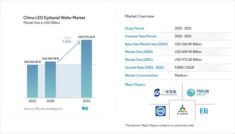
根據 Mordor Intelligence 預測,中國 LED 外延片市場規模預計到 2025 年將達到 5.648 億美元,到 2026 年將達到 6.099 億美元,到 2031 年將達到 9.733 億美元。
預計從 2026 年到 2031 年,其複合年成長率將達到 9.8%。
本報告依據材料系統(GaN基外延晶片、AlInGaP外延晶片等)、基板類型(藍寶石、矽、碳化矽(SiC)、砷化鎵(GaAs))、晶片直徑(100mm及以下、150mm、200mm及以上)及應用(通用照明、汽車照明、通用照明、汽車照明、顯示器及背光等)進行分類。市場預測以美元(USD)計價。
中國LED外延片市場的趨勢與洞察
政府對國內LED供應鏈的補貼與稅收優惠
「十四五」規劃優先扶持先進製程節點,而非單純追求產能擴張,使200mm氮化鎵矽基(GaN-on-Si)和鋁氮化鎵(AlGaN)反應器的有效資本成本降低了高達30%。廈門和武漢的省級項目結合了免費土地供應和公用事業收費折扣,使營運成本降低了10-15%,加快了新建晶圓廠的損益平衡點。目前,政府已設定目標,到2027年國產設備的採用率要達到70%,這將使訂單集中流向AMEC等本土MOCVD供應商,並保護其戰略技術訣竅。這些政策組合縮短了投資回收期,在晶片利潤率下降的情況下維持了研發投入,並為2031年前擴大優質晶圓生產奠定了堅實的基礎。
提高能源效率的法規促進了LED在一般照明中的應用。
中國的碳中和承諾為建築維修提供了結構性支撐。 GB 50034-2024標準將最低光通量效率標準提高到110-130 lm/W,使得傳統螢光具的效率無法衡量,並強制要求政府設施維修。地方政府補貼計畫可報銷高達40%的維修費用,加快了更換週期,即使在商品化進程中也能維持基準貨量。智慧住宅燈泡的普及進一步推動了需求,因為可調光白光照明解決方案需要雙晶片或RGB晶圓。這些因素表明,即使資本投資轉向顯示器和汽車產業,中國LED外延晶圓市場仍將繼續受益於照明產業的穩定需求。
迷你和微型LED顯示器生產線的快速擴張
各大顯示器廠商正透過將晶圓供應與面板藍圖直接掛鉤,並簽訂長期起步協議,將其6吋和200mm的產能轉向RGB和高均勻性藍色產品。 TCL華星光電收購Prima,確保了後端整合,並為符合3nm以下波長目標的晶圓創造了穩定的需求。三安半導體在2024年至2025年間將其microLED晶圓月產量提高了五倍以上,達到了三星旗艦電視的採用標準,並證明了中國廠商能夠達到高階均勻性標準。華芯電子珠海工廠的6吋晶圓月產量增加了3000片,以配合京東方對8.6代背光技術的30億美元投資。這些措施將為中期成長奠定基礎,提高關鍵晶圓廠的產運轉率,並消化通用照明生產線的過剩產能。
細分市場分析
2025年,氮化鎵(GaN)基晶圓將佔據市場價值的65%,其應用領域涵蓋磷光體轉換白光燈、RGB背光燈以及汽車頭燈的藍光發射。照明和顯示產業的穩定供應確保了該領域持續的現金流,從而推動了研發投入。儘管AlGaN目前僅佔總產量的一小部分,但預計其複合年成長率將達到12.34%,顯著超過中國整體LED外延晶圓市場,這主要得益於醫療法規禁止使用汞燈以及對現場消毒需求的不斷成長。三安半導體投資9.5億美元進行多年擴建,以及湖北杜維特半導體一條中試生產線的運作,顯示中國正致力於取代進口,主導深紫外線(DUV)價值鏈。 AlInGaP輔助生產線則為汽車煞車燈和園藝產業提供產品,為高性能晶圓廠抵禦市場波動提供了保障。
晶圓級AlGaN的市場接受度得益於近期技術突破,其外量子效率已提升至近10%,為東南亞供水事業開闢了出口前景。國內市政競標中對固體UVC技術日益重視,也確保了永續的需求的基礎。 GaN的優勢與AlGaN的成長相結合,共同作用,穩定了收益,使中國LED外延晶圓市場能夠在不影響短期回報的前提下,投資於製程創新。
預計到2025年,藍寶石將佔據55.63%的市場佔有率,這主要得益於其晶格一致性、成熟的8英寸供應鏈以及與汽車OEM廠商的親和性。其久經考驗的可靠性確保了其在車頭燈和戶外照明燈具領域的持續應用,即使在照明行業價格壓力不斷增加的情況下也是如此。矽基氮化鎵(GaN)具有直徑達200毫米的大尺寸、更低的原料成本以及與現有CMOS晶圓廠的兼容性,因此對藍寶石構成了強力的挑戰,其複合年成長率(CAGR)高達13.3%,超過了藍寶石的成長率。在中國LED外延晶片市場,矽基氮化鎵的佔有率成長最為迅速,尤其是在面板製造商尋求降低元件成本的領域,例如mini-LED背光。
工藝成熟度仍然是一大障礙。 200mm氮化鎵矽基元件的邊緣相關正向電壓漂移仍會減少可用晶片面積,但像ALLOS和Ennostar這樣的合作有望實現低於3%的波長均勻性。這將是實現大規模重複利用而無需分級的閾值。碳化矽將服務於特定的功率和高溫應用,與電動車動力系統的逆變器重疊,並且相互利用晶體生長技術具有優勢。因此,基板結構正在向雙軌結構演進,藍寶石用於保護需要高可靠性的市場,而矽則滿足大規模生產的消費顯示器的需求。
其他好處:
- Excel格式的市場預測(ME)表
- 3個月的分析師支持
目錄
第1章:引言
- 研究假設和市場定義
- 調查範圍
第2章:調查方法
第3章執行摘要
第4章 市場狀況
- 市場概覽
- 市場促進因素
- 迷你和微型LED顯示器生產線快速擴張
- 政府對國內LED供應鏈的補貼與稅收優惠
- 提高能源效率的法規旨在鼓勵一般照明中廣泛採用LED。
- 加速新能源車中汽車LED的採用
- 水處理領域對UVC LED外延晶片的需求不斷成長。
- 促進本地化以穩定碳化矽基板的供應。
- 市場限制因素
- MOCVD設備的高資本密集度和折舊免稅額
- 由於傳統LED晶片供應過剩,價格下降
- 200 毫米 GaN-on-Si 平台良率相關的技術挑戰
- 有關氨和砷排放的環境法規限制了企業擴張。
- 產業價值鏈分析
- 監理情勢
- 技術展望
- 宏觀經濟因素對市場的影響
- 波特五力分析
第5章 市場規模與成長預測
- 材料
- 基於氮化鎵的外延晶片
- AlInGaP外延晶片
- AlGaN外延晶片
- 依基材類型
- 藍寶石
- 矽
- 碳化矽(SiC)
- 砷化鎵(GaAs)
- 依晶圓直徑
- 100毫米或更小
- 150 mm
- 200毫米或以上
- 透過使用
- 一般照明
- 汽車照明
- 顯示器和背光
- 紫外線消毒
- 工業和專用照明
第6章 競爭情勢
- 市場集中度
- 策略趨勢
- Vendor Market Positioning
- 公司簡介
- Sanan Optoelectronics Co., Ltd.
- HC Semitek Corporation
- Focus Lightings Tech Co., Ltd.
- Elec-Tech International Co., Ltd.
- NationStar Optoelectronics Co., Ltd.
- Epistar Corporation
- Osram Opto Semiconductors GmbH
- Cree LED(Smart Global Holdings, Inc.)
- Seoul Semiconductor Co., Ltd.
- Genesis Photonics Inc.
- Changelight Co., Ltd.
- Epileds Technologies Inc.
- Opto Tech Corporation
- Aucksun Crystal
- EpiWorld International Co., Ltd.
- SinoNitride Semiconductor Co., Ltd.
- Advanced Epitaxy Technology Inc.
- Lextar Electronics Corp.
- Nichia Corporation
- Hangzhou Silan Microelectronics Co., Ltd.
第7章 市場機會與未來展望
According to Mordor Intelligence, the china lED epitaxial wafer market size is projected to be USD 564.8 million in 2025, USD 609.9 million in 2026, and reach USD 973.3 million by 2031, growing at a CAGR of 9.8% from 2026 to 2031.
This report is Segmented by Material System (GaN-Based Epitaxial Wafers, Alingap Epitaxial Wafers, and More), Substrate Type (Sapphire, Silicon, Silicon Carbide (SiC), Gallium Arsenide (GaAs)), Wafer Diameter (Up To 100 Mm, 150 Mm, 200 Mm and Above), and Application (General Lighting, Automotive Lighting, Displays and Backlighting and More). The Market Forecasts are Provided in Terms of Value (USD).
China LED Epitaxial Wafer Market Trends and Insights
Government Subsidies And Tax Incentives For Domestic LED Supply Chain
The 14th Five-Year Plan tilts subsidies toward advanced nodes rather than sheer volume, cutting effective capital costs for 200 mm GaN-on-Si and AlGaN reactors by up to 30%. Provincial programs in Xiamen and Wuhan layer land concessions and utility discounts that shave operating expenses by 10-15%, accelerating breakeven for new fabs. Conditions now require 70% domestic equipment content by 2027, funneling orders to local MOCVD vendors such as AMEC and protecting strategic know-how. The policy mix reduces payback periods, sustains R&D outlays despite thinning chip margins, and lengthens the runway for premium-grade wafer expansion through 2031.
Energy Efficiency Mandates Driving LED Adoption In General Lighting
China's carbon-neutral pledge turns building retrofits into a structural floor of demand. Standard GB 50034-2024 lifts minimum efficacy thresholds to 110-130 lm/W, rendering legacy fluorescent fixtures non-compliant and triggering mandated upgrades in government facilities.Municipal rebates reimburse up to 40% of retrofit costs, bringing forward replacement cycles and sustaining baseline wafer shipments even amid commoditization. Residential smart bulbs add incremental pull by requiring dual-chip or RGB wafers for tunable white solutions. This driver ensures the China LED epitaxial wafer market continues to harvest steady lighting demand while shifting capex toward display and vehicle segments.
Rapid Expansion Of Mini And Micro LED Display Manufacturing Lines
Display giants are tying wafer supply directly to panel roadmaps, locking in long-term offtake agreements that pull 6-inch and 200 mm capacity toward RGB and high-uniformity blue products. TCL CSOT's acquisition of Prima secures back-end integration and creates stable demand for wafers that meet sub-3 nm wavelength targets.Sanan more than quintupled monthly microLED wafer output across 2024-2025, qualifying for Samsung's flagship televisions and proving Chinese vendors can hit premium uniformity benchmarks. HC Semitek's Zhuhai fab adds 3,000 six-inch wafers a month of incremental volume, synchronized with BOE's USD 3 billion Gen 8.6 backlight investments. Together, these moves anchor medium-term growth, lifting utilization at leading fabs and absorbing oversupply from general-lighting lines.
Other drivers and restraints analyzed in the detailed report include:
- Accelerated Automotive LED Penetration In New Energy Vehicles
- Price Erosion Due To Overcapacity In Conventional LED Chips
- High Capital Intensity And Depreciation Of MOCVD Equipment
For complete list of drivers and restraints, kindly check the Table Of Contents.
Segment Analysis
GaN-based wafers captured 65% of the 2025 value, underpinned by blue emission for phosphor-converted white lamps, RGB backlights, and automotive headlamps. Stable volumes from lighting and displays mean this segment continues to anchor cash flow and subsidize R&D. AlGaN supplies only a fraction of present output, yet health-sector regulations banning mercury lamps and rising demand for point-of-use sterilization enable a 12.34% CAGR that materially outpaces the China LED epitaxial wafer market size as a whole. Sanan's USD 950 million multiyear build-out, plus pilot lines at Hubei DUVTek, signal that China aims to displace imports and own the deep-UV value chain. Secondary AlInGaP lines serve automotive brake lights and horticulture, giving fabs a hedge against blue-chip cyclicality.
Commercial acceptance of wafer-scale AlGaN rides on recent breakthroughs pushing external quantum efficiency near 10%, opening export prospects to Southeast Asian water utilities. Domestic municipal tenders increasingly stipulate solid-state UVC, locking in a durable demand baseline. Taken together, the portfolio effect of GaN dominance and AlGaN growth stabilizes revenue, ensuring the China LED epitaxial wafer market can bankroll process innovations without jeopardizing near-term earnings.
Sapphire commanded a 55.63% share in 2025 thanks to lattice compatibility, an established 8-inch supply, and familiarity among automotive OEMs. Its proven reliability preserves design-in status for headlamps and outdoor fixtures even as price pressure mounts in lighting. Silicon-based GaN is the natural challenger, offering a larger 200 mm diameter, lower raw-wafer cost, and compatibility with existing CMOS fabs, underpinning a 13.3% CAGR that overtakes sapphire growth. The China LED epitaxial wafer market share for silicon rises fastest where panel makers chase bill-of-materials savings, particularly in mini-LED backlighting.
Process maturity remains the gating factor. Edge-related forward-voltage drift on 200 mm GaN-on-Si still reduces usable die area, but partnerships such as ALLOS-Ennostar promise sub-3% wavelength uniformity, a threshold that unlocks bin-free mass transfer. Silicon carbide fills niche power and high-temperature roles, overlapping with EV drive-train inverters and offering cross-utilization of crystal growth know-how. The substrate mix therefore evolves toward a dual-track structure, with sapphire safeguarding stringent reliability markets and silicon harvesting high-volume consumer displays.
List of Companies Covered in this Report:
- Sanan Optoelectronics Co., Ltd.
- HC Semitek Corporation
- Focus Lightings Tech Co., Ltd.
- Elec-Tech International Co., Ltd.
- NationStar Optoelectronics Co., Ltd.
- Epistar Corporation
- Osram Opto Semiconductors GmbH
- Cree LED (Smart Global Holdings, Inc.)
- Seoul Semiconductor Co., Ltd.
- Genesis Photonics Inc.
- Changelight Co., Ltd.
- Epileds Technologies Inc.
- Opto Tech Corporation
- Aucksun Crystal
- EpiWorld International Co., Ltd.
- SinoNitride Semiconductor Co., Ltd.
- Advanced Epitaxy Technology Inc.
- Lextar Electronics Corp.
- Nichia Corporation
- Hangzhou Silan Microelectronics Co., Ltd.
Additional Benefits:
- The market estimate (ME) sheet in Excel format
- 3 months of analyst support
TABLE OF CONTENTS
1 INTRODUCTION
- 1.1 Study Assumptions and Market Definition
- 1.2 Scope of the Study
2 RESEARCH METHODOLOGY
3 EXECUTIVE SUMMARY
4 MARKET LANDSCAPE
- 4.1 Market Overview
- 4.2 Market Drivers
- 4.2.1 Rapid Expansion of Mini and Micro LED Display Manufacturing Lines
- 4.2.2 Government Subsidies and Tax Incentives for Domestic LED Supply Chain
- 4.2.3 Energy Efficiency Mandates Driving LED Adoption in General Lighting
- 4.2.4 Accelerated Automotive LED Penetration in New Energy Vehicles
- 4.2.5 Rising Demand for UVC LED Epitaxial Wafers for Water Purification
- 4.2.6 Localization Push for Silicon Carbide Substrate Supply Security
- 4.3 Market Restraints
- 4.3.1 High Capital Intensity and Depreciation of MOCVD Equipment
- 4.3.2 Price Erosion Due to Overcapacity in Conventional LED Chips
- 4.3.3 Technical Yield Challenges in 200 mm GaN-on-Si Platforms
- 4.3.4 Environmental Regulations on Ammonia and Arsine Emissions Limiting Expansion
- 4.4 Industry Value Chain Analysis
- 4.5 Regulatory Landscape
- 4.6 Technological Outlook
- 4.7 Impact of Macroeconomic Factors on the Market
- 4.8 Porter's Five Forces Analysis
- 4.8.1 Bargaining Power of Suppliers
- 4.8.2 Bargaining Power of Buyers
- 4.8.3 Threat of New Entrants
- 4.8.4 Threat of Substitutes
- 4.8.5 Competitive Rivalry
5 MARKET SIZE AND GROWTH FORECASTS (VALUE)
- 5.1 By Material System
- 5.1.1 GaN-based Epitaxial Wafers
- 5.1.2 AlInGaP Epitaxial Wafers
- 5.1.3 AlGaN Epitaxial Wafers
- 5.2 By Substrate Type
- 5.2.1 Sapphire
- 5.2.2 Silicon
- 5.2.3 Silicon Carbide (SiC)
- 5.2.4 Gallium Arsenide (GaAs)
- 5.3 By Wafer Diameter
- 5.3.1 Up to 100 mm
- 5.3.2 150 mm
- 5.3.3 200 mm and Above
- 5.4 By Application
- 5.4.1 General Lighting
- 5.4.2 Automotive Lighting
- 5.4.3 Displays and Backlighting
- 5.4.4 UV Sterilization
- 5.4.5 Industrial and Specialty Lighting
6 COMPETITIVE LANDSCAPE
- 6.1 Market Concentration
- 6.2 Strategic Moves
- 6.3 Vendor Market Positioning
- 6.4 Company Profiles (includes Global Level Overview, Market Level Overview, Core Segments, Financials as available, Strategic Information, Market Rank/Share, Products and Services, Recent Developments)
- 6.4.1 Sanan Optoelectronics Co., Ltd.
- 6.4.2 HC Semitek Corporation
- 6.4.3 Focus Lightings Tech Co., Ltd.
- 6.4.4 Elec-Tech International Co., Ltd.
- 6.4.5 NationStar Optoelectronics Co., Ltd.
- 6.4.6 Epistar Corporation
- 6.4.7 Osram Opto Semiconductors GmbH
- 6.4.8 Cree LED (Smart Global Holdings, Inc.)
- 6.4.9 Seoul Semiconductor Co., Ltd.
- 6.4.10 Genesis Photonics Inc.
- 6.4.11 Changelight Co., Ltd.
- 6.4.12 Epileds Technologies Inc.
- 6.4.13 Opto Tech Corporation
- 6.4.14 Aucksun Crystal
- 6.4.15 EpiWorld International Co., Ltd.
- 6.4.16 SinoNitride Semiconductor Co., Ltd.
- 6.4.17 Advanced Epitaxy Technology Inc.
- 6.4.18 Lextar Electronics Corp.
- 6.4.19 Nichia Corporation
- 6.4.20 Hangzhou Silan Microelectronics Co., Ltd.
7 MARKET OPPORTUNITIES AND FUTURE OUTLOOK
- 7.1 White-space and Unmet-Need Assessment
 亞太地區LED外延片:市佔率分析、產業趨勢與統計及成長預測(2026-2031年)
 氮化鎵裝置市場預測至2034年-按產品類型、元件、電壓範圍、最終用戶和地區分類的全球分析氮化鎵基LED外延片:市佔率分析、產業趨勢與統計及成長預測(2026-2031年)氮化鎵矽基(GaN-on-Si)LED外延片:市佔率分析、產業趨勢與統計數據以及成長預測(2026-2031年)
 2026-2034年全球氮化鎵工業裝置市場規模、佔有率、趨勢與成長分析報告
 氮化鎵半導體裝置市場:2026-2032年全球市場預測(按裝置類型、晶圓尺寸、應用和最終用途產業分類)矽基基板的氮化鎵(GaN)晶圓:市佔率分析、產業趨勢與統計、成長預測(2026-2031)氮化鎵雷達系統市場:按類型、組件、頻寬、組件範圍和應用分類-2026年至2032年全球預測
 氮化鎵半導體市場:依產品、組件、晶圓尺寸、最終用途、國家及地區分類-全球產業分析、市場規模、市場佔有率及2025年至2032年預測
 高頻氮化鎵半導體市場分析及預測(至2035年):依類型、產品類型、服務、技術、應用、材料類型、裝置、部署類型、最終用戶和功能分類