


 |
市場調查報告書
商品編碼
2044055
氮化鎵基LED外延片:市佔率分析、產業趨勢與統計及成長預測(2026-2031年)GaN-Based LED Epitaxial Wafers - Market Share Analysis, Industry Trends & Statistics, Growth Forecasts (2026 - 2031) |
||||||
※ 本網頁內容可能與最新版本有所差異。詳細情況請與我們聯繫。
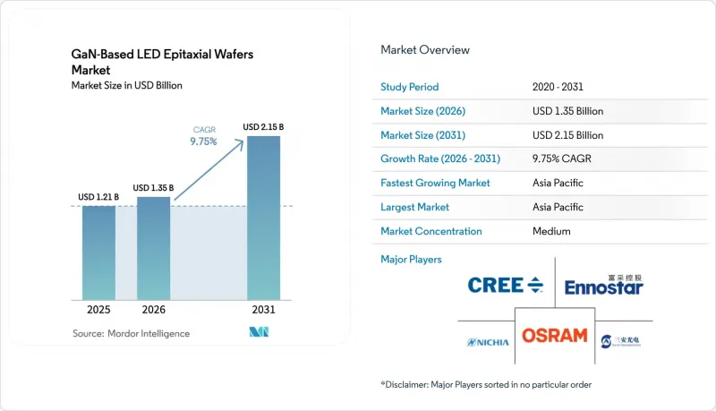
預計 GaN 基 LED 外延晶片市場將從 2026 年的 13.5 億美元成長到 2031 年的 21.5 億美元,2026 年至 2031 年的複合年成長率為 9.75%。
由於金屬有機化學氣相沉積 (MOCVD) 平台日益成熟、mini-LED 和 micro-LED 顯示器的快速普及以及 MOCVD 在電動車頭燈領域的應用日益廣泛,市場需求正在不斷成長。供應商正將其產能從通用照明晶圓轉向對波長均勻性和缺陷規格要求更高的高價值光電、感測和汽車基板。設備製造商在 200mm 和 300mm 規格的產品中展現出成本優勢,而亞太地區的垂直整合型企業則利用上游工程晶體生長控制和下游封裝技術來縮短開發週期。
全球氮化鎵基LED外延片市場趨勢及洞察
迷你LED和微型LED顯示器的快速普及
為了克服OLED燒屏難題並實現更高的峰值亮度,顯示器製造商正在加速推進Mini-LED和Micro-LED的研發,這導致對波長均勻性小於5nm、尺寸為200mm和300mm的基板的需求不斷成長。 Ennostar與ALLOS Semiconductors合作,宣布了一項用於穿戴式顯示器的200mm GaN-on-Si項目,該項目可實現超過2000 PPI的像素密度。蘋果已向位於新竹科學園區的友達光電和晶元光電投資3.34億美元,以確保未來穿戴式顯示器垂直整合的外延技術供應。 ams OSRAM的EVIYOS HD25模組(應用於蔚來ET9)也體現了與汽車產業的密切合作。該模組整合了25600個Micro-LED像素,需要採用顯示級外延技術才能實現500公尺的投影距離。
擴大電動車頭燈生產
電動車製造商正在指定使用像素超過10,000的自我調整頭燈,這就要求晶圓具備低缺陷、高亮度,並且能夠承受嚴格的AEC-Q測試循環。 EVIYOS HD25將投射距離從400米擴展到500米,並將中速行駛時的近光燈亮度提升了50%,這充分展現了晶圓性能的巨大飛躍。目前,高階電動車配備了超過100個LED構裝,每個封裝都採用外延材料,這些材料必須在較大的溫度波動範圍內保持色彩穩定性。
資本密集型MOCVD設備升級
最先進的300毫米GaN反應器單價超過500萬美元,但一個完整的生產群集需要8到10台設備,外加即時測量系統和機器人系統。 Veeco預測其Propel300的銷售額將在2026年達到8,000萬美元,這意味著目前只有極少數晶圓廠能夠消化如此龐大的資金。中小規模的外延晶圓供應商面臨策略困境。雖然他們傳統的150毫米和200毫米MOCVD設備已經完全折舊免稅額,並且可以以具有競爭力的現金成本生產晶圓,但這些平台無法與300毫米規格的「晶片/晶圓」經濟效益相媲美,而且隨著大型代工廠擴大規模,他們的利潤率將面臨壓力。
細分市場分析
到2025年,尺寸小於150mm的晶圓將佔總銷售額的68.71%,這反映了通用照明熱潮期間建造的傳統MOCVD工廠的規模。隨著代工廠追求晶片數量優勢和與矽CMOS生產線的兼容性,基於GaN的LED外延晶圓市場(300mm基板)預計將以10.89%的複合年成長率成長。在300mm生態系統日趨成熟之際,中等尺寸的200mm晶圓正在滿足當前顯示器背光的需求,Ennostar-ALLOS的微型LED穿戴式設備計畫就是一個典型的例子。向300mm晶圓的轉變將在功率和射頻領域最為顯著,因為在單一晶圓上整合GaN和CMOS驅動器可以減少模組尺寸並降低成本。然而,更大的直徑會加劇熱不均勻性,需要複雜的基板設計和即時溫度測量。
成本波動也波及上游。基板供應商現在必須提供符合更嚴格平整度和表面粗糙度規格的300毫米藍寶石和矽晶圓。 ROHM Semiconductor與台積電於2026年2月簽署的合作協議,旨在利用現有的300毫米潔淨室設施共同開發氮化鎵功率元件,凸顯了基礎設施共用的優勢。然而,由於高昂的資本投入和漫長的汽車行業認證流程,預計在預測期內,300毫米晶圓的廣泛應用仍將僅限於資金雄厚的晶圓廠。
預計到2025年,主要由mini-LED背光和通用照明驅動的光電產業將持續保持領先地位,佔44.28%的銷售額。然而,隨著垂直共振腔面射型雷射(VCSEL)和雷射雷達光源的普及,感測器產業預計將實現10.97%的複合年成長率。基於GaN的LED外延晶片在分離式功率元件領域的市佔率成長速度放緩,這主要是由於成本驅動的充電器應用領域,價格優先於缺陷密度。
感測器領域的快速成長反映了汽車安全法規強制要求配備先進駕駛輔助系統(ADAS) 與消費者對智慧型手機和穿戴式裝置臉部辨識和擴增實境(AR) 功能的需求之間的融合。微機電系統 (MEMS) 和微型光子元件等微型領域正崛起為極具潛力的成長點。儘管目前的產量有限,但基於氮化鎵 (GaN) 的共振器和光子積體電路在實現晶片級雷射雷達 (LiDAR) 方面的潛力,可能會催生對超低缺陷外延晶片的新需求。光電子裝置預計仍將佔據主導地位,但隨著感測需求的加速成長,其主導地位正在逐漸減弱。
區域分析
預計到2025年,亞太地區將佔全球銷售額的56.27%,並將以10.73%的複合年成長率成長,這主要得益於台灣垂直整合的叢集和中國大陸的產能擴張補貼政策。台灣企業如晶元光電(Epistar)、力士光電(Rexter)和恩諾斯達光電(Enostar)與面板組裝廠商緊密合作,加速了微型LED生產所需的回饋循環。主要企業三安光電(Sanan Optoelectronics)正積極擴大業務規模,這得益於政府獎勵以及其計劃收購Lumileds,旨在為歐美汽車行業拓展銷售管道。
北美和歐洲雖然需求佔有率較小,但卻扮演著重要的戰略角色。美國能源局(DOE) 的資金支持抵消了新型外延製造流程的初期風險,而歐洲汽車製造商則要求主動式轉向頭燈使用經 AEC-Q 認證的晶圓,這為本地供應商設定溢價創造了空間。技術流動是雙向的,凸顯了全球供應鏈的整合,例如歐洲的 LED 創新技術,如歐司朗 (ams OSRAM) 的 EVIYOS,正被應用於中國的電動車。
包括南美、中東和非洲在內的世界其他地區仍處於發展階段,照明和標誌設備依賴進口LED模組。然而,旨在建立國內半導體生產能力的政府項目預計將在長期內提振該地區的晶圓需求,尤其是在優先發展化合物半導體裝置以實現可再生能源和電信基礎設施目標的情況下。
其他好處:
- Excel格式的市場預測(ME)表
- 3個月的分析師支持
目錄
第1章:引言
- 研究假設和市場定義
- 調查範圍
第2章:調查方法
第3章執行摘要
第4章 市場狀況
- 市場概覽
- 市場促進因素
- 政府對固體照明計畫的補貼
- 迷你和微型LED顯示器的快速普及
- 擴大電動車頭燈生產
- 自主型GaN基板在缺陷減少的新應用
- 過渡到不含金(Au)的銅(Cu)基金屬化以降低成本。
- 用於垂直LED的現場再生技術
- 市場限制因素
- 資本密集型MOCVD設備升級
- 高純度藍寶石錠的供應波動
- 300毫米平台的溫度控管挑戰
- 圍繞圖案化藍寶石基板的知識產權分散
- 產業分析
- 宏觀經濟因素的影響
- 波特五力分析
- 供應商的議價能力
- 買方的議價能力
- 新進入者的威脅
- 替代品的威脅
- 競爭公司之間的競爭
第5章 市場規模與成長預測
- 依晶圓直徑
- 最大可達 150 毫米
- 200 mm
- 300 mm
- 依半導體裝置類型
- 邏輯
- 記憶
- 模擬
- 離散的
- 光電子學
- 感應器
- 微
- 依晶片類型
- 主要的
- 拋光
- 外延
- 絕緣體上矽(SOI)
- 特殊矽(高電阻)
- 力量
- 感測器級
- 最終用戶
- 家用電子電器
- 手機和智慧型手機
- 個人電腦和伺服器
- 產業
- 溝通
- 車
- 其他終端用戶應用程式
- 按地區
- 北美洲
- 歐洲
- 亞太地區
- 世界其他地區
第6章 競爭情勢
- 市場集中度
- 策略趨勢
- 市佔率分析
- 公司簡介
- Nichia Corporation
- Cree Inc.
- Ennostar Corporation
- Osram Opto Semiconductors GmbH
- Sanan Optoelectronics Co., Ltd.
- Seoul Semiconductor Co., Ltd.
- Lumileds Holding BV
- Sumitomo Electric Industries, Ltd.
- AIXTRON SE
- Veeco Instruments Inc.
- Coherent Corp.
- Kyma Technologies
- Plessey Semiconductors Ltd.
- QROMIS Inc.
- Optowide Technologies Co., Ltd.
- IntelliEPI Inc.
- AdvanceNano
- IQE Plc
- Lextar Electronics Corporation
第7章 市場機會與未來展望
The GaN-based LED epitaxial wafers market size is expected to increase from USD 1.35 billion in 2026 to USD 2.15 billion by 2031, growing at a CAGR of 9.75% over 2026-2031.
Demand is rising as metal-organic chemical vapor deposition platforms mature, mini-LED and micro-LED display adoption accelerates, and electric-vehicle headlamp content climbs. Suppliers are shifting capacity from commodity general-lighting wafers toward high-value optoelectronic, sensing and automotive substrates that carry tighter wavelength-uniformity and defect specifications. Equipment makers are unlocking cost advantages on 200 mm and 300 mm formats, while vertically integrated Asia-Pacific players leverage upstream crystal-growth control and downstream packaging to compress development cycles.
Global GaN-Based LED Epitaxial Wafers Market Trends and Insights
Rapid Penetration of Mini and Micro-LED Displays
Display manufacturers are accelerating mini-LED and micro-LED programs to overcome OLED burn-in limitations and deliver higher peak brightness, driving demand for wafers with sub-5 nm wavelength uniformity on 200 mm and 300 mm diameters. Ennostar announced a 200 mm GaN-on-Si initiative with ALLOS Semiconductors targeting wearable screens exceeding 2,000 PPI. Apple has invested USD 334 million with AU Optronics and Epistar in Hsinchu Science Park to secure vertically integrated epitaxial supply for future wearable displays. Automotive cross-pollination is evident in ams OSRAM's EVIYOS HD25 module, integrated into the NIO ET9, which packs 25,600 micro-LED pixels and requires display-grade epitaxy for 500 m projection.
Expansion of Electric-Vehicle Headlamp Production
Electric-vehicle makers specify adaptive headlamps topping 10,000 pixels, mandating low-defect, high-brightness wafers that survive stringent AEC-Q cycles. The EVIYOS HD25 raises projection distance from 400 m to 500 m and boosts low-beam luminance by 50% for mid-speed driving, illustrating the wafer performance leap required. Premium EVs now incorporate more than 100 LED packages, each drawing epitaxial material that must maintain chromatic stability across wide temperature swings.
Capital-Intensive MOCVD Tool Upgrades
State-of-the-art 300 mm GaN reactors cost more than USD 5 million apiece, while full production clusters require eight to ten tools plus in-situ metrology and robotics. Veeco expects its Propel300 revenues to hit USD 80 million in 2026, implying only a handful of fabs can currently absorb such capital. Smaller epitaxial-wafer suppliers face a strategic dilemma: legacy 150-millimeter and 200-millimeter MOCVD tools are fully depreciated and can produce wafers at competitive cash costs, but these platforms cannot match the die-per-wafer economics of 300-millimeter formats, risking margin compression as large foundries scale.
Other drivers and restraints analyzed in the detailed report include:
- Government Subsidies for Solid-State Lighting Programs
- Emerging Use of Free-Standing GaN Substrates
- Supply Volatility of High-Purity Sapphire Boules
For complete list of drivers and restraints, kindly check the Table Of Contents.
Segment Analysis
Wafers up to 150 mm commanded 68.71% of 2025 revenue, reflecting legacy MOCVD fleets built during the general-lighting boom. The GaN-based LED epitaxial wafers market size for 300 mm substrates is projected to expand at a 10.89% CAGR as foundries chase die-count economies and compatibility with silicon CMOS lines. Mid-scale 200 mm formats bridge current display backlight demand while 300 mm ecosystems mature, exemplified by the Ennostar-ALLOS project aimed at micro-LED wearables. The 300 mm transition is most acute in power and RF, where co-integrating GaN and CMOS drivers on one wafer trims module footprint and cost. However, larger diameters exacerbate thermal non-uniformity, forcing advanced susceptor designs and real-time pyrometry.
Cost dynamics ripple upstream: substrate vendors must now supply 300 mm sapphire and silicon wafers meeting tighter flatness and surface-roughness specs. ROHM Semiconductor and TSMC's February 2026 alliance leverages existing 300 mm clean-room assets to co-develop GaN power devices, highlighting the pull of shared infrastructure. Yet capital intensity and lengthy automotive qualifications mean widespread 300 mm adoption will remain limited to well-capitalized fabs through the forecast period.
Optoelectronics maintained 44.28% revenue leadership in 2025, anchored by mini-LED backlights and general illumination, but sensors are expected to post a 10.97% CAGR as vertical-cavity surface-emitting lasers and LiDAR sources proliferate. The GaN-based LED epitaxial wafers market share for discrete power devices is rising more gradually, constrained by cost-sensitive charger applications prioritizing price over defect density.
The sensors segment's rapid growth reflects the convergence of automotive safety regulations mandating advanced driver-assistance systems and consumer demand for facial recognition and augmented-reality features in smartphones and wearables. The micro segment, encompassing micro-electromechanical systems and micro-scale photonic devices, is emerging as a wildcard; while current volumes are limited, the potential for GaN-based micro-resonators and photonic integrated circuits to enable chip-scale light detection and ranging could create a new demand vector for ultra-low-defect epitaxial wafers. While optoelectronics will likely remain dominant, its lead narrows as sensing demand accelerates.
The GaN-Based LED Epitaxial Wafers Market Report is Segmented by Wafer Diameter (Up To 150 Mm, 200 Mm, and More), Semiconductor Device Type (Logic, Memory, Analog, Discrete, Optoelectronics, and More), Wafer Type (Prime, Polished, Epitaxial, Silicon-On-Insulator, Specialty Silicon, and More), End-User (Consumer Electronics, Mobile and Smartphones, and More), and Geography. The Market Forecasts are Provided in Terms of Value (USD).
Geography Analysis
Asia-Pacific held 56.27% of 2025 revenue and is projected to climb at a 10.73% CAGR, underpinned by Taiwan's vertically integrated clusters and China's subsidized capacity expansions. Taiwanese firms such as Epistar, Lextar and Ennostar work in close proximity to panel assemblers, accelerating feedback loops vital for micro-LED production. Chinese champion Sanan Optoelectronics is scaling aggressively, aided by state incentives and its pending Lumileds acquisition that unlocks Western automotive channels.
North America and Europe contribute a smaller yet strategic portion of demand. United States DOE funding offsets early-stage risk for novel epitaxial routes, while European automakers require AEC-Q qualified wafers for adaptive headlights, giving local suppliers premium pricing headroom. Technology flows bidirectionally, as European LED innovations like ams OSRAM's EVIYOS find application in Chinese EVs, underlining the global integration of supply chains.
The Rest of World region, including South America, the Middle East and Africa, remains nascent, relying on imported LED modules for illumination and signage. Nevertheless, government programs aimed at indigenous semiconductor capacity could lift regional wafer demand over the long term, especially if initiatives prioritize compound-semiconductor devices for renewable-energy or telecom-infrastructure goals.
- Nichia Corporation
- Cree Inc.
- Ennostar Corporation
- Osram Opto Semiconductors GmbH
- Sanan Optoelectronics Co., Ltd.
- Seoul Semiconductor Co., Ltd.
- Lumileds Holding B.V.
- Sumitomo Electric Industries, Ltd.
- AIXTRON SE
- Veeco Instruments Inc.
- Coherent Corp.
- Kyma Technologies
- Plessey Semiconductors Ltd.
- QROMIS Inc.
- Optowide Technologies Co., Ltd.
- IntelliEPI Inc.
- AdvanceNano
- IQE Plc
- Lextar Electronics Corporation
Additional Benefits:
- The market estimate (ME) sheet in Excel format
- 3 months of analyst support
TABLE OF CONTENTS
1 INTRODUCTION
- 1.1 Study Assumptions and Market Definition
- 1.2 Scope of the Study
2 RESEARCH METHODOLOGY
3 EXECUTIVE SUMMARY
4 MARKET LANDSCAPE
- 4.1 Market Overview
- 4.2 Market Drivers
- 4.2.1 Government Subsidies for Solid-State Lighting Programs
- 4.2.2 Rapid Penetration of Mini and Micro-LED Displays
- 4.2.3 Expansion of Electric-Vehicle Headlamp Production
- 4.2.4 Emerging Use of Free-Standing GaN Substrates to Cut Defects
- 4.2.5 Shift Toward Au-Free, Cu-Based Metallization to Reduce Cost
- 4.2.6 On-site Regrowth Techniques Enabling Vertical LEDs
- 4.3 Market Restraints
- 4.3.1 Capital-Intensive MOCVD Tool Upgrades
- 4.3.2 Supply Volatility of High-Purity Sapphire Boules
- 4.3.3 Thermal Management Challenges on 300 mm Platforms
- 4.3.4 IP Fragmentation Around Patterned Sapphire Substrates
- 4.4 Industry Analysis
- 4.5 Impact of Macroeconomic Factors
- 4.6 Porter's Five Forces Analysis
- 4.6.1 Bargaining Power of Suppliers
- 4.6.2 Bargaining Power of Buyers
- 4.6.3 Threat of New Entrants
- 4.6.4 Threat of Substitutes
- 4.6.5 Intensity of Competitive Rivalry
5 MARKET SIZE AND GROWTH FORECASTS (VALUE)
- 5.1 By Wafer Diameter
- 5.1.1 Up to 150 mm
- 5.1.2 200 mm
- 5.1.3 300 mm
- 5.2 By Semiconductor Device Type
- 5.2.1 Logic
- 5.2.2 Memory
- 5.2.3 Analog
- 5.2.4 Discrete
- 5.2.5 Optoelectronics
- 5.2.6 Sensors
- 5.2.7 Micro
- 5.3 By Wafer Type
- 5.3.1 Prime
- 5.3.2 Polished
- 5.3.3 Epitaxial
- 5.3.4 Silicon-on-Insulator (SOI)
- 5.3.5 Specialty Silicon (High-Resistivity)
- 5.3.6 Power
- 5.3.7 Sensor-Grade
- 5.4 By End-user
- 5.4.1 Consumer Electronics
- 5.4.2 Mobile and Smartphones
- 5.4.3 PCs and Servers
- 5.4.4 Industrial
- 5.4.5 Telecommunications
- 5.4.6 Automotive
- 5.4.7 Other End-user Applications
- 5.5 By Geography
- 5.5.1 North America
- 5.5.2 Europe
- 5.5.3 Asia-Pacific
- 5.5.4 Rest of the World
6 COMPETITIVE LANDSCAPE
- 6.1 Market Concentration
- 6.2 Strategic Moves
- 6.3 Market Share Analysis
- 6.4 Company Profiles (includes Global Level Overview, Market Level Overview, Core Segments, Financials as available, Strategic Information, Market Rank/Share, Products and Services, Recent Developments)
- 6.4.1 Nichia Corporation
- 6.4.2 Cree Inc.
- 6.4.3 Ennostar Corporation
- 6.4.4 Osram Opto Semiconductors GmbH
- 6.4.5 Sanan Optoelectronics Co., Ltd.
- 6.4.6 Seoul Semiconductor Co., Ltd.
- 6.4.7 Lumileds Holding B.V.
- 6.4.8 Sumitomo Electric Industries, Ltd.
- 6.4.9 AIXTRON SE
- 6.4.10 Veeco Instruments Inc.
- 6.4.11 Coherent Corp.
- 6.4.12 Kyma Technologies
- 6.4.13 Plessey Semiconductors Ltd.
- 6.4.14 QROMIS Inc.
- 6.4.15 Optowide Technologies Co., Ltd.
- 6.4.16 IntelliEPI Inc.
- 6.4.17 AdvanceNano
- 6.4.18 IQE Plc
- 6.4.19 Lextar Electronics Corporation
7 MARKET OPPORTUNITIES AND FUTURE OUTLOOK
- 7.1 White-space and Unmet-need Assessment
 中國LED外延片:市佔率分析、產業趨勢與統計及成長預測(2026-2031年)亞太地區LED外延片:市佔率分析、產業趨勢與統計及成長預測(2026-2031年)
 氮化鎵裝置市場預測至2034年-按產品類型、元件、電壓範圍、最終用戶和地區分類的全球分析氮化鎵矽基(GaN-on-Si)LED外延片:市佔率分析、產業趨勢與統計數據以及成長預測(2026-2031年)
 2026-2034年全球氮化鎵工業裝置市場規模、佔有率、趨勢與成長分析報告
 氮化鎵半導體裝置市場:2026-2032年全球市場預測(按裝置類型、晶圓尺寸、應用和最終用途產業分類)矽基基板的氮化鎵(GaN)晶圓:市佔率分析、產業趨勢與統計、成長預測(2026-2031)氮化鎵雷達系統市場:按類型、組件、頻寬、組件範圍和應用分類-2026年至2032年全球預測
 氮化鎵半導體市場:依產品、組件、晶圓尺寸、最終用途、國家及地區分類-全球產業分析、市場規模、市場佔有率及2025年至2032年預測
 高頻氮化鎵半導體市場分析及預測(至2035年):依類型、產品類型、服務、技術、應用、材料類型、裝置、部署類型、最終用戶和功能分類