


 |
市場調查報告書
商品編碼
2044001
矽基基板的氮化鎵(GaN)晶圓:市佔率分析、產業趨勢與統計、成長預測(2026-2031)Gallium Nitride (GaN) On Silicon Wafer - Market Share Analysis, Industry Trends & Statistics, Growth Forecasts (2026 - 2031) |
||||||
※ 本網頁內容可能與最新版本有所差異。詳細情況請與我們聯繫。
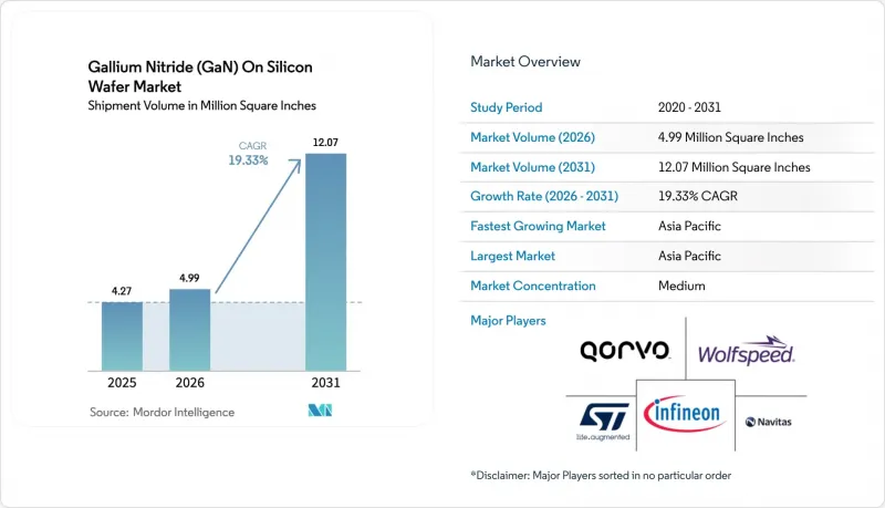
預計矽基基板的氮化鎵(GaN)晶片(GaN-on-Si晶片)的市場規模將從2025年的427萬平方英寸擴大到2026年的499萬平方英寸,到2031年達到1207萬平方英寸,2026年至20319年的複合年成長率為19.3%。
從傳統矽晶片到寬能隙設計的穩定轉變,使得更高的開關頻率、更佳的熱導率以及超過每立方英吋3千瓦的功率密度成為可能。原始設備製造商(OEM)正在加速推進200毫米GaN-on-Si晶片的認證,以滿足800V電動汽車牽引逆變器、強制性USB-C PD 3.1快速充電標準以及基於衛星的5G非地面網路部署的需求。隨著整合設備製造商、代工廠和無晶圓廠新創公司獲得快速充電適配器、資料中心電源和雷射雷達驅動器的設計訂單,競爭壓力日益加劇。同時,北美和歐洲的政府補貼正在加速300毫米試點生產線的建設,縮短商業化進程。
全球矽基基板氮化鎵 (GaN) 晶片的市場趨勢與見解。
一條日益成熟的 200 毫米氮化鎵矽基生產線
2025年,多家裝置製造商獲得了200mm氮化鎵矽基晶圓的認證,因此能夠降低晶圓成本並擴大產量。英飛凌於2025年下半年開始提供客戶300mm氮化鎵功率元件樣品,目標在2026年底開始量產。 InnoScience計劃在2025年將其8吋生產線產能擴大到每月2萬片晶圓,並預計2030年將達到每月7萬片。 Navitas和PSMC於2025年第四季完成了200mm晶圓的認證,並計畫在2026年上半年提高產量。這些進展將縮短前置作業時間,支援雙源供應,並加速汽車、工業和消費性電子領域的應用。隨著規模經濟的改善,矽基基板的氮化鎵晶圓市場正受益於與超接面矽的成本相當。
由於MOCVD產能的提高,外延晶片成本降低。
設備供應商正在推出多晶圓行星式反應器,可將產能提升高達 60%,在兩年內將外延成本降低約三分之一。 Veeco 的 Propel 平台可運作處理八片 200 毫米晶圓,並利用原位測量功能確保精確的製程控制。 AIXTRON 的 G5+C 每次循環可處理 19 片晶圓,縮短循環時間並提高良率。成本的降低使得這些產品能夠應用於 USB-C 適配器和無線充電器等消費性電子產品中,而這些產品先前對組件成本非常敏感。無廠半導體公司現在能夠進入大規模生產設計市場,並將其在矽基氮化鎵 (GaN) 晶圓市場的佔有率擴展到入門級價格範圍。
螺紋位移會影響尺寸大於 8 英吋的螺紋的屈服強度。
在矽基板上進行異質外延生長會產生穿透位錯,從而降低擊穿電壓並增加漏電流。在 200 毫米晶圓上,位錯密度可達 1 × 10⁸ cm⁻² 至 5 × 10⁸ cm⁻²,導致初始批次的良率降低高達 20%。在 300 毫米晶圓上,更長的熱梯度會加劇邊緣應力和翹曲,從而延長認證測試所需的時間和資本投入。儘管裝置製造商正在引入梯度 AlGaN 緩衝層和原位氮化物中階,但學習曲線仍減緩了基板GaN(氮化鎵)晶圓市場的擴張速度。
細分市場分析
2025年,150mm規格的晶圓出貨量佔比達53.92%。這主要得益於成熟的外延製程和折舊免稅額的設備基礎所帶來的經濟效益。然而,預計到2031年,200mm規格的晶圓出貨量將以20.37%的複合年成長率成長,並且隨著良率曲線的成熟,晶圓成本預計將降低35%至45%。安森美半導體已透過與Innoscience和GlobalFoundries的合作,確保了200mm規格的雙源產能,並計劃於2026年上半年提供樣品。因此,矽基基板的氮化鎵(GaN)晶圓市場正逐漸向200mm規格轉變,100mm規格仍將主要應用於科研和小規模國防領域。
英飛凌於2025年10月宣布將開始向客戶提供300mm氮化鎵(GaN)樣品,凸顯了其積極的規模化策略,旨在進軍汽車和工業領域的量產市場。 imec的300mm中試生產線將把GaN與先進的CMOS製程整合,目標是單晶片電源管理IC。初期能否成功取決於能否有效降低晶圓翹曲和位錯。如果製程控制成功,300mm矽基基板GaN晶圓的市場規模優勢可望重現矽的成本成長曲線,並加速其商品化進程。
到2025年,矽基基板的氮化鎵(GaN)晶圓將佔總產量的57.49%,預計到2031年將以每年19.78%的速度成長,這得益於其與200毫米和300毫米矽晶圓廠的兼容性以及通用的前驅體供應。這種成本優勢支持了消費電子和汽車應用領域的大規模生產,鞏固了其在矽基基板氮化鎵(GaN)晶圓市場的主導地位。同時,碳化矽(SiC)基板上的氮化鎵(GaN)基板仍局限於軍事雷達和衛星轉發器等特定應用領域,在這些領域,其卓越的導熱性和性能足以彌補四倍的價格溢價。
藍寶石基板上的氮化鎵(GaN)在光電子產業中仍被廣泛應用,尤其是在微型發光二極體(micro-LED)和紫外發光裝置方面。雖然純GaN基板能夠達到最低的位錯密度,但其成本過高,難以在小規模批量科研級生產以外的實用化中發揮作用。因此,市場參與企業正將研發重點放在超晶格緩衝層技術的創新上,以提高矽基GaN的可靠性,並將電壓範圍擴展至1200V。這意味著矽在基板GaN(氮化鎵)晶圓市場中仍佔有穩固的地位。
《矽基基板氮化鎵(GaN)晶圓市場報告》以晶圓直徑(100毫米、150毫米、200毫米)、基板類型(矽基板上的GaN、碳化矽基板上的GaN等)、元件應用(電動電子、射頻電等)、終端機基底(汽車/防電)、航太/防電板和電力地區進行電碼和電力地區。市場預測以體積(平方英吋)為單位。
區域分析
預計到2025年,亞太地區將佔全球出貨量的62.53%,並在2031年之前以20.27%的複合年成長率成長。中國正在支持Innoscience公司五年內實現每月7萬片晶圓的產能目標,而台灣地區則在探索將GaN-CMOS技術應用於行動和汽車產品。日本正利用ROHM、東芝和三菱電機等公司數十年來在化合物半導體領域的專業技術,而韓國則將目標瞄準資料中心和5G功率模組。印度為試點生產線提供激勵措施,但商業化生產仍處於起步階段,因此,矽基基板的氮化鎵(GaN)晶圓市場仍以東亞生態系統為主導。
北美正受惠於《晶片與科學法案》提供的520億美元資金。 MACOM公司已為其GaN-on-SiC射頻產品線獲得初步支持,凸顯了聯邦政府對保障寬能隙半導體供應的承諾。美國晶圓代工廠正與無晶圓廠新創公司合作開發汽車級GaN元件,而加拿大則在推進其北極監視雷達專案。一家墨西哥組裝廠與一家電動車工廠位於同一廠址,進一步擴大了SiC基板GaN(氮化鎵)晶圓市場的在地化優勢。
在歐洲,歐盟晶片技術創新與應用法案(CHIPS Act)提供的430億歐元資金和IPCEI微電子技術津貼81億歐元正推動著相關領域的發展,這些資金正用於投資英飛凌的300毫米中試生產線和弗勞恩霍夫的寬能隙項目等項目。法國在超寬能隙材料領域主導IPCEI叢集,英國則專注於用於衛星通訊的射頻裝置。荷蘭的ASML公司正在開發用於氮化鎵圖形化的微影術設備,而義大利則在推廣義法半導體的MasterGaN平台。除這三大主要國家外,南美洲、中東和非洲仍處於發展初期,目前僅在巴西和阿拉伯聯合大公國有先導計畫與使用氮化鎵的可再生能源相關的試點計畫。
其他好處:
- Excel格式的市場預測(ME)表
- 3個月的分析師支持
目錄
第1章:引言
- 市場分析與定義的前提條件
- 分析範圍
第2章 分析方法
第3章執行摘要
第4章 市場狀況
- 市場概覽
- 產業價值鏈分析
- 技術展望
- 對影響市場的宏觀經濟因素進行評估
- 市場促進因素
- 一條日益成熟的 200 毫米氮化鎵矽基生產線
- 由於MOCVD產能的提高,外延晶片成本降低。
- 800V電動車動力傳動系統架構的激增
- 強制採用 USB-C PD3.1 240W 快速充電。
- 擴大NTN衛星5G回程傳輸的部署。
- 政府對寬能隙晶片製造的獎勵(晶片、歐盟IPCEI)
- 市場限制因素
- 螺紋位錯對尺寸大於 8 英吋的屈服強度的影響
- 8吋氮化鎵生長設備供不應求
- IDM 和代工廠之間 IP 許可的障礙
- 200mm級晶圓因熱不配而產生的翹曲
- 波特五力分析
- 新參與企業的威脅
- 供應商議價能力
- 買方的議價能力
- 替代品的威脅
- 競爭公司之間的競爭關係
第5章:預測市場規模與成長率
- 依晶圓直徑
- 100 毫米(4 吋)
- 150 毫米(6 吋)
- 200 毫米(8 吋)
- 依基板類型
- 矽基基板的氮化鎵(GaN-on-Silicon)
- 碳化矽基板上的氮化鎵(GaN-on-Silicon 基板)
- 藍寶石基板上的氮化鎵(GaN-on-Sapphire)
- 原生GaN(體)
- 裝置應用程式
- 電力電子
- 射頻(RF)設備
- 光電子學(LED和雷射)
- 其他用途
- 按最終用途行業分類
- 汽車和電動車
- 航太/國防
- 可再生能源和儲能
- 家用電子電器
- 溝通
- 工業電力系統
- 按地區
- 北美洲
- 美國
- 加拿大
- 墨西哥
- 歐洲
- 德國
- 英國
- 法國
- 其他歐洲國家
- 亞太地區
- 中國
- 日本
- 印度
- 韓國
- 台灣
- 亞太其他地區
- 南美洲
- 中東
- 非洲
- 北美洲
第6章 競爭情勢
- 市場集中度
- 策略趨勢
- 市佔率分析
- 公司簡介
- Wolfspeed Inc.
- Qorvo Inc.
- NXP Semiconductors NV
- Infineon Technologies AG
- STMicroelectronics NV
- Renesas Electronics Corporation
- Efficient Power Conversion(EPC)Corp.
- Transphorm Inc.
- Toshiba Electronic Devices and Storage Corp.
- ROHM Co., Ltd.
- Navitas Semiconductor Corp.
- Innoscience(Suzhou)Technology Co., Ltd.
- MACOM Technology Solutions Holdings Inc.
- ON Semiconductor Corp.
- GaN Systems Inc.
- Power Integrations Inc.
- Skyworks Solutions Inc.
- Mitsubishi Electric Corp.
- Sumitomo Electric Industries Ltd.
- Integra Technologies Inc.
第7章 市場機會與未來展望
The Gallium Nitride (GaN) on Silicon Wafer market size is expected to increase from 4.27 million square inches in 2025 to 4.99 million square inches in 2026 and reach 12.07 million square inches by 2031, growing at a CAGR of 19.33% over 2026-2031.
Robust migration from legacy silicon toward wide-bandgap designs is enabling higher switching frequencies, elevated thermal conductivity, and power densities above 3 kW per cubic inch. Original equipment manufacturers are fast-tracking 200 mm GaN-on-Si qualification in response to 800-volt electric-vehicle traction inverters, mandated USB-C Power Delivery 3.1 fast-charging rules, and satellite-based 5G non-terrestrial network rollouts. Competitive pressure is intensifying as integrated device manufacturers, foundries, and fabless start-ups secure design wins in fast-charging adapters, data-center power supplies, and lidar drivers, while government subsidies in North America and Europe accelerate 300 mm pilot lines and compress commercialization timelines.
Global Gallium Nitride (GaN) On Silicon Wafer Market Trends and Insights
Maturing 200 mm GaN-on-Si Fabrication Lines
Multiple device makers qualified 200 mm GaN-on-Si wafers during 2025, cutting die costs and enabling higher unit volumes. Infineon began customer sampling of 300 mm GaN power devices in late 2025 and targets production by end-2026. Innoscience plans to scale to 20,000 wafers per month on 8-inch lines by 2025 and reach 70,000 by 2030. Navitas and PSMC completed 200 mm qualification in fourth-quarter 2025 and will ramp production in first-half 2026. These moves shorten lead times, support dual-sourcing, and spur adoption in automotive, industrial, and consumer segments. The Gallium Nitride (GaN) on Silicon Wafer market benefits from cost parity with super-junction silicon as scale economies improve.
Falling Epi-Wafer Costs Due to Higher MOCVD Throughput
Tool vendors have released multi-wafer planetary reactors that raise throughput by up to 60%, lowering epitaxial costs by roughly one-third within two years. Veeco's Propel platform processes eight 200 mm wafers per run with in-situ metrology for tighter process control. AIXTRON's G5+C handles 19 wafers per cycle, reducing cycle time and boosting yield. Lower costs open consumer applications such as USB-C adapters and wireless chargers that were previously bill-of-materials sensitive. Fabless firms can now bid for high-volume designs, expanding the Gallium Nitride (GaN) on Silicon Wafer market footprint across entry-level price points.
Threading Dislocations Impacting Yield Beyond 8 inch
Heteroepitaxial growth on silicon introduces threading dislocations, which degrade the breakdown voltage and increase leakage. Dislocation densities of 1X108 cm-2 to 5X108 cm-2 persist at 200 mm, trimming yields by up to 20% in early lots. Longer thermal gradients at 300 mm worsen edge stress and bow, extending qualification and capex. Device makers are adding graded AlGaN buffers and in-situ nitride interlayers, yet the learning curve slows the Gallium Nitride (GaN) on Silicon Wafer market ramp.
Other drivers and restraints analyzed in the detailed report include:
- Surge in 800 V Electric-Vehicle Powertrain Architectures
- Mandatory USB-C PD 3.1 240 W Fast-Charging Adoption
- Limited Availability of 8 inch GaN Growth Tools
For complete list of drivers and restraints, kindly check the Table Of Contents.
Segment Analysis
The 150 mm format accounted for 53.92% of shipments in 2025 as mature epitaxial recipes and depreciated tool bases supported attractive economics. However, the 200 mm tier is projected to register a 20.37% CAGR through 2031, providing 35-45% die cost savings once yield curves mature. onsemi secured dual-source 200 mm capacity through partnerships with Innoscience and GlobalFoundries, with samples due in first-half of 2026. The Gallium Nitride (GaN) on Silicon Wafer market therefore pivots toward 200 mm as mainstream, while 100 mm remains limited to research and low-volume defense needs.
Infineon's customer sampling of 300 mm GaN in October 2025 underscores an aggressive scaling roadmap aimed at automotive and industrial volumes. imec's 300 mm pilot line integrates GaN with advanced CMOS to target single-chip power-management ICs. Early success will depend on mitigating wafer bow and threading dislocations. If process control succeeds, Gallium Nitride (GaN) on Silicon Wafer market size advantages at 300 mm could replicate historical silicon cost curves and accelerate commoditization.
GaN-on-silicon held 57.49% of 2025 volume and is forecast to grow at 19.78% through 2031, anchored by compatibility with 200 mm and 300 mm silicon fabs and shared precursor supply chains. This cost leadership underpins high-volume consumer and automotive applications, reinforcing dominance within the Gallium Nitride (GaN) on Silicon Wafer market. GaN-on-silicon carbide, despite superior thermal conductivity, remains niche for military radar and satellite transponders where performance trumps a four-fold price premium.
GaN-on-sapphire continues to serve the optoelectronics industry, especially micro-LEDs and ultraviolet emitters. Native GaN substrates deliver the lowest dislocation densities but are cost-prohibitive beyond small research lots. Consequently, market participants allocate R&D to superlattice buffer innovations that raise GaN-on-silicon reliability and extend its addressable voltage up to 1,200 V, keeping the Gallium Nitride (GaN) on Silicon Wafer market share firmly in silicon's corner.
The Gallium Nitride (GaN) On Silicon Wafer Market Report is Segmented by Wafer Diameter (100 Mm, 150 Mm, and 200 Mm), Substrate Type (GaN-On-Silicon, GaN-On-Silicon Carbide, and More), Device Application (Power Electronics, Radio-Frequency Devices, and More), End-Use Industry (Automotive and EV, Aerospace and Defense, and More), and Geography. The Market Forecasts are Provided in Terms of Volume (Square Inches).
Geography Analysis
Asia-Pacific accounted for 62.53% of 2025 volume and is slated to grow at a 20.27% CAGR through 2031. China backs Innoscience's plan to reach 70,000 wafers per month over five years, while Taiwan explores GaN-CMOS integration for mobile and automotive products. Japan leverages decades of compound semiconductor expertise at ROHM, Toshiba, and Mitsubishi Electric, whereas South Korea targets data center and 5G power modules. India offers incentives for pilot lines, but commercial output remains embryonic, so the Gallium Nitride (GaN) on Silicon Wafer market continues to center on East-Asian ecosystems.
North America benefits from USD 52 billion in CHIPS and Science Act funding. MACOM secured preliminary support for a GaN-on-SiC RF line, highlighting the federal commitment to the security of wide-bandgap supply. U.S. foundries collaborate with fabless start-ups to build automotive-grade GaN devices, while Canada advances Arctic surveillance radar programs. Mexican assembly sites co-locate with electric-vehicle plants, extending regionalization advantages within the Gallium Nitride (GaN) on Silicon Wafer market.
Europe advances through EUR 43 billion in EU CHIPS Act resources and EUR 8.1 billion in IPCEI microelectronics grants, funneling capital to Infineon's 300 mm pilot line and Fraunhofer wide-bandgap projects. France heads an IPCEI cluster on ultra-wide-bandgap materials, and the United Kingdom focuses on RF devices for satellite links. ASML in the Netherlands explores lithography tooling for GaN patterning, while Italy promotes STMicroelectronics' MasterGaN platform. Outside the core triad, South America, the Middle East, and Africa remain nascent, with isolated renewable-energy pilots using GaN in Brazil and the United Arab Emirates.
- Wolfspeed Inc.
- Qorvo Inc.
- NXP Semiconductors N.V.
- Infineon Technologies AG
- STMicroelectronics N.V.
- Renesas Electronics Corporation
- Efficient Power Conversion (EPC) Corp.
- Transphorm Inc.
- Toshiba Electronic Devices and Storage Corp.
- ROHM Co., Ltd.
- Navitas Semiconductor Corp.
- Innoscience (Suzhou) Technology Co., Ltd.
- MACOM Technology Solutions Holdings Inc.
- ON Semiconductor Corp.
- GaN Systems Inc.
- Power Integrations Inc.
- Skyworks Solutions Inc.
- Mitsubishi Electric Corp.
- Sumitomo Electric Industries Ltd.
- Integra Technologies Inc.
Additional Benefits:
- The market estimate (ME) sheet in Excel format
- 3 months of analyst support
TABLE OF CONTENTS
1 INTRODUCTION
- 1.1 Study Assumptions and Market Definition
- 1.2 Scope of the Study
2 RESEARCH METHODOLOGY
3 EXECUTIVE SUMMARY
4 MARKET LANDSCAPE
- 4.1 Market Overview
- 4.2 Industry Value-Chain Analysis
- 4.3 Technological Outlook
- 4.4 Impact of Macroeconomic Factors on the Market
- 4.5 Market Drivers
- 4.5.1 Maturing 200 Mm GaN-on-Si Fabrication Lines
- 4.5.2 Falling Epi-Wafer Costs Due To Higher MOCVD Throughput
- 4.5.3 Surge In 800 V EV Powertrain Architectures
- 4.5.4 Mandatory USB-C PD3.1 240 W Fast-Charging Adoption
- 4.5.5 Rising Deployment Of Satellite-Based 5G NTN Backhaul
- 4.5.6 Government Incentives For Wide-Bandgap Fabs (CHIPS, EU IPCEI)
- 4.6 Market Restraints
- 4.6.1 Threading Dislocations Impacting Yield Beyond 8 Inch
- 4.6.2 Limited Availability Of 8 Inch GaN Growth Tools
- 4.6.3 IP Cross-Licensing Barriers Among IDMs and Foundries
- 4.6.4 Thermal Mismatch Induced Wafer Bow At ?200 mm
- 4.7 Porter's Five Forces Analysis
- 4.7.1 Threat of New Entrants
- 4.7.2 Bargaining Power of Suppliers
- 4.7.3 Bargaining Power of Buyers
- 4.7.4 Threat of Substitutes
- 4.7.5 Competitive Rivalry
5 MARKET SIZE AND GROWTH FORECASTS (VOLUME)
- 5.1 By Wafer Diameter
- 5.1.1 100 mm (4 inch)
- 5.1.2 150 mm (6 inch)
- 5.1.3 200 mm (8 inch)
- 5.2 By Substrate Type
- 5.2.1 GaN-on-Silicon
- 5.2.2 GaN-on-Silicon Carbide
- 5.2.3 GaN-on-Sapphire
- 5.2.4 Native GaN (Bulk)
- 5.3 By Device Application
- 5.3.1 Power Electronics
- 5.3.2 Radio-Frequency Devices
- 5.3.3 Optoelectronics (LED and Laser)
- 5.3.4 Other Applications
- 5.4 By End-Use Industry
- 5.4.1 Automotive and EV
- 5.4.2 Aerospace and Defense
- 5.4.3 Renewable Energy and Storage
- 5.4.4 Consumer Electronics
- 5.4.5 Telecommunications
- 5.4.6 Industrial Power Systems
- 5.5 By Geography
- 5.5.1 North America
- 5.5.1.1 United States
- 5.5.1.2 Canada
- 5.5.1.3 Mexico
- 5.5.2 Europe
- 5.5.2.1 Germany
- 5.5.2.2 United Kingdom
- 5.5.2.3 France
- 5.5.2.4 Rest of Europe
- 5.5.3 Asia-Pacific
- 5.5.3.1 China
- 5.5.3.2 Japan
- 5.5.3.3 India
- 5.5.3.4 South Korea
- 5.5.3.5 Taiwan
- 5.5.3.6 Rest of Asia-Pacific
- 5.5.4 South America
- 5.5.5 Middle East
- 5.5.6 Africa
- 5.5.1 North America
6 COMPETITIVE LANDSCAPE
- 6.1 Market Concentration
- 6.2 Strategic Moves
- 6.3 Market Share Analysis
- 6.4 Company Profiles (includes Global Level Overview, Market Level Overview, Core Segments, Financials as available, Strategic Information, Market Rank/Share, Products and Services, Recent Developments)
- 6.4.1 Wolfspeed Inc.
- 6.4.2 Qorvo Inc.
- 6.4.3 NXP Semiconductors N.V.
- 6.4.4 Infineon Technologies AG
- 6.4.5 STMicroelectronics N.V.
- 6.4.6 Renesas Electronics Corporation
- 6.4.7 Efficient Power Conversion (EPC) Corp.
- 6.4.8 Transphorm Inc.
- 6.4.9 Toshiba Electronic Devices and Storage Corp.
- 6.4.10 ROHM Co., Ltd.
- 6.4.11 Navitas Semiconductor Corp.
- 6.4.12 Innoscience (Suzhou) Technology Co., Ltd.
- 6.4.13 MACOM Technology Solutions Holdings Inc.
- 6.4.14 ON Semiconductor Corp.
- 6.4.15 GaN Systems Inc.
- 6.4.16 Power Integrations Inc.
- 6.4.17 Skyworks Solutions Inc.
- 6.4.18 Mitsubishi Electric Corp.
- 6.4.19 Sumitomo Electric Industries Ltd.
- 6.4.20 Integra Technologies Inc.
7 MARKET OPPORTUNITIES AND FUTURE OUTLOOK
- 7.1 White-Space and Unmet-Need Assessment
 中國LED外延片:市佔率分析、產業趨勢與統計及成長預測(2026-2031年)亞太地區LED外延片:市佔率分析、產業趨勢與統計及成長預測(2026-2031年)
 氮化鎵裝置市場預測至2034年-按產品類型、元件、電壓範圍、最終用戶和地區分類的全球分析氮化鎵基LED外延片:市佔率分析、產業趨勢與統計及成長預測(2026-2031年)氮化鎵矽基(GaN-on-Si)LED外延片:市佔率分析、產業趨勢與統計數據以及成長預測(2026-2031年)
 2026-2034年全球氮化鎵工業裝置市場規模、佔有率、趨勢與成長分析報告
 氮化鎵半導體裝置市場:2026-2032年全球市場預測(按裝置類型、晶圓尺寸、應用和最終用途產業分類)氮化鎵雷達系統市場:按類型、組件、頻寬、組件範圍和應用分類-2026年至2032年全球預測
 氮化鎵半導體市場:依產品、組件、晶圓尺寸、最終用途、國家及地區分類-全球產業分析、市場規模、市場佔有率及2025年至2032年預測
 高頻氮化鎵半導體市場分析及預測(至2035年):依類型、產品類型、服務、技術、應用、材料類型、裝置、部署類型、最終用戶和功能分類