


 |
市場調查報告書
商品編碼
2044056
氮化鎵矽基(GaN-on-Si)LED外延片:市佔率分析、產業趨勢與統計數據以及成長預測(2026-2031年)GaN-on-Silicon (GaN-on-Si) LED Epitaxial Wafer - Market Share Analysis, Industry Trends & Statistics, Growth Forecasts (2026 - 2031) |
||||||
※ 本網頁內容可能與最新版本有所差異。詳細情況請與我們聯繫。
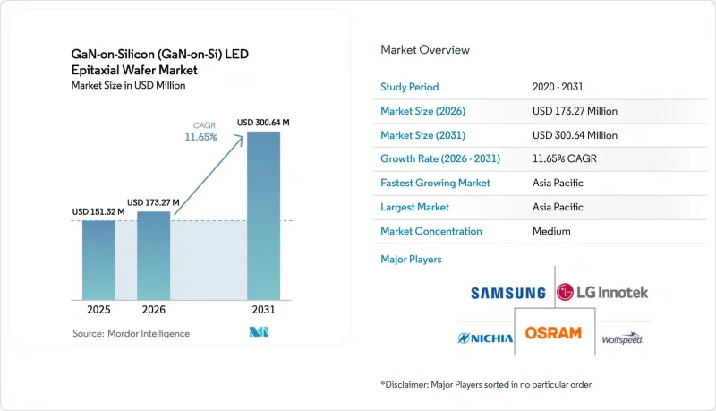
預計 GaN-on-Si LED 外延晶片的市場規模將從 2025 年的 1.51 億美元成長到 2026 年的 1.73 億美元,到 2031 年達到 3.01 億美元,2026 年至 2031 年的複合年成長率預計為 11.65%。
由於燈具光通量效率持續受到監管壓力、向200毫米製程轉型以及微型LED在擴增實境(AR)設備中的應用,GaN-on-Si外延技術的商業性吸引力日益增強。在照明產業,由於LED的普及,白熾燈和鹵素燈在經濟上已經過時,但美國、歐盟、中國和印度等地更嚴格的標準正在擴大更有效率晶片架構的潛在市場。代工廠將矽基基板與現有CMOS生產線的兼容性視為降低資本成本的途徑,促使供應商加速試用300毫米MOCVD設備,其晶粒生產能力是100毫米藍寶石生產線的九倍。垂直整合的顯示器專案(目標像素尺寸小於10微米)進一步強化了這一趨勢。在這一領域,GaN-on-Si技術省去了藍寶石製程中所需的晶圓-驅動器鍵合製程。由於大約有 15 家企業主導反應器生產能力,並擁有將缺陷密度控制在可接受範圍內的製程技術,因此競爭程度仍然相對較低。
全球氮化鎵矽基(GaN-on-Si)LED外延晶片市場趨勢及洞察
高效固體照明的需求日益成長
到2025年,固體照明將佔已安裝照明設備的65%,但國際能源總署(IEA)估計,到2026年,其效率還有提升30%的技術可能,這為氮化鎵矽基(GaN-on-Si)LED外延晶片市場留下了巨大的成長空間。美國能源局將於2028年7月生效的法規規定,燈具效率必須達到白熾燈或鹵素燈技術無法企及的水平,並明確將矽基替代基板方案列為可行的設計方案。面向住宅和商業維修的照明製造商目前面臨雙重壓力:既要降低組件成本,又要達到130 lm/W的效率基準值。與100毫米藍寶石晶片相比,使用大直徑矽晶片可將每流明成本降低高達25%。北美公用事業公司的補貼計劃,將獎勵與高效產品的上市掛鉤,正在推動市場需求的成長。這些因素綜合起來,將確保未來幾年整體生產的照明產品對矽上氮化鎵外延的需求將持續存在。
GaN-on-Si基板和藍寶石基板的潛在成本降低
矽晶圓的售價為每片200毫米50至70美元,約為同等尺寸藍寶石晶圓價格的八分之一。這帶來了結構上的優勢,隨著晶圓直徑的增加,這種差異會進一步擴大。 2025年的一項演示表明,5.25 × 10⁸ cm⁻²的位錯密度已成為標準,這縮小了與藍寶石的效率差距,同時保持了基板成本70%的差異。從製造成本的角度來看,據上海一家材料供應商稱,單條200毫米GaN-on-Si製程可以生產出單條100毫米藍寶石基板四倍的晶片面積,一台設備每年可供應50萬個用於汽車充電器的LED。然而,如此規模的盈利取決於維持85%以上的良率,而這一目標只有透過即時翹曲控制和最佳化緩衝層才能實現。隨著這些製程改進廣泛應用,矽的價格優勢有望抵消對成本敏感的終端市場中任何剩餘的效率下降。
GaN-on-Si外延生長中高位錯密度與良率挑戰
矽和氮化鎵之間17%的晶格失配導致位錯密度接近1 × 10⁹ cm⁻²。這比藍寶石基材料高出約兩個數量級,也是外量子效率下降10-15%的主要原因。雖然諸如60對AlN/GaN多層膜之類的緩衝技術可以抑制應力,但會增加反應時間,每片晶圓的成本高達12美元。在200毫米基板上,超過100微米的翹曲會使光刻和切割變得複雜,迫使一些晶圓廠放棄邊緣晶片,從而削弱大尺寸晶圓的成本優勢。目前進展不一。一些供應商報告的翹曲測量值小於30微米,但由於缺乏成熟的標準化工藝,平均良率低於藍寶石同類產品90%的基準水平。
細分市場分析
200mm規格填補了傳統150mm規格和新興300mm規格之間的空白,其成長速度超過了整體GaN-on-Si LED外延晶圓市場。即使到了2025年,150mm規格仍將佔據主導地位,出貨量佔比高達48.19%,這主要得益於其在中功率照明和背光領域的強勢地位。但目前的設備發展藍圖已明顯優先考慮更大直徑的規格。 2026年300mm反應器的產量預測凸顯了向12吋設備的策略性轉變,其晶片產量是100mm藍寶石晶片的九倍,這項計算結果引起了顯示面板製造商的強烈共鳴。 GaN-on-Si LED外延晶圓的市場規模優勢將隨著晶圓面積的增加而擴大,但這只有在最大限度減少邊緣去除和裂紋相關廢料的情況下才能實現。聲稱在 8 英寸晶圓上實現小於 30µm 翹曲的供應商報告稱,良率超過 90%,這表明製程控制,而不是簡單的直徑,才是決定經濟可行性的因素。
資本投資的分配也遵循類似的邏輯。已完成200毫米CMOS生產線折舊免稅額的代工廠,可以以新建藍寶石工廠成本的約60%將其腔室改造為GaN-on-Si生產線。這一數字對那些擔憂LED利潤率週期性波動的投資者來說極具吸引力。雖然100毫米和150毫米晶圓仍將繼續用於紫外線和原型製作應用,但分析人員預計,200毫米以上晶圓的新增產能將主要集中在200毫米及以上尺寸。向300毫米晶圓的過渡仍然面臨一些技術挑戰,尤其是在氣體流動均勻性和溫度梯度方面,但其優勢,尤其是在高解析度顯示領域,極具吸引力,多家領先的設備製造商已承諾在2027年前交付量產系統。
區域分析
亞太地區是矽基氮化鎵(GaN-on-Si)LED外延片市場製造與創新的驅動力。預計到2025年,該地區將佔全球銷售額的66.93%,其中中國大陸、台灣和韓國的國家級項目將推動該地區到2031年實現12.64%的複合年成長率。光是中國大陸就已投入800億元人民幣(約112億美元)用於微型LED基礎設施建設,其中大部分將用於建設200毫米和300毫米的GaN-on-Si晶圓廠,從而確保大直徑基板的在地採購。台灣和日本的供應商憑藉其材料科學專長和設備創新,進一步擴大了這一規模。日亞化學工業株式會社的無汞紫外線光刻舉措以及羅姆公司決定將其GaN製程內部化,都凸顯了供應鏈向內部化轉型的趨勢。
北美地區專注於高價值應用和政策主導的推廣。美國能源部一項將於2028年7月生效的決定將幾乎可以確保現有白熾燈泡庫存的淘汰,而安森美半導體等公司和全球晶圓代工廠也對將氮化鎵外延技術整合到現有CMOS生產線中表現出濃厚的興趣。歐洲市場正由德國英飛凌引領,該公司計劃在2025年第四季實現300毫米晶圓的出貨量,並將該地區打造成為汽車和工業功率裝置的中心。同時,南美洲、中東和非洲目前僅佔全球出貨量的個位數百分比,但由於離網太陽能照明計畫和工業現代化努力,預計到2020年代末,對低成本氮化鎵矽基LED的需求將進一步成長。
亞太地區的領先地位因垂直整合而進一步鞏固。中國大陸和台灣地區的企業擴大自主完成從氮化鎵原料生長到成品LED模組的各個環節,從而縮短供應鏈並加快產品上市速度。政府補貼降低了試生產線的風險,使得企業能夠嘗試300毫米規格的產品,而西方競爭對手則認為這種規格需要大量資金投入。然而,智慧財產權保護的挑戰和出口管制的不確定性為該地區的長期前景蒙上了一層陰影,促使跨國OEM廠商採取雙源策略,將北美和歐洲的外延生產能力納入其中。
其他好處:
- Excel格式的市場預測(ME)表
- 3個月的分析師支持
目錄
第1章:引言
- 研究假設和市場定義
- 調查範圍
第2章:調查方法
第3章執行摘要
第4章 市場狀況
- 市場概覽
- 市場促進因素
- 節能固體照明的需求日益成長
- GaN-on-Si基板和藍寶石基板的潛在成本降低
- 政府關於逐步淘汰白熾燈和鹵素燈泡的規定
- 擴大汽車LED在頭燈和ADAS感測器中的應用。
- 用於AR顯示器的GaN基微型LED陣列的整合
- 擴建200毫米和300毫米CMOS晶圓廠,用於GaN-on-Si外延生長
- 市場限制因素
- GaN-on-Si外延生長中高位錯密度與良率挑戰
- 來自藍寶石基LED晶圓的競爭
- 具有應力控制功能的圖案形成矽基基板供不應求
- 氮化鎵外延製程中智慧財產權訴訟的風險
- 產業分析
- 宏觀經濟因素對市場的影響
- 波特五力分析
- 供應商的議價能力
- 買方的議價能力
- 新進入者的威脅
- 替代品的威脅
- 競爭公司之間的競爭
第5章 市場規模與成長預測
- 依晶圓直徑
- 100毫米或更小
- 150 mm
- 200 mm
- 300毫米或以上
- 透過使用
- 一般照明
- 汽車照明
- 顯示器和背光
- 特殊和工業照明
- 按地區
- 北美洲
- 歐洲
- 亞太地區
- 世界其他地區
第6章 競爭情勢
- 市場集中度
- 策略趨勢
- 市佔率分析
- 公司簡介
- Nichia Corporation
- Wolfspeed Inc.
- Epistar Corporation
- OSRAM GmbH
- LG Innotek Co. Ltd.
- Samsung Electronics Co. Ltd.
- Plessey Semiconductors Ltd.
- Qorvo Inc.
- Infineon Technologies AG
- NXP Semiconductors NV
- Power Integrations Inc.
- Efficient Power Conversion Corporation
- Exagan SA
- STMicroelectronics NV
- Panasonic Corporation
- Toshiba Corporation
- ROHM Co. Ltd.
- Sumitomo Electric Industries Ltd.
- Sanan Optoelectronics Co. Ltd.
- Aixtron SE
- IQE plc
第7章 市場機會與未來展望
The GaN-on-Silicon LED epitaxial wafer market size is expected to increase from USD 0.151 billion in 2025 to USD 0.173 billion in 2026 and reach USD 0.301 billion by 2031, growing at a CAGR of 11.65% over 2026-2031.
Persistent regulatory pressure on lamp efficacy, the migration to 200 mm processing, and micro-LED adoption in augmented-reality (AR) devices are converging to widen the commercial appeal of GaN-on-Si epitaxy. Across lighting classes, LED penetration has already made incandescent and halogen formats economically obsolete, yet tightening standards in the United States, the European Union, China, and India are expanding the addressable market for more efficient die architectures. Foundries view the compatibility of silicon substrates with existing CMOS lines as a capital-saving lever, spurring vendors to pilot 300 mm MOCVD tools that can deliver nine times the die output of 100 mm sapphire runs. Momentum is reinforced by vertically integrated display programs targeting sub-10 µm pixels, where GaN-on-Si eliminates the wafer-to-driver bonding step that sapphire requires. Competitive dynamics remain moderate because roughly fifteen players control reactor capacity and hold the process know-how needed to keep defect densities within acceptable limits.
Global GaN-on-Silicon (GaN-on-Si) LED Epitaxial Wafer Market Trends and Insights
Increasing Demand for Energy-Efficient Solid-State Lighting
Solid-state lighting accounted for 65% of installed luminaires in 2025, yet the International Energy Agency calculated in 2026 that another 30% efficiency gain remains technically achievable, leaving ample headroom for the GaN-on-Silicon LED epitaxial wafer market to grow. The U.S. Department of Energy rule, effective July 2028, mandates lamp efficacies that cannot be met by incandescent or halogen technology, explicitly citing alternative substrate options, including silicon, as viable design pathways. Fixture makers addressing residential and commercial retrofits now face dual pressures to lower bill-of-materials cost and exceed 130 lm/W efficacy thresholds, and larger-diameter silicon wafers reduce per-lumen cost by up to 25% compared with 100 mm sapphire. Utility rebate programs in North America reinforce demand by linking incentives to high-efficacy product listings. Collectively, these forces sustain a multiyear pull for GaN-on-Si epitaxy across high-volume lighting classes.
Cost Reduction Potential of GaN-on-Si Substrates Versus Sapphire
Silicon substrates sell for USD 50-70 per 200 mm wafer, roughly one-eighth the price of comparable sapphire, creating a structural advantage that expands as diameters scale upward. Demonstrations in 2025 showed that 5.25 X 108 cm-2 dislocation densities are now routine, cutting the efficiency gap with sapphire while still preserving a 70% substrate-cost delta. In reactor economics, a 200 mm GaN-on-Si run produces four times the die area of a 100 mm sapphire load, enabling a single tool to support 500,000 onboard-charger LEDs yearly, according to a Shanghai materials supplier. Such scale profitability, however, hinges on maintaining yields above 85%, a target achievable only with real-time warp control and optimized buffer stacks. As these process refinements diffuse, silicon's price advantage is expected to offset residual efficiency penalties in cost-sensitive end markets.
High Dislocation Density and Yield Challenges in GaN-on-Si Epitaxy
The 17% lattice mismatch between silicon and gallium nitride drives threading dislocation densities near 1 X 109 cm-2, roughly two orders of magnitude higher than sapphire-based material and a primary cause of 10-15% lower external quantum efficiency. Buffer techniques such as 60-pair AlN/GaN multilayers can suppress stress but add up to USD 12 per wafer in extra reactor time. Warp above 100 µm on 200 mm substrates complicates lithography and dicing, forcing some fabs to scrap edge die, which undermines the cost benefits of larger wafers. Progress is uneven: while a handful of suppliers now report sub-30 µm bow metrics, the lack of standardized processes keeps average yields below the 90% benchmark enjoyed by sapphire competitors.
Other drivers and restraints analyzed in the detailed report include:
- Expansion of 200 mm and 300 mm CMOS Fabs for GaN-on-Si Epi
- Growth of Automotive LED Adoption for Headlamps and ADAS Sensors
- Competition from Sapphire-Based LED Wafers
For complete list of drivers and restraints, kindly check the Table Of Contents.
Segment Analysis
The 200 mm tier, representing the bridge between legacy 150 mm and emerging 300 mm production, is expanding faster than the overall GaN-on-Silicon LED epitaxial wafer market. In 2025 the 150 mm format still dominated shipments at 48.19%, thanks to its entrenched position in mid-power illumination and backlighting, yet equipment roadmaps now overwhelmingly favor larger diameters. Volume evaluations of 300 mm reactors in 2026 underscore a strategic pivot to 12-inch tools that yield ninefold more die than 100 mm sapphire lots, an arithmetic that resonates strongly with display panel makers. The GaN-on-Silicon LED epitaxial wafer market size advantage grows as wafer area increases, but only if edge exclusion and crack-related scrap remain minimal. Suppliers claiming sub-30 µm bow on 8-inch substrates report yields north of 90%, demonstrating that process control rather than raw diameter dictates economic viability.
Capital allocation is following the same logic. Foundries with depreciated 200 mm CMOS lines can retrofit chambers for GaN-on-Si at roughly 60% of the cost of new sapphire fabs, a figure that appeals to investors wary of cyclical LED margins. Although 100 mm and 150 mm wafers will persist in UV and prototyping roles, analysts expect new capacity additions after 2027 to skew heavily toward 200 mm and above. The inflection to 300 mm still confronts technical hurdles, most notably uniform gas flow and temperature gradients, but the payback, especially for high-pixel-count displays, is compelling enough that several tier-one equipment makers have committed to shipping production systems by 2027.
The GaN-On-Silicon (GaN-On-Si) LED Epitaxial Wafer Market Report is Segmented by Wafer Diameter (Up To 100 Mm, 150 Mm, 200 Mm, and 300 Mm and Above), Application (General Lighting, Automotive Lighting, Display and Backlighting, and Specialty and Industrial Lighting), and Geography. The Market Forecasts are Provided in Terms of Value (USD).
Geography Analysis
Asia-Pacific is both the manufacturing and innovation engine of the GaN-on-Silicon LED epitaxial wafer market. The region accounted for 66.93% of 2025 revenue, and national programs in China, Taiwan, and South Korea are forecast to drive a 12.64% CAGR through 2031. China alone has earmarked RMB 80 billion (USD 11.2 billion) for micro-LED infrastructure, much of which is dedicated to 200 mm and 300 mm GaN-on-Si fabs, ensuring local availability of large-diameter substrates. Taiwanese and Japanese vendors complement this scale with materials science expertise and equipment innovation. Nichia's mercury-free UV initiative and ROHM's decision to internalize GaN processes underscore a trend toward captive supply chains.
North America concentrates on high-value applications and policy-led adoption. The Department of Energy ruling that becomes enforceable in July 2028 virtually guarantees replacement of legacy incandescent stock, whereas partnerships such as onsemi-GlobalFoundries signal a willingness to incorporate GaN epitaxy into brownfield CMOS lines. European participation is anchored by Germany's Infineon, whose 300 mm wafer deliveries in Q4 2025 position the region as a node for automotive and industrial power devices. While South America, the Middle East, and Africa currently absorb only single-digit percentages of global shipments, off-grid solar lighting initiatives and industrial modernization efforts are likely to generate incremental demand for low-cost GaN-on-Si LEDs by the end of the decade.
Asia-Pacific's dominance is enhanced by vertical integration: Chinese and Taiwanese firms increasingly handle everything from raw GaN growth to finished LED modules, compressing the supply chain and accelerating time-to-market. Government subsidies lower risk for pilot lines, allowing experimentation with 300 mm formats that Western competitors regard as capital intensive. Nonetheless, intellectual-property enforcement challenges and export-control uncertainties temper the region's longer-term outlook, encouraging multinational OEMs to adopt dual-sourcing strategies that include North American or European epitaxial capacity.
- Nichia Corporation
- Wolfspeed Inc.
- Epistar Corporation
- OSRAM GmbH
- LG Innotek Co. Ltd.
- Samsung Electronics Co. Ltd.
- Plessey Semiconductors Ltd.
- Qorvo Inc.
- Infineon Technologies AG
- NXP Semiconductors N.V.
- Power Integrations Inc.
- Efficient Power Conversion Corporation
- Exagan SA
- STMicroelectronics N.V.
- Panasonic Corporation
- Toshiba Corporation
- ROHM Co. Ltd.
- Sumitomo Electric Industries Ltd.
- Sanan Optoelectronics Co. Ltd.
- Aixtron SE
- IQE plc
Additional Benefits:
- The market estimate (ME) sheet in Excel format
- 3 months of analyst support
TABLE OF CONTENTS
1 INTRODUCTION
- 1.1 Study Assumptions and Market Definition
- 1.2 Scope of the Study
2 RESEARCH METHODOLOGY
3 EXECUTIVE SUMMARY
4 MARKET LANDSCAPE
- 4.1 Market Overview
- 4.2 Market Drivers
- 4.2.1 Increasing Demand For Energy-Efficient Solid-State Lighting
- 4.2.2 Cost Reduction Potential Of GaN-on-Si Substrates Versus Sapphire
- 4.2.3 Government Regulations Phasing-Out Incandescent And Halogen Bulbs
- 4.2.4 Growth Of Automotive LED Adoption For Headlamps And ADAS Sensors
- 4.2.5 Integration Of GaN-Based Micro-LED Arrays For AR Displays
- 4.2.6 Expansion Of 200 mm And 300 mm CMOS Fabs For GaN-on-Si Epi
- 4.3 Market Restraints
- 4.3.1 High Dislocation Density And Yield Challenges In GaN-on-Si Epitaxy
- 4.3.2 Competition From Sapphire-Based LED Wafers
- 4.3.3 Limited Availability Of Patterned Si Substrates With Stress Control
- 4.3.4 Risk Of IP Litigation In GaN Epitaxy Processes
- 4.4 Industry Analysis
- 4.5 Impact Of Macroeconomic Factors On The Market
- 4.6 Porter's Five Forces Analysis
- 4.6.1 Bargaining Power Of Suppliers
- 4.6.2 Bargaining Power Of Buyers
- 4.6.3 Threat Of New Entrants
- 4.6.4 Threat Of Substitutes
- 4.6.5 Intensity Of Competitive Rivalry
5 MARKET SIZE AND GROWTH FORECASTS (VALUE)
- 5.1 By Wafer Diameter
- 5.1.1 Upto 100 mm
- 5.1.2 150 mm
- 5.1.3 200 mm
- 5.1.4 300 mm and Above
- 5.2 By Application
- 5.2.1 General Lighting
- 5.2.2 Automotive Lighting
- 5.2.3 Display and Backlighting
- 5.2.4 Specialty and Industrial Lighting
- 5.3 By Geography
- 5.3.1 North America
- 5.3.2 Europe
- 5.3.3 Asia-Pacific
- 5.3.4 Rest of the World
6 COMPETITIVE LANDSCAPE
- 6.1 Market Concentration
- 6.2 Strategic Moves
- 6.3 Market Share Analysis
- 6.4 Company Profiles (includes Global Level Overview, Market Level Overview, Core Segments, Financials as available, Strategic Information, Market Rank/Share, Products and Services, Recent Developments)
- 6.4.1 Nichia Corporation
- 6.4.2 Wolfspeed Inc.
- 6.4.3 Epistar Corporation
- 6.4.4 OSRAM GmbH
- 6.4.5 LG Innotek Co. Ltd.
- 6.4.6 Samsung Electronics Co. Ltd.
- 6.4.7 Plessey Semiconductors Ltd.
- 6.4.8 Qorvo Inc.
- 6.4.9 Infineon Technologies AG
- 6.4.10 NXP Semiconductors N.V.
- 6.4.11 Power Integrations Inc.
- 6.4.12 Efficient Power Conversion Corporation
- 6.4.13 Exagan SA
- 6.4.14 STMicroelectronics N.V.
- 6.4.15 Panasonic Corporation
- 6.4.16 Toshiba Corporation
- 6.4.17 ROHM Co. Ltd.
- 6.4.18 Sumitomo Electric Industries Ltd.
- 6.4.19 Sanan Optoelectronics Co. Ltd.
- 6.4.20 Aixtron SE
- 6.4.21 IQE plc
7 MARKET OPPORTUNITIES AND FUTURE OUTLOOK
- 7.1 White-Space and Unmet-Need Assessment
 中國LED外延片:市佔率分析、產業趨勢與統計及成長預測(2026-2031年)亞太地區LED外延片:市佔率分析、產業趨勢與統計及成長預測(2026-2031年)
 氮化鎵裝置市場預測至2034年-按產品類型、元件、電壓範圍、最終用戶和地區分類的全球分析氮化鎵基LED外延片:市佔率分析、產業趨勢與統計及成長預測(2026-2031年)
 2026-2034年全球氮化鎵工業裝置市場規模、佔有率、趨勢與成長分析報告
 氮化鎵半導體裝置市場:2026-2032年全球市場預測(按裝置類型、晶圓尺寸、應用和最終用途產業分類)矽基基板的氮化鎵(GaN)晶圓:市佔率分析、產業趨勢與統計、成長預測(2026-2031)氮化鎵雷達系統市場:按類型、組件、頻寬、組件範圍和應用分類-2026年至2032年全球預測
 氮化鎵半導體市場:依產品、組件、晶圓尺寸、最終用途、國家及地區分類-全球產業分析、市場規模、市場佔有率及2025年至2032年預測
 高頻氮化鎵半導體市場分析及預測(至2035年):依類型、產品類型、服務、技術、應用、材料類型、裝置、部署類型、最終用戶和功能分類