


 |
市場調查報告書
商品編碼
2044017
用於分立元件的矽晶圓:市場佔有率分析、行業趨勢和統計數據以及成長預測(2026-2031 年)Silicon Wafer For Discrete Devices - Market Share Analysis, Industry Trends & Statistics, Growth Forecasts (2026 - 2031) |
||||||
※ 本網頁內容可能與最新版本有所差異。詳細情況請與我們聯繫。
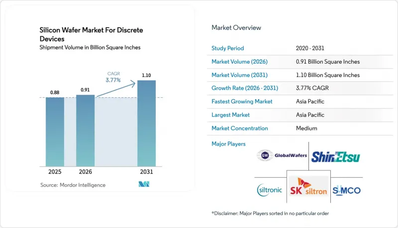
2025 年,分立元件用矽晶圓市場價值為 8.8 億平方英寸,預計到 2031 年將達到 11 億平方英寸,而 2026 年為 9.1 億平方英寸,預測期(2026-2031 年)複合年成長率為 3.77%。
隨著電池式電動車、可再生能源逆變器和工廠自動化驅動器對電流的要求高於傳統家用電子電器,市場對功率基板的需求正在轉向功率基板。美國《晶片與科學法案》、歐洲《晶片法案》以及中國第三期積體電路基金等政府補貼正在加速200毫米生產線的擴張,縮短設備投資回收期,並加劇供應商之間的競爭。預計2025年初,多晶矽現貨價格將回升至每公斤8-9美元,利潤率的波動促使晶圓供應商在長期合約中加入指數級遞增條款。目前,汽車電氣化正在推動基板的分配,電池式電動車平台中每輛車的獨立元件數量增加了兩倍多,超過1200個。此外,工業馬達驅動裝置的維修正成為推動產量成長的第二個支柱。同時,對中國先進薄膜沉積和微影術設備的出口限制造成了供應鏈的兩極化,導致中國以外買家的前置作業時間延長。因此,跨國OEM廠商正日益推廣晶圓的跨區域雙重採購。
分立元件用矽晶圓市場趨勢與展望
電動車快速充電基礎設施的擴建需要大電流二極體
功率為350千瓦的超快充電樁目前已成為中國、歐洲和美國高速公路沿線的主流配置,每個充電樁需要8到12個額定電壓為1200至1700伏特、電流為100安培或以上的獨立二極體。 2025年2月,Wolfspeed公司發表了一款用於這些整流器的200毫米SiC矽基外延平台,顯示隨著突波電流需求的增加,晶圓的翹曲、畸變和缺陷密度等指標需要更加嚴格。中國國家電網公司計劃在2025年新增12萬個超快速充電樁,這將對用於大電流二極體的基板產生約1500萬至2000萬平方英寸的額外需求。歐盟的《替代燃料基礎設施法規》要求在2027年前建立可互通的充電網路,這將鞏固大量使用獨立元件的組合充電系統(CCS)協議。由於高阻矽基板上碳化矽肖特基二極體的開關頻率超過 50 kHz,市場需求不斷成長,推動了該技術的日益普及。這一趨勢導致特種基板的出貨量增加,甚至超過了優質拋光襯底的出貨量。
GaN/SiC混合模組的採用增加了對高阻矽基基板的需求。
混合功率模組將GaN HEMT和SiC二極體共封裝在高阻矽基板上,與單晶片SiC相比,每瓦成本降低了30%至40%,使汽車製造商能夠實現每瓦0.15美元的系統目標。英飛凌於2024年3月發布的CoolSiC裝置採用了這種架構,目前已在200毫米晶圓上出貨,其電阻規格為1000至10000歐姆厘米。意法半導體報告稱,2024年混合模組銷量成長了28%,其中65%的銷量來自汽車製造商,凸顯了這些基板的商業性勢頭。日本經濟產業省累計450億日圓(約3.07億美元)用於支持國內高阻矽的生產,明確顯示國家政策與汽車電力電子產業緊密相關。用於 650V 裝置的矽基氮化鎵晶圓要求位錯密度低於 10^6 cm⁻²,且晶體取向為 111。然而,只有專業的晶圓供應商才能滿足這項要求,這為進入供應鏈設置了很高的門檻。
多晶矽價格波動與能源成本
2022年至2025年間,多晶矽價格在每公斤6美元至35美元之間波動。儘管現貨價格在2025年初回升至每公斤8-9美元,但長期合約價格仍維持在每公斤11-13美元,這給消費級晶圓的利潤率帶來了壓力。歐洲生產商面臨的電力成本是2019年的三倍,平均為每千瓦時0.18歐元(每千瓦時0.20美元),而晶體生長每公斤晶錠大約消耗225千瓦時的電力,進一步加劇了這一影響。在中國,每千瓦時0.35元人民幣(每千瓦時0.05美元)的低額工業補貼抵消了能源密集型生產成本,而美國的《通貨膨脹削減法案》則為使用清潔能源提供每千瓦時0.03美元的生產稅額扣抵。五家多晶矽供應商的供應集中加劇了價格波動,迫使晶圓供應商要麼在合約中加入價格轉嫁條款,要麼承擔價格大幅上漲期間毛利率為負的風險。
細分市場分析
截至2025年,200毫米晶圓將佔據矽晶圓市場59.66%的佔有率,這得益於已完全折舊的晶圓廠資產。這些資產在分立電晶體和二極體的生產方面持續保持著卓越的折舊免稅額效益。日本、捷克和馬來西亞的汽車級晶圓廠的產運轉率均超過90%。這是因為此尺寸的晶圓最佳化了產能和產品配置柔軟性之間的平衡。雖然300毫米基板目前僅佔矽晶圓市場規模的24%,但預計到2031年,隨著整合電源管理IC和多晶片模擬模組轉向更大尺寸的晶圓以將光刻開銷分散到數百個晶片上,其市場佔有率將以每年4.52%的速度成長。德克薩斯計畫將其位於理查森的工廠40%的產能用於類比和電源產品,以滿足對300毫米晶圓的需求。
在射頻二極體、閘流體和感測器等特定細分市場,由於特定的晶體取向需要更小的直徑,150毫米晶圓仍然存在。 SEMI預測,到2028年,所有半導體領域的200毫米晶圓出貨量將以每年1.2%的速度下降,但對分立元件的需求部分抵消了這一降幅,吸收了記憶體和MCU生產釋放的產能。此外,出於對供應鏈韌性的擔憂,汽車製造商正將其200毫米晶圓的採購來源多元化,轉向日本和中國,以此對沖地震和地緣政治風險等區域性風險。
《分立元件用矽晶圓市場報告》依晶圓直徑(150毫米及以下、200毫米、300毫米)、晶圓類型(拋光面、外延面、SOI、特種矽)、終端用戶(家用電子電器、工業、電信、汽車等)及地區(北美、歐洲、亞太等)進行細分。市場預測以體積(平方英吋)為單位。
區域分析
亞太地區預計在2025年將佔全球晶圓出貨量的81.84%,並預計在2031年之前以4.79%的複合年成長率成長,這主要得益於日本、台灣和中國不斷擴大其200毫米晶圓產能。信越化學和SUMCO在2024年總合出貨4.5億平方英吋。兩家公司均採用其專有的直拉法(柴可拉斯基法)來保持電阻率均勻性在±5%以內。台灣的GlobalWafers公司將其2024年產能的35%分配給了單一客戶,並透過與安森美半導體(ON Semiconductor)和維沙伊(Vishai)簽訂的長期契約,保持了85%以上的產運轉率。在省級政府80億元人民幣(約11億美元)的補貼支持下,中國供應商NSIG和中環晶圓在2024年至2025年間將其200毫米晶圓產能擴大了8,000萬平方英吋。
到2025年,北美將佔全球晶圓產量的8%。根據《晶片法案》(CHIPS Act),GlobalWafers將在德克薩斯州新建一座晶圓廠,預計該廠從2027年起將佔其300毫米功率分離式元件晶圓產量的40%。 Hemlock Semiconductor在密西根州投資3.25億美元的多晶矽擴建計畫將進一步實現上游供應鏈的本地化,並將美國晶圓生產線與中國原料風險隔離開來,但該擴建項目要到2029年才能完工。
歐洲佔全球產量的6%,其中Siltronic AG和Soitec透過外延和SOI生產線為德國和法國的汽車產業工廠供貨。儘管在「歐洲通用利益重要計畫(IPEC)」核准後,已投資7億歐元(7.91億美元)用於功率分離式元件的試點生產線,以支持意法半導體(STMicroelectronics)、英飛凌(Infineon)和安森美半導體(ON Semiconductor)等公司,但大規模生產202年之前不太可能在2028年開始生產。南美洲和中東/非洲合計佔比不到5%,其組裝和測試設施依賴進口晶圓。
由於矽晶圓生產集中在台灣西海岸方圓100公里範圍內,矽晶圓市場極易受到地震和地緣政治動盪的影響。汽車原始設備製造商(OEM)擴大要求採用「雙區域採購」模式,即將日本和台灣的供應來源與美國和歐洲的備用產能相結合,以降低單點故障(SPOF)風險。
其他好處:
- Excel格式的市場預測(ME)表
- 3個月的分析師支持
目錄
第1章:引言
- 研究假設和市場定義
- 調查範圍
第2章:調查方法
第3章執行摘要
第4章 市場狀況
- 市場概覽
- 產業價值鏈分析
- 監理情勢
- 宏觀經濟因素的影響
- 波特五力分析
- 供應商的議價能力
- 買方的議價能力
- 新進入者的威脅
- 替代品的威脅
- 競爭公司之間的競爭
- 市場促進因素
- 以高壓分立元件取代成熟的功率半導體元件
- 隨著電動車快速充電基礎設施的擴展,對大電流二極體的需求也增加。
- GaN/SiC混合模組的採用增加了對高阻矽基基板的需求。
- 政府對國內分立元件製造的獎勵措施
- 物聯網邊緣設備對電源管理積體電路的需求不斷成長
- 汽車業供應鏈本地化
- 市場限制因素
- 家用電子電器的長期衰退正在影響對低功耗分立元件的需求。
- 多晶矽價格波動與能源成本
- 矽在超高壓開關(10 kV 以上)的技術局限性
- 對先進晶圓製造設備的出口地緣政治限制
第5章 市場規模與成長預測
- 依晶圓直徑
- 最大 150 毫米
- 200 mm
- 300 mm
- 依晶片類型
- 拋光
- 外延
- 絕緣體上矽(SOI)
- 特種矽(高電阻、高功率、感測器級)
- 最終用戶
- 消費性電子產品
- 手機和智慧型手機
- 個人電腦和伺服器
- 產業
- 溝通
- 車
- 其他終端用戶應用程式
- 消費性電子產品
- 按地區
- 北美洲
- 美國
- 加拿大
- 墨西哥
- 歐洲
- 德國
- 英國
- 法國
- 其他歐洲地區
- 亞太地區
- 中國
- 日本
- 印度
- 韓國
- 台灣
- 亞太其他地區
- 南美洲
- 中東和非洲
- 北美洲
第6章 競爭情勢
- 市場集中度
- 策略趨勢
- 市佔率分析
- 公司簡介
- Shin-Etsu Chemical Co Ltd
- SUMCO Corporation
- GlobalWafers Co Ltd
- Siltronic AG
- SK siltron Co Ltd
- Soitec SA
- Wafer Works Corporation
- Okmetic Oy
- National Silicon Industry Group Co Ltd
- Hangzhou Semiconductor Wafer Co Ltd
- Beijing ESWIN Semiconductor Technology Co Ltd
- Ferrotec Holdings Corporation
- Hebei Puxing Electronic Technology Co Ltd
- Fujian Jinghui Semiconductor Co Ltd
- Wafertech International
- Mitsubishi Materials Corporation
- Topsil Semiconductor Materials A/S
- Zhonghuan Advanced Semiconductor Materials Co
- Tianjin Huanou International Silicon Technology
- Linton Crystal Technologies
- Siltronix ST
- GRINM Semiconductor Materials Co Ltd
- Zhejiang Jinruihong Technology Co Ltd
第7章 市場機會與未來展望
The silicon wafer market size for discrete devices was valued at 0.88 billion square inches in 2025 and is estimated to grow from 0.91 billion square inches in 2026 to reach 1.10 billion square inches by 2031, at a CAGR of 3.77% during the forecast period (2026-2031).
Demand pivots toward power-oriented substrates as battery-electric vehicles, renewable-energy inverters, and factory-automation drives require higher current ratings than legacy consumer electronics. Government subsidies under the United States CHIPS and Science Act, the European Chips Act, and China's third Integrated Circuit Fund are accelerating 200 millimeter line additions, compressing equipment payback periods and intensifying supplier competition. Polysilicon spot-price recovery to USD 8-9 per kilogram in early 2025 injected margin volatility, prompting wafer suppliers to embed index-based escalators in long-term contracts. Automotive electrification now anchors substrate allocation, with per-vehicle discrete content tripling to more than 1 200 units in battery-electric platforms, and industrial-motor-drive retrofits add a second structural leg to volume growth. Simultaneously, export-control regimes that restrict advanced deposition and lithography tools to China are bifurcating supply chains, extending lead times for non-Chinese buyers, and motivating multinational OEMs to dual-source wafers across regions.
Insights and Trends of Silicon Wafer Market For Discrete Devices
Expansion Of EV Fast-Charging Infrastructure Requiring High-Current Diodes
Ultra-fast chargers rated at 350 kilowatts now dominate highway corridors in China, Europe, and the United States, and each installation consumes 8-12 discrete diodes rated for 1 200-1 700 volts and more than 100 amperes. Wolfspeed unveiled a 200 millimeter SiC-on-silicon epitaxial platform in February 2025 that targets these rectifier stages and demonstrates how wafer metrics such as bow, warp, and defect density must tighten when surge-current requirements rise. China's State Grid added 120 000 ultra-fast chargers in 2025, translating to incremental demand for roughly 15-20 million square inches of high-current-diode substrates. The European Union's Alternative Fuels Infrastructure Regulation mandates interoperable charging networks by 2027, locking in discrete-heavy Combined Charging System protocols. Higher switching frequencies above 50 kilohertz are shifting preference toward SiC Schottky diodes on high-resistivity silicon, a trend that lifts specialty-substrate volumes ahead of prime polished grades.
Adoption Of GaN/SiC Hybrid Modules Increasing Demand For High-Resistivity Silicon Substrates
Hybrid power modules that co-package GaN HEMTs with SiC diodes on high-resistivity silicon offer cost-per-watt metrics 30-40% below monolithic SiC, enabling automakers to meet USD 0.15 per watt system targets. Infineon's CoolSiC devices, released in March 2024, ride this architecture and already ship on 200 millimeter wafers specified at 1 000-10 000 ohm-centimeters. STMicroelectronics reported a 28% revenue jump in hybrid modules during 2024, with 65% of units sold to automotive customers, underscoring the commercial traction of these substrates. Japan's Ministry of Economy, Trade and Industry allocated JPY 45 billion (USD 307 million) in fiscal 2025 to subsidize domestic production of high-resistivity silicon, explicitly linking national policy to automotive power electronics. GaN on silicon for 650 volt devices requires 111 crystal orientation with threading-dislocation density under 10^6 cm-2, capabilities delivered only by specialty-wafer suppliers, reinforcing supply-chain entry barriers.
Price Volatility Of Polysilicon And Energy Costs
Polysilicon prices swung from USD 6 to USD 35 per kilogram between 2022 and 2025, and although early-2025 spot levels rebounded to USD 8-9 per kilogram, long-term contracts hover at USD 11-13, squeezing merchant wafer margins. European producers face electricity tariffs averaging EUR 0.18 per kilowatt-hour (USD 0.20 per kilowatt-hour), triple 2019 levels, and crystal growth consumes roughly 225 kilowatt-hours per kilogram of ingot, magnifying exposure. Chinese provinces offset energy intensity with subsidized industrial rates as low as CNY 0.35 per kilowatt-hour (USD 0.05), while the United States Inflation Reduction Act's production credit refunds USD 0.03 per kilowatt-hour for clean-energy use. Supply concentration among five polysilicon vendors amplifies volatility, forcing wafer suppliers to incorporate pass-through clauses or risk negative gross margins during spikes.
Other drivers and restraints analyzed in the detailed report include:
- Government Incentives For Domestic Discrete Component Manufacturing
- Mature Power Semiconductor Replacement With High-Voltage Discrete Devices
- Prolonged Downcycles In Consumer Electronics Affecting Low-Power Discrete Consumption
For complete list of drivers and restraints, kindly check the Table Of Contents.
Segment Analysis
The 200 millimeter slice held 59.66% of the silicon wafer market share in 2025, anchored by fully depreciated fab assets whose cost-per-die remains unbeatable for discrete transistors and diodes. Automotive-qualified fabs in Japan, Czech Republic, and Malaysia run 90%-plus utilization because this diameter balances throughput with product-mix flexibility. 300 millimeter substrates account for only 24% of the silicon wafer market size but are forecast to grow 4.52% annually through 2031 as integrated power-management ICs and multi-chip analog modules migrate to larger wafers to spread lithography overhead across hundreds of die. Texas Instruments will dedicate 40% of its Richardson Fab output to analog and power, backstopping demand for 300 millimeter supply.
The up-to-150 millimeter tier persists in niche RF-diode, thyristor, and sensor markets where exotic crystal orientations justify smaller diameters. SEMI projects 200 millimeter shipments across all semiconductor segments to decline 1.2% annually through 2028, yet discrete-device demand partially offsets this bleed by absorbing capacity vacated by memory and MCU production. Supply-chain resiliency concerns are also pushing automotive OEMs to dual-source 200 millimeter wafers from both Japan and China, creating regional hedges against seismic or geopolitical events.
The Silicon Wafer Market for Discrete Devices Report is Segmented by Wafer Diameter (Up To 150mm, 200mm, and 300mm), Wafer Type (Prime Polished, Epitaxial, Silicon-On-Insulator, and Specialty Silicon), End-User (Consumer Electronics, Industrial, Telecommunications, Automotive, and More), and Geography (North America, Europe, Asia-Pacific, and More). The Market Forecasts are Provided in Terms of Volume (Square Inches).
Geography Analysis
Asia-Pacific commanded 81.84% of 2025 volume and is expected to grow at a 4.79% CAGR through 2031 as Japan, Taiwan, and China scale 200 millimeter capacity. Shin-Etsu Chemical and SUMCO shipped more than 450 million square inches combined in 2024, leveraging proprietary Czochralski techniques for resistivity uniformity within +-5%. Taiwan's GlobalWafers dedicated 35% of 2024 output to discrete customers, using long-term contracts with onsemi and Vishay to run utilization above 85%. Chinese suppliers NSIG and Zhonghuan added 80 million square inches of 200 millimeter capacity during 2024-2025, bolstered by CNY 8 billion (USD 1.1 billion) in provincial subsidies.
North America accounted for 8% in 2025. CHIPS Act funding of USD 400 million is underwriting GlobalWafers' new Texas fab that will reserve 40% of its 300 millimeter output for power discretes starting 2027. Hemlock Semiconductor's USD 325 million polysilicon expansion in Michigan further localizes upstream supply and insulates U.S. wafer lines from Chinese feedstock risk, though ramp will not complete until 2029.
Europe held 6% of output, with Siltronic AG and Soitec serving automotive hubs in Germany and France via epitaxial and SOI lines. Important Project of Common European Interest approval enabled EUR 700 million (USD 791 million) for a power-discrete pilot line supporting STMicroelectronics, Infineon, and onsemi, but commercial production is unlikely before 2028. South America and the Middle East and Africa combined for less than 5%, relying on imported wafers for assembly and test facilities.
The heavy concentration of substrate production within 100 kilometers of Taiwan's west coast exposes the silicon wafer market to earthquake and geopolitical disruptions. Automotive OEMs increasingly mandate dual-regional sourcing, pairing Japanese or Taiwanese supply with backup capacity in the United States or Europe to mitigate single-point-of-failure risk.
- Shin-Etsu Chemical Co Ltd
- SUMCO Corporation
- GlobalWafers Co Ltd
- Siltronic AG
- SK siltron Co Ltd
- Soitec SA
- Wafer Works Corporation
- Okmetic Oy
- National Silicon Industry Group Co Ltd
- Hangzhou Semiconductor Wafer Co Ltd
- Beijing ESWIN Semiconductor Technology Co Ltd
- Ferrotec Holdings Corporation
- Hebei Puxing Electronic Technology Co Ltd
- Fujian Jinghui Semiconductor Co Ltd
- Wafertech International
- Mitsubishi Materials Corporation
- Topsil Semiconductor Materials A/S
- Zhonghuan Advanced Semiconductor Materials Co
- Tianjin Huanou International Silicon Technology
- Linton Crystal Technologies
- Siltronix ST
- GRINM Semiconductor Materials Co Ltd
- Zhejiang Jinruihong Technology Co Ltd
Additional Benefits:
- The market estimate (ME) sheet in Excel format
- 3 months of analyst support
TABLE OF CONTENTS
1 INTRODUCTION
- 1.1 Study Assumptions and Market Definition
- 1.2 Scope of the Study
2 RESEARCH METHODOLOGY
3 EXECUTIVE SUMMARY
4 MARKET LANDSCAPE
- 4.1 Market Overview
- 4.2 Industry Value Chain Analysis
- 4.3 Regulatory Landscape
- 4.4 Impact of Macroeconomic Factors
- 4.5 Porter's Five Forces Analysis
- 4.5.1 Bargaining Power of Suppliers
- 4.5.2 Bargaining Power of Buyers
- 4.5.3 Threat of New Entrants
- 4.5.4 Threat of Substitutes
- 4.5.5 Intensity of Competitive Rivalry
- 4.6 Market Drivers
- 4.6.1 Mature Power Semiconductor Replacement with High-Voltage Discrete Devices
- 4.6.2 Expansion of EV Fast-Charging Infrastructure Requiring High-Current Diodes
- 4.6.3 Adoption of GaN/SiC Hybrid Modules Increasing Demand for High-Resistivity Silicon Substrates
- 4.6.4 Government Incentives for Domestic Discrete Component Manufacturing
- 4.6.5 Rising Demand for Power Management ICs in IoT Edge Devices
- 4.6.6 Supply Chain Localization Mandates in Automotive Sector
- 4.7 Market Restraints
- 4.7.1 Prolonged Downcycles in Consumer Electronics Affecting Low-Power Discrete Consumption
- 4.7.2 Price Volatility of Polysilicon and Energy Costs
- 4.7.3 Technical Limits of Silicon for Ultra-High Voltage Switching (>10 kV)
- 4.7.4 Geopolitical Export Controls on Advanced Wafer Manufacturing Equipment
5 MARKET SIZE AND GROWTH FORECASTS (VOLUME)
- 5.1 By Wafer Diameter
- 5.1.1 Up to 150mm
- 5.1.2 200 mm
- 5.1.3 300 mm
- 5.2 By Wafer Type
- 5.2.1 Prime Polished
- 5.2.2 Epitaxial
- 5.2.3 Silicon-on-Insulator (SOI)
- 5.2.4 Specialty Silicon (High-Resistivity, Power, Sensor-Grade)
- 5.3 By End-user
- 5.3.1 Consumer Electronics
- 5.3.1.1 Mobile and Smartphones
- 5.3.1.2 PCs and Servers
- 5.3.2 Industrial
- 5.3.3 Telecommunications
- 5.3.4 Automotive
- 5.3.5 Other End-user Applications
- 5.3.1 Consumer Electronics
- 5.4 By Geography
- 5.4.1 North America
- 5.4.1.1 United States
- 5.4.1.2 Canada
- 5.4.1.3 Mexico
- 5.4.2 Europe
- 5.4.2.1 Germany
- 5.4.2.2 United Kingdom
- 5.4.2.3 France
- 5.4.2.4 Rest of Europe
- 5.4.3 Asia-Pacific
- 5.4.3.1 China
- 5.4.3.2 Japan
- 5.4.3.3 India
- 5.4.3.4 South Korea
- 5.4.3.5 Taiwan
- 5.4.3.6 Rest of Asia-Pacific
- 5.4.4 South America
- 5.4.5 Middle East and Africa
- 5.4.1 North America
6 COMPETITIVE LANDSCAPE
- 6.1 Market Concentration
- 6.2 Strategic Moves
- 6.3 Market Share Analysis
- 6.4 Company Profiles (includes Global Level Overview, Market Level Overview, Core Segments, Financials as available, Strategic Information, Market Rank/Share, Products and Services, Recent Developments)
- 6.4.1 Shin-Etsu Chemical Co Ltd
- 6.4.2 SUMCO Corporation
- 6.4.3 GlobalWafers Co Ltd
- 6.4.4 Siltronic AG
- 6.4.5 SK siltron Co Ltd
- 6.4.6 Soitec SA
- 6.4.7 Wafer Works Corporation
- 6.4.8 Okmetic Oy
- 6.4.9 National Silicon Industry Group Co Ltd
- 6.4.10 Hangzhou Semiconductor Wafer Co Ltd
- 6.4.11 Beijing ESWIN Semiconductor Technology Co Ltd
- 6.4.12 Ferrotec Holdings Corporation
- 6.4.13 Hebei Puxing Electronic Technology Co Ltd
- 6.4.14 Fujian Jinghui Semiconductor Co Ltd
- 6.4.15 Wafertech International
- 6.4.16 Mitsubishi Materials Corporation
- 6.4.17 Topsil Semiconductor Materials A/S
- 6.4.18 Zhonghuan Advanced Semiconductor Materials Co
- 6.4.19 Tianjin Huanou International Silicon Technology
- 6.4.20 Linton Crystal Technologies
- 6.4.21 Siltronix ST
- 6.4.22 GRINM Semiconductor Materials Co Ltd
- 6.4.23 Zhejiang Jinruihong Technology Co Ltd
7 MARKET OPPORTUNITIES AND FUTURE OUTLOOK
- 7.1 White-Space and Unmet-Need Assessment
 離散半導體市場規模、佔有率、趨勢和預測:按類型、最終用戶和地區分類(2026-2034 年)
 北美獨立顯示卡市場:市佔率分析、產業趨勢與統計及成長預測(2026-2031 年)歐洲獨立顯示卡市場:市佔率分析、產業趨勢與統計及成長預測(2026-2031 年)英國獨立顯示卡市場:市佔率分析、產業趨勢與統計及成長預測(2026-2031)
 2026年全球射頻和微波小訊號電晶體市場報告2026年全球射頻微波功率電晶體市場報告
 離散半導體全球市場規模、佔有率、趨勢和成長分析報告(2026-2034)
 離散半導體市場:按類型、最終用戶和地區分類
 離散半導體市場分析及至2035年預測:按類型、產品、技術、應用、材料類型、裝置、最終用戶、功能、安裝模式和解決方案分類
 離散半導體市場:按組件、產品類型、材料、應用和銷售管道- 全球預測 2026-2032