


 |
市場調查報告書
商品編碼
1959278
2026 年至 2035 年 3D 晶片堆疊技術的市場機會、成長要素、產業趨勢分析與預測。3D Chip Stacking Market Opportunity, Growth Drivers, Industry Trend Analysis, and Forecast 2026 - 2035 |
||||||
2025 年全球 3D 晶片堆疊市場價值為 8.087 億美元,預計到 2035 年將達到 52.5 億美元,年複合成長率為 20.7%。
市場擴張的驅動力來自對異質整合日益成長的需求、先進製程節點成本最佳化、不斷擴展的人工智慧和高效能運算工作負載、更高的設計柔軟性以及透過開放式互連實現的生態系統標準化。 3D晶片堆疊技術已成為現代半導體創新的基礎技術,它能夠在單一封裝內垂直堆疊和互連多個積體電路晶粒。這種方法可以縮短互連距離、加快訊號傳輸速度、提高電源效率,並在緊湊的尺寸內實現更高的電晶體密度。世界各國政府都在積極支持先進封裝技術,將其作為產業政策的一部分,以增強國內半導體能力和供應鏈的韌性。這項技術在人工智慧加速器、物聯網設備、高效能運算平台以及需要高效能運算、同時保持低功耗和緊湊設計的下一代電子產品中變得越來越重要。隨著半導體生態系統的成熟,3D堆疊技術將成為未來電子產品可擴展性和效能的關鍵基礎技術。
| 市場範圍 | |
|---|---|
| 開始年份 | 2025 |
| 預測年份 | 2026-2035 |
| 起始值 | 8.087億美元 |
| 預測金額 | 52.5億美元 |
| 複合年成長率 | 20.7% |
預計到2025年,2.5D整合晶片市場規模將達2.853億美元。 2.5D架構將多個晶粒並行整合在中介層上,從而實現高頻寬、低延遲和高密度互連,這對於人工智慧、高效能運算、網路和圖形密集型應用至關重要。政府支持計畫和研發舉措正在加速中介層的開發,並透過為資料中心和通訊基礎設施提供節能解決方案,推動2.5D整合技術的應用。我們鼓勵製造商投資於基於中介層的2.5D解決方案,以滿足高頻寬和低延遲的需求,同時利用政策來支持推進下一代半導體應用的發展。
預計到2025年,矽穿孔電極(TSV)市場規模將達2.772億美元。 TSV技術能夠實現堆疊晶粒間的垂直互連,從而降低訊號延遲、提高電源效率並輔助溫度控管(HPC)系統和資料中心記憶體堆疊的關鍵技術。企業和政府優先考慮最佳化晶片密度和性能,同時最大限度地降低能耗和面積,這推動了TSV技術的應用。專注於採用TSV技術的高效能記憶體和邏輯堆疊的製造商,不僅能夠滿足人工智慧和資料密集型應用日益成長的運算需求,還能受益於政府主導的研發獎勵。
預計到2025年,北美3D晶片堆疊市場佔有率將達到27.3%。該地區的快速成長得益於成熟的技術生態系統、強大的研發基礎設施以及人工智慧、汽車和資料中心應用領域日益成長的需求。英特爾、英偉達和AMD等領先的半導體公司正在推動異質整合和高密度封裝領域的創新。政府舉措,例如為先進封裝和3D堆疊技術提供的資助計劃,正在幫助增強國內製造能力並減少對海外生產的依賴。北美公司正根據聯邦政府的計畫擴展其3D堆疊生產線,以抓住高效能運算、人工智慧和國防市場的機會。
目錄
第1章:調查方法和範圍
第2章執行摘要
第3章業界考察
- 生態系分析
- 供應商情況
- 利潤率
- 成本結構
- 每個階段增加的價值
- 影響價值鏈的因素
- 中斷
- 影響產業的因素
- 促進因素
- 市場對體積更小、功能更強大的電子設備需求旺盛。
- 先進包裝技術的應用日益廣泛
- 3D積體電路(3D IC)在資料中心和高效能運算中的應用日益廣泛。
- 人工智慧、物聯網和汽車電子應用的成長
- 半導體製造和晶圓代工廠服務的擴展
- 挑戰與困難
- 製造流程的複雜性和高成本
- 與溫度控管和散熱相關的挑戰
- 促進因素
- 成長潛力分析
- 監理情勢
- 北美洲
- 歐洲
- 亞太地區
- 拉丁美洲
- 中東和非洲
- 波特的分析
- PESTEL 分析
- 科技與創新趨勢
- 當前技術趨勢
- 新興技術
- 新興經營模式
- 合規要求
第4章 競爭情勢
- 介紹
- 企業市佔率分析
- 按地區
- 北美洲
- 歐洲
- 亞太地區
- 拉丁美洲
- 中東和非洲
- 市場集中度分析
- 按地區
- 主要企業的競爭標竿分析
- 產品系列比較
- 產品線的廣度
- 科技
- 創新
- 區域企業發展比較
- 全球擴張分析
- 服務網路覆蓋
- 按地區分類的市場滲透率
- 競爭定位矩陣
- 領導企業
- 受讓人
- 追蹤者
- 小眾玩家
- 產品系列比較
- 2022-2025 年重大發展
- 併購
- 夥伴關係與合作
- 技術進步
- 擴張和投資策略
- 永續發展計劃
- 數位轉型計劃
- 新興/Start-Ups競爭對手的發展趨勢
第5章 市場估算與預測:依層壓結構分類,2022-2035年
- 矽穿孔電極(TSV)
- 微凸起
- 基於晶圓級封裝(WLP)
- 整體式3D
- 混合
第6章 市場估計與預測:依組件分類,2022-2035年
- 記憶體(DRAM、NAND、SRAM)
- 邏輯/處理器
- 互連
- 熱感界面材料
- 基板和中介層
- 其他
第7章 市場估計與預測:依技術分類,2022-2035年
- 主要趨勢
- 2.5D 整合
- 真正的3D整合
- 異質整合
- 基於晶片的層壓
第8章 市場估算與預測:依外形規格,2022-2035年
- 主要趨勢
- 系統級封裝 (SiP)
- 包裝上包裝(PoP)
- 3D晶粒堆疊
- 扇出型晶圓級封裝(FOWLP)
- 其他
第9章 市場估計與預測:依應用領域分類,2022-2035年
- 主要趨勢
- 高效能運算(HPC)
- 行動和穿戴裝置
- 人工智慧/機器學習加速器
- 儲存系統
- 基頻射頻系統
- 感測器和微機電系統
- 其他
第10章 市場估價與預測:依最終用途產業分類,2022-2035年
- 主要趨勢
- 家用電子電器
- 電訊和網路
- 汽車/運輸設備
- 工業自動化
- 醫療及醫療設備
- 航太/國防
- 資料中心和企業運算
- 其他
第11章 市場估價與預測:按地區分類,2022-2035年
- 北美洲
- 美國
- 加拿大
- 歐洲
- 德國
- 英國
- 法國
- 西班牙
- 義大利
- 荷蘭
- 亞太地區
- 中國
- 印度
- 日本
- 澳洲
- 韓國
- 拉丁美洲
- 巴西
- 墨西哥
- 阿根廷
- 中東和非洲
- 沙烏地阿拉伯
- 南非
- 阿拉伯聯合大公國
第12章:公司簡介
- 主要企業
- TSMC
- Samsung Electronics
- Intel Corporation
- NVIDIA
- Broadcom
- 按地區分類的主要企業
- 北美洲
- Micron Technology
- Texas Instruments
- Qualcomm
- 亞太地區
- SK hynix
- ASE Technology Holding
- Amkor Technology
- JCET Group
- 北美洲
- 小眾/顛覆性公司
- Powertech Technology Inc.(PTI)
- Sony Semiconductor Solutions
- Toshiba(Kioxia Holdings)
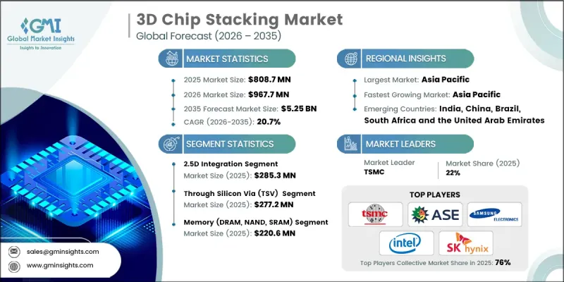
The Global 3D Chip Stacking Market was valued at USD 808.7 million in 2025 and is estimated to grow at a CAGR of 20.7% to reach USD 5.25 billion by 2035.
The market's expansion is fueled by rising demand for heterogeneous integration, cost optimization at advanced process nodes, AI and high-performance computing workload scaling, improved design flexibility, and ecosystem standardization through open interconnects. 3D chip stacking has become a cornerstone of modern semiconductor innovation, allowing multiple integrated circuit dies to be vertically stacked and interconnected within a single package. This approach reduces interconnect distances, accelerates signal transmission, enhances power efficiency, and enables a higher transistor density within compact footprints. Governments worldwide are actively supporting advanced packaging as part of industrial policies to strengthen domestic semiconductor capabilities and supply chain resilience. Technology is increasingly critical for AI accelerators, IoT devices, HPC platforms, and next-generation electronics that require high computational performance while maintaining low energy consumption and compact designs. As semiconductor ecosystems mature, 3D stacking is poised to be a key enabler of future electronics scalability and performance.
| Market Scope | |
|---|---|
| Start Year | 2025 |
| Forecast Year | 2026-2035 |
| Start Value | $808.7 Million |
| Forecast Value | $5.25 Billion |
| CAGR | 20.7% |
The 2.5D integration segment reached USD 285.3 million in 2025. 2.5D architectures place multiple dies side-by-side on an interposer, delivering high bandwidth, reduced latency, and enhanced interconnect density, which are essential for AI, HPC, networking, and graphics-intensive applications. The adoption of 2.5D integration is being reinforced by government-backed programs and R&D initiatives that accelerate interposer development and provide energy-efficient solutions for data centers and telecommunications infrastructure. Manufacturers are encouraged to invest in interposer-based 2.5D solutions to address high-bandwidth and low-latency requirements while leveraging policy support to advance next-generation semiconductor applications.
The through silicon via (TSV) segment generated USD 277.2 million in 2025. TSV technology enables vertical interconnects across stacked dies, reducing signal delay, improving power efficiency, and supporting thermal management, making it indispensable for AI accelerators, HPC systems, and data center memory stacks. Adoption of TSV is being reinforced by enterprise and government priorities to optimize chip density and performance while minimizing energy consumption and footprint. Manufacturers focusing on TSV-enabled high-performance memory and logic stacks are well-positioned to meet the increasing computational demands of AI and data-intensive applications while benefiting from government-sponsored R&D incentives.
North America 3D Chip Stacking Market accounted for 27.3% share in 2025. The region's rapid growth is supported by a mature technology ecosystem, strong R&D infrastructure, and rising demand from AI, automotive, and data center applications. Leading semiconductor companies, including Intel, NVIDIA, and AMD, are driving innovation in heterogeneous integration and high-density packaging. Government initiatives, such as funding programs for advanced packaging and 3D stacking, are enhancing domestic manufacturing capabilities and reducing dependence on overseas production. Companies in North America are scaling 3D stacking production lines in alignment with federal programs to capture high-performance computing, AI, and defense market opportunities.
Key players operating in the Global 3D Chip Stacking Market include TSMC, Intel Corporation, Samsung Electronics, Micron Technology, SK hynix, NVIDIA, Broadcom, Qualcomm, ASE Technology Holding, Amkor Technology, JCET Group, Powertech Technology Inc. (PTI), Sony Semiconductor Solutions, Toshiba (Kioxia Holdings), and Texas Instruments. Companies in the Global 3D Chip Stacking Market are strengthening their foothold by investing heavily in R&D for heterogeneous integration, high-density interposers, and TSV-enabled designs. Many firms are forming strategic alliances with foundries, memory suppliers, and AI platform developers to co-develop optimized chip architectures. Vertical integration strategies are being employed to enhance supply chain control and reduce production risks. Manufacturers are also focusing on government-backed initiatives to expand domestic manufacturing, improve thermal management solutions, and scale advanced packaging lines.
Table of Contents
Chapter 1 Methodology and Scope
- 1.1 Market scope and definition
- 1.2 Research design
- 1.2.1 Research approach
- 1.2.2 Data collection methods
- 1.3 Data mining sources
- 1.3.1 Global
- 1.3.2 Regional/Country
- 1.4 Base estimates and calculations
- 1.4.1 Base year calculation
- 1.4.2 Key trends for market estimation
- 1.5 Primary research and validation
- 1.5.1 Primary sources
- 1.6 Forecast model
- 1.7 Research assumptions and limitations
Chapter 2 Executive Summary
- 2.1 Industry 360° synopsis
- 2.2 Key market trends
- 2.2.1 Stacking architecture trends
- 2.2.2 Component trends
- 2.2.3 Technology trends
- 2.2.4 End-use industry trends
- 2.2.5 Application trends
- 2.2.6 Form factor trends
- 2.2.7 Regional trends
- 2.3 TAM Analysis, 2026 - 2035 (USD Million)
- 2.4 CXO perspectives: Strategic imperatives
Chapter 3 Industry Insights
- 3.1 Industry ecosystem analysis
- 3.1.1 Supplier landscape
- 3.1.2 Profit margin
- 3.1.3 Cost structure
- 3.1.4 Value addition at each stage
- 3.1.5 Factor affecting the value chain
- 3.1.6 Disruptions
- 3.2 Industry impact forces
- 3.2.1 Growth drivers
- 3.2.1.1 High demand for miniaturized and high-performance electronics
- 3.2.1.2 Increasing adoption of advanced packaging technologies
- 3.2.1.3 Rising use of 3D ICs in data centers and high-performance computing
- 3.2.1.4 Growth of AI, IoT, and automotive electronics applications
- 3.2.1.5 Expansion of semiconductor fabrication and foundry services
- 3.2.2 Pitfalls and challenges
- 3.2.2.1 High manufacturing complexity and cost
- 3.2.2.2 Thermal management and heat dissipation challenges
- 3.2.1 Growth drivers
- 3.3 Growth potential analysis
- 3.4 Regulatory landscape
- 3.4.1 North America
- 3.4.2 Europe
- 3.4.3 Asia Pacific
- 3.4.4 Latin America
- 3.4.5 Middle East & Africa
- 3.5 Porter’s analysis
- 3.6 PESTEL analysis
- 3.7 Technology and Innovation landscape
- 3.7.1 Current technological trends
- 3.7.2 Emerging technologies
- 3.8 Emerging Business Models
- 3.9 Compliance Requirements
Chapter 4 Competitive Landscape, 2025
- 4.1 Introduction
- 4.2 Company market share analysis
- 4.2.1 By region
- 4.2.1.1 North America
- 4.2.1.2 Europe
- 4.2.1.3 Asia Pacific
- 4.2.1.4 Latin America
- 4.2.1.5 Middle East & Africa
- 4.2.2 Market concentration analysis
- 4.2.1 By region
- 4.3 Competitive benchmarking of key players
- 4.3.1 Product portfolio comparison
- 4.3.1.1 Product range breadth
- 4.3.1.2 Technology
- 4.3.1.3 Innovation
- 4.3.2 Geographic presence comparison
- 4.3.2.1 Global footprint analysis
- 4.3.2.2 Service network coverage
- 4.3.2.3 Market penetration by region
- 4.3.3 Competitive positioning matrix
- 4.3.3.1 Leaders
- 4.3.3.2 Challengers
- 4.3.3.3 Followers
- 4.3.3.4 Niche players
- 4.3.1 Product portfolio comparison
- 4.4 Key developments, 2022-2025
- 4.4.1 Mergers and acquisitions
- 4.4.2 Partnerships and collaborations
- 4.4.3 Technological advancements
- 4.4.4 Expansion and investment strategies
- 4.4.5 Sustainability initiatives
- 4.4.6 Digital transformation initiatives
- 4.5 Emerging/ startup competitors landscape
Chapter 5 Market Estimates and Forecast, By Stacking Architecture, 2022 - 2035 (USD Million)
- 5.1 Key trends
- 5.2 Through-silicon via (TSV)
- 5.3 Micro-bump
- 5.4 Wafer-level packaging (WLP) based
- 5.5 Monolithic 3D
- 5.6 Hybrid
Chapter 6 Market Estimates and Forecast, By Component, 2022 - 2035 (USD Million)
- 6.1 Key trends
- 6.2 Memory (DRAM, NAND, SRAM)
- 6.3 Logic/processor
- 6.4 Interconnects
- 6.5 Thermal interface materials
- 6.6 Substrate & interposers
- 6.7 Others
Chapter 7 Market Estimates and Forecast, By Technology, 2022 - 2035 (USD Million)
- 7.1 Key Trends
- 7.2 2.5D integration
- 7.3 True 3D integration
- 7.4 Heterogeneous integration
- 7.5 Chiplet-based stacking
Chapter 8 Market Estimates and Forecast, By Form Factor, 2022 - 2035 (USD Million)
- 8.1 Key Trends
- 8.2 System-in-package (SiP)
- 8.3 Package-on-package (PoP)
- 8.4 3D die stack
- 8.5 Fan-out wafer level package (FOWLP)
- 8.6 Others
Chapter 9 Market Estimates and Forecast, By Application, 2022 - 2035 (USD Million)
- 9.1 Key Trends
- 9.2 High-performance computing (HPC)
- 9.3 Mobile & wearable devices
- 9.4 AI/ML accelerators
- 9.5 Storage systems
- 9.6 Baseband & RF systems
- 9.7 Sensors & MEMS
- 9.8 Others
Chapter 10 Market Estimates and Forecast, By End-use Industry, 2022 - 2035 (USD Million)
- 10.1 Key Trends
- 10.2 Consumer electronics
- 10.3 Telecommunications & networking
- 10.4 Automotive & transportation
- 10.5 Industrial & automation
- 10.6 Healthcare & medical devices
- 10.7 Aerospace & defense
- 10.8 Data centers & enterprise computing
- 10.9 Others
Chapter 11 Market Estimates and Forecast, By Region, 2022 - 2035 (USD Million)
- 11.1 Key trends
- 11.2 North America
- 11.2.1 U.S.
- 11.2.2 Canada
- 11.3 Europe
- 11.3.1 Germany
- 11.3.2 UK
- 11.3.3 France
- 11.3.4 Spain
- 11.3.5 Italy
- 11.3.6 Netherlands
- 11.4 Asia Pacific
- 11.4.1 China
- 11.4.2 India
- 11.4.3 Japan
- 11.4.4 Australia
- 11.4.5 South Korea
- 11.5 Latin America
- 11.5.1 Brazil
- 11.5.2 Mexico
- 11.5.3 Argentina
- 11.6 Middle East and Africa
- 11.6.1 Saudi Arabia
- 11.6.2 South Africa
- 11.6.3 UAE
Chapter 12 Company Profiles
- 12.1 Global Key Players
- 12.1.1 TSMC
- 12.1.2 Samsung Electronics
- 12.1.3 Intel Corporation
- 12.1.4 NVIDIA
- 12.1.5 Broadcom
- 12.2 Regional Key Players
- 12.2.1 North America
- 12.2.1.1 Micron Technology
- 12.2.1.2 Texas Instruments
- 12.2.1.3 Qualcomm
- 12.2.2 Asia Pacific
- 12.2.2.1 SK hynix
- 12.2.2.2 ASE Technology Holding
- 12.2.2.3 Amkor Technology
- 12.2.2.4 JCET Group
- 12.2.1 North America
- 12.3 Niche / Disruptors
- 12.3.1 Powertech Technology Inc. (PTI)
- 12.3.2 Sony Semiconductor Solutions
- 12.3.3 Toshiba (Kioxia Holdings)


