


 |
市場調查報告書
商品編碼
1721493
3D 堆疊市場機會、成長動力、產業趨勢分析及 2025 - 2034 年預測3D Stacking Market Opportunity, Growth Drivers, Industry Trend Analysis, and Forecast 2025 - 2034 |
||||||
2024 年全球 3D 堆疊市場價值為 18 億美元,預計到 2034 年將以 21.1% 的複合年成長率成長,達到 118 億美元。這一顯著成長主要歸因於對消費性電子產品、高效能運算系統和先進半導體技術不斷成長的需求。隨著人工智慧 (AI)、機器學習和物聯網 (IoT) 等資料密集型應用的不斷擴展,對更快的資料處理、更高的效率和更好的電源管理的需求變得比以往任何時候都更加重要。 3D 堆疊技術擴大被視為半導體創新的未來,它使設備製造商能夠透過在緊湊的空間內整合多個功能層(例如邏輯、記憶體和互連)來滿足這些不斷變化的需求。隨著電子產業在不影響效能的情況下不斷朝向小型化發展,3D 堆疊提供了實現更高吞吐量、更低延遲和卓越熱管理的理想途徑。從智慧型手機和穿戴式裝置到資料中心處理器和自動駕駛汽車,這項技術的應用範圍正在迅速擴大。基於小晶片的設計和異質整合的採用進一步推動了該市場的發展勢頭,為跨行業的特定用例客製化解決方案提供了靈活性。
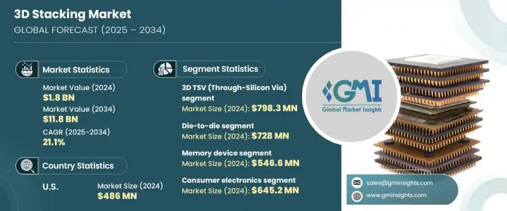
3D堆疊技術依互連方式可分為3D混合鍵結、3D矽通孔(TSV)、單晶片3D整合等。其中,3D TSV 部分在 2024 年創造了 7.983 億美元的收入。由於對支援資料中心、HPC 平台和自主系統效能要求的高速、低延遲記憶體介面的需求不斷成長,該部分正在經歷強勁成長。 5G 網路的推出和智慧型裝置的普及也加劇了對能夠管理大量即時資料處理的節能、緊湊晶片架構的需求。
| 市場範圍 | |
|---|---|
| 起始年份 | 2024 |
| 預測年份 | 2025-2034 |
| 起始值 | 18億美元 |
| 預測值 | 118億美元 |
| 複合年成長率 | 21.1% |
市場進一步依互連技術細分,包括晶片到晶圓、晶圓到晶圓、晶片到晶片、晶片到晶片和晶片到晶圓技術。 2024 年,晶片到晶片領域的價值為 7.28 億美元。這種方法對於需要晶片之間無縫通訊的多晶片模組和基於晶片組的架構尤其重要。它在推動人工智慧加速器、雲端基礎設施和 HPC 處理器方面發揮關鍵作用,提供了更大的設計靈活性、增強的節能效果和改進的可擴展性。
2024 年,美國 3D 堆疊市場產值達 4.86 億美元。由於對人工智慧應用、先進資料中心營運和 HPC 基礎設施的投資增加,該地區正在經歷大幅成長。美國半導體公司正在投入資源開發小晶片架構和基於 TSV 的設計,以突破下一代運算的效能、能源效率和可擴展性的界限。
全球 3D 堆疊市場的主要參與者包括 AMD、ASE Technology Holding、Amkor Technology、Broadcom、IBM、Intel、Graphcore、JCET Group、Marvell Technology、Micron Technology、Kioxia、NVIDIA、OmniVision Technologies、SK Hynix、Sony Semiconductor Solutions、Samsung EILlectronics、SPSPung EILlectin、Westx、Westx、Westx、Westx。這些公司正在加速晶片堆疊和互連方法的創新,以滿足人工智慧、資料中心和高效能運算市場日益成長的需求。透過專注的研發和策略性投資,他們旨在提供結合了功率效率、卓越性能和架構靈活性的面向未來的半導體解決方案。
目錄
第1章:方法論與範圍
第2章:執行摘要
第3章:行業洞察
- 產業生態系統分析
- 產業衝擊力
- 成長動力
- 對高效能運算(HPC)的需求不斷成長
- 擴展人工智慧和邊緣運算的應用
- 消費性電子產品的成長
- 汽車和物聯網應用增加
- 記憶體和儲存需求成長
- 產業陷阱與挑戰
- 製造成本高且複雜
- 散熱和電源管理問題
- 成長動力
- 成長潛力分析
- 監管格局
- 技術格局
- 未來市場趨勢
- 差距分析
- 波特的分析
- PESTEL分析
第4章:競爭格局
- 介紹
- 公司市佔率分析
- 主要市場參與者的競爭分析
- 競爭定位矩陣
- 策略儀表板
第5章:市場估計與預測:依方法,2021 年至 2034 年
- 主要趨勢
- 死對死
- 晶片到晶圓
- 晶圓對晶圓
- 晶片到晶片
- 晶片到晶圓
第6章:市場估計與預測:按互連技術,2021 年至 2034 年
- 主要趨勢
- 3D混合鍵合
- 3D TSV(矽通孔)
- 單晶片3D整合
第7章:市場估計與預測:按設備類型,2021 年至 2034 年
- 主要趨勢
- 邏輯積體電路
- 成像與光電子
- 儲存裝置
- MEMS/感測器
- 發光二極體
- 其他(射頻、光子學、類比和混合訊號以及功率裝置)
第8章:市場估計與預測:按最終用途產業,2021 年至 2034 年
- 主要趨勢
- 消費性電子產品
- 製造業
- 通訊(電信、資料中心和高效能運算)
- 汽車
- 醫療器材/醫療保健
- 其他(軍事與國防、航空
第9章:市場估計與預測:按地區,2021 年至 2034 年
- 主要趨勢
- 北美洲
- 美國
- 加拿大
- 歐洲
- 德國
- 英國
- 法國
- 西班牙
- 義大利
- 荷蘭
- 亞太地區
- 中國
- 印度
- 日本
- 澳洲
- 韓國
- 拉丁美洲
- 巴西
- 墨西哥
- 阿根廷
- 中東和非洲
- 沙烏地阿拉伯
- 南非
- 阿拉伯聯合大公國
第10章:公司簡介
- AMD
- Amkor Technology
- ASE Technology Holding
- Broadcom
- Graphcore
- IBM
- Intel
- JCET Group
- Kioxia
- Marvell Technology
- Micron Technology
- NVIDIA
- OmniVision Technologies
- Samsung Electronics
- SK Hynix
- Sony Semiconductor Solutions
- SPIL
- TSMC
- Western Digital
- Xilinx
The Global 3D Stacking Market was valued at USD 1.8 billion in 2024 and is expected to grow at a CAGR of 21.1% to reach USD 11.8 billion by 2034. This remarkable growth is largely attributed to the rising demand for consumer electronics, high-performance computing systems, and advanced semiconductor technologies. As data-intensive applications such as artificial intelligence (AI), machine learning, and the Internet of Things (IoT) continue to scale, the need for faster data processing, enhanced efficiency, and improved power management becomes more critical than ever. 3D stacking technology is increasingly seen as the future of semiconductor innovation, enabling device manufacturers to meet these evolving needs by integrating multiple functional layers-such as logic, memory, and interconnects-within a compact footprint. As the electronics industry pushes toward miniaturization without compromising performance, 3D stacking provides an ideal pathway to achieve higher throughput, lower latency, and superior thermal management. From smartphones and wearables to data center processors and autonomous vehicles, the scope of applications for this technology is rapidly expanding. The adoption of chiplet-based designs and heterogeneous integration further drives this market's momentum, offering the flexibility to customize solutions for specific use cases across industries.
3D stacking technology is classified based on interconnection methods, including 3D hybrid bonding, 3D Through-Silicon Via (TSV), and monolithic 3D integration. Among these, the 3D TSV segment generated USD 798.3 million in 2024. This segment is experiencing robust growth due to rising demand for high-speed, low-latency memory interfaces that support the performance requirements of data centers, HPC platforms, and autonomous systems. The rollout of 5G networks and the proliferation of smart devices are also intensifying the need for energy-efficient and compact chip architectures that can manage vast volumes of real-time data processing.
| Market Scope | |
|---|---|
| Start Year | 2024 |
| Forecast Year | 2025-2034 |
| Start Value | $1.8 Billion |
| Forecast Value | $11.8 Billion |
| CAGR | 21.1% |
The market is further segmented by interconnect technology, including die-to-wafer, wafer-to-wafer, die-to-die, chip-to-chip, and chip-to-wafer techniques. The die-to-die segment was valued at USD 728 million in 2024. This method is especially vital for multi-chip modules and chipset-based architectures that require seamless communication between dies. It plays a key role in advancing AI accelerators, cloud infrastructure, and HPC processors, offering greater design flexibility, enhanced energy savings, and improved scalability.
United States 3D Stacking Market generated USD 486 million in 2024. The region is witnessing substantial growth owing to increased investments in AI applications, advanced data center operations, and HPC infrastructure. US-based semiconductor firms are channeling resources into developing chiplet architectures and TSV-based designs to push the boundaries of performance, energy efficiency, and scalability in next-gen computing.
Key players in the Global 3D Stacking Market include AMD, ASE Technology Holding, Amkor Technology, Broadcom, IBM, Intel, Graphcore, JCET Group, Marvell Technology, Micron Technology, Kioxia, NVIDIA, OmniVision Technologies, SK Hynix, Sony Semiconductor Solutions, Samsung Electronics, SPIL, Western Digital, and Xilinx. These companies are accelerating innovations in chip stacking and interconnect methodologies to address the growing demand from AI, data center, and high-performance computing markets. Through focused R&D and strategic investments, they aim to deliver future-ready semiconductor solutions that combine power efficiency, superior performance, and architectural flexibility.
Table of Contents
Chapter 1 Methodology and Scope
- 1.1 Market scope and definitions
- 1.2 Research design
- 1.2.1 Research approach
- 1.2.2 Data collection methods
- 1.3 Base estimates and calculations
- 1.3.1 Base year calculation
- 1.3.2 Key trends for market estimation
- 1.4 Forecast model
- 1.5 Primary research and validation
- 1.5.1 Primary sources
- 1.5.2 Data mining sources
Chapter 2 Executive Summary
- 2.1 Industry 3600 synopsis
Chapter 3 Industry Insights
- 3.1 Industry ecosystem analysis
- 3.2 Industry impact forces
- 3.2.1 Growth drivers
- 3.2.1.1 Rising demand for high-performance computing (HPC)
- 3.2.1.2 Expanding applications in AI and edge computing
- 3.2.1.3 Growth in consumer electronics
- 3.2.1.4 Increase in automotive and IoT applications
- 3.2.1.5 Growth in memory and storage demand
- 3.2.2 Industry pitfalls and challenges
- 3.2.2.1 High manufacturing costs and complexity
- 3.2.2.2 Thermal and power management issues
- 3.2.1 Growth drivers
- 3.3 Growth potential analysis
- 3.4 Regulatory landscape
- 3.5 Technology landscape
- 3.6 Future market trends
- 3.7 Gap analysis
- 3.8 Porter’s analysis
- 3.9 PESTEL analysis
Chapter 4 Competitive Landscape, 2024
- 4.1 Introduction
- 4.2 Company market share analysis
- 4.3 Competitive analysis of major market players
- 4.4 Competitive positioning matrix
- 4.5 Strategy dashboard
Chapter 5 Market Estimates and Forecast, By Method, 2021 – 2034 (USD Million)
- 5.1 Key trends
- 5.2 Die-to-Die
- 5.3 Die-to-Wafer
- 5.4 Wafer-to-Wafer
- 5.5 Chip-to-Chip
- 5.6 Chip-to-Wafer
Chapter 6 Market Estimates and Forecast, By Interconnecting Technology, 2021 – 2034 (USD Million)
- 6.1 Key trends
- 6.2 3D hybrid bonding
- 6.3 3D TSV (Through-Silicon Via)
- 6.4 Monolithic 3D Integration
Chapter 7 Market Estimates and Forecast, By Device Type, 2021 – 2034 (USD Million)
- 7.1 Key trends
- 7.2 Logic ICs
- 7.3 Imaging & Optoelectronics
- 7.4 Memory devices
- 7.5 MEMS/Sensors
- 7.6 LEDs
- 7.7 Others (RF, photonics, analog & mixed signals, and power devices)
Chapter 8 Market Estimates and Forecast, By End Use Industry, 2021 – 2034 (USD Million)
- 8.1 Key trends
- 8.2 Consumer electronics
- 8.3 Manufacturing
- 8.4 Communications (Telecommunication, Data Centers & HPC)
- 8.5 Automotive
- 8.6 Medical Devices/Healthcare
- 8.7 Others (Military & Defence, Aviation)
Chapter 9 Market Estimates and Forecast, By Region, 2021 – 2034 (USD Million)
- 9.1 Key trends
- 9.2 North America
- 9.2.1 U.S.
- 9.2.2 Canada
- 9.3 Europe
- 9.3.1 Germany
- 9.3.2 UK
- 9.3.3 France
- 9.3.4 Spain
- 9.3.5 Italy
- 9.3.6 Netherlands
- 9.4 Asia Pacific
- 9.4.1 China
- 9.4.2 India
- 9.4.3 Japan
- 9.4.4 Australia
- 9.4.5 South Korea
- 9.5 Latin America
- 9.5.1 Brazil
- 9.5.2 Mexico
- 9.5.3 Argentina
- 9.6 Middle East and Africa
- 9.6.1 Saudi Arabia
- 9.6.2 South Africa
- 9.6.3 UAE
Chapter 10 Company Profiles
- 10.1 AMD
- 10.2 Amkor Technology
- 10.3 ASE Technology Holding
- 10.4 Broadcom
- 10.5 Graphcore
- 10.6 IBM
- 10.7 Intel
- 10.8 JCET Group
- 10.9 Kioxia
- 10.10 Marvell Technology
- 10.11 Micron Technology
- 10.12 NVIDIA
- 10.13 OmniVision Technologies
- 10.14 Samsung Electronics
- 10.15 SK Hynix
- 10.16 Sony Semiconductor Solutions
- 10.17 SPIL
- 10.18 TSMC
- 10.19 Western Digital
- 10.20 Xilinx


