


 |
市場調查報告書
商品編碼
2121339
影像感測器:市場佔有率分析、產業趨勢與統計、成長預測(2026-2031)Image Sensors - Market Share Analysis, Industry Trends & Statistics, Growth Forecasts (2026 - 2031) |
||||||

※ 本網頁內容可能與最新版本有所差異。詳細情況請與我們聯繫。
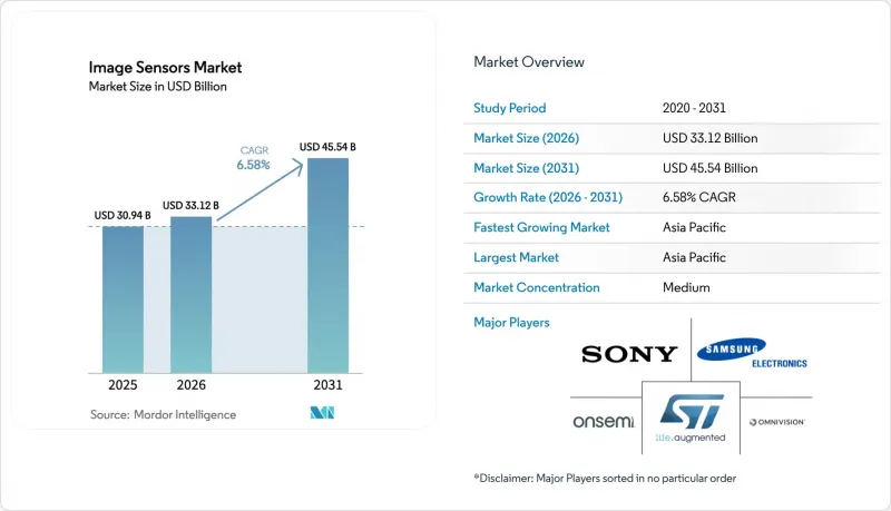
根據 Mordor Intelligence 預測,影像感測器市場規模將從 2025 年的 309.4 億美元成長到 2026 年的 331.2 億美元,到 2031 年將達到 455.4 億美元,2026 年至 2031 年的複合年預計成長率為 6.58%。
本報告按類型(CMOS 和 CCD)、處理技術(表面照明 (FSI)、背照式(BSI)、堆疊式 BSI)、百葉窗類型(捲簾百葉窗、全域百葉窗)、頻譜(可見光 (RGB)、近紅外線(NIR)、短波紅外線 (SWIR)、X光/ 15-124MP以上)、終端用戶產業(消費性電子、汽車與運輸、工業自動化與機器人、安防監控、其他)以及地區進行細分。市場預測以美元 (USD) 為單位。
全球影像感測器市場趨勢與洞察
多鏡頭智慧型手機的普及正在推動對CMOS感測器的需求。
預計到2025年,全球行動電話廠商將出貨12億部配備三個或更多後置相機的智慧型手機,年增26%。這主要歸功於超廣角和長焦鏡頭模組的普及,這些模組先前僅限於旗艦機型,如今也出現在中階機型中。激烈的市場競爭壓縮了零件成本,迫使感測器供應商接受更低的平均售價,同時將研發投入分散到大規模生產。像索尼和三星這樣擁有自有晶圓製造能力和影像訊號處理器(ISP)核心的垂直整合型公司,能夠保持盈利。隨著計算攝影技術的進步,價值中心正進一步從光學元件轉移到像素。諸如蘋果的「深度融合」(Deep Fusion)和Google的「夜視」(Night Sight)等演算法依賴高動態範圍和低讀出噪聲,因此,配備片上14位元轉換器、可實現120dB動態範圍的堆疊式背照式(BSI)晶片顯得尤為重要。
汽車全域百葉窗感知器,支援 L3 級或更高等級的 ADAS 系統
當車速超過100公里/小時時,滾動百葉窗造成的偽影將變得無法接受,促使汽車製造商(OEM)轉向使用全局百葉窗CMOS技術來製造前視和環景顯示攝影機。 2024年,梅賽德斯-賓士憑藉著八個全域百葉窗裝置,在德國和加州獲得了「Drive Pilot Level 3」認證。安森美半導體(ON Semiconductor)的Hyperlux平台整合了3微米像素和140dB的動態範圍,即使在高對比度場景下也能忠實地還原細節。即將實施的Euro NCAP 2025測試協議將強制要求幾乎所有車型配備行人偵測攝影機,這將加速全局百葉窗的普及。
300mm CIS晶圓產能瓶頸導致價格波動
2025年,影像感測器生產每月消耗18萬片300毫米晶圓,但需求超過供應8%,導致2025年初汽車感測器價格上漲12%。索尼投資2,000億日圓(約13.4億美元)擴建其熊本工廠,每月增加4萬片晶圓的產能,但新增產能要到2026年底才能投入運作。沒有長期合約的無晶圓廠供應商面臨著16週的前置作業時間和利潤率壓力。
細分市場分析
預計到2025年,CMOS元件將佔總銷售額的93.17%,這將鞏固規模經濟優勢,並推動影像感測器在市場佔有率上超越電荷耦合元件(CCD)。 CMOS將讀出電路、類比數位轉換器甚至神經加速器整合在同一晶片上,降低30%的組裝成本,並將功耗控制在500mW以下。 CCD在天文、病理學和醫用內視鏡領域佔據6.83%的市場佔有率,其亞電子級的讀出噪聲彌補了影格速率較低的不足。以索尼IMX661為代表的科學級CMOS,目前量子效率高達95%,讀出雜訊低於0.3e-,正在蠶食CCD的市佔率。短波紅外線 (SWIR) CMOS 目前僅佔市場的一小部分,但隨著工業和農業應用從矽 CCD 轉向砷化銦鎵 (InGaAs) 光電二極體,其市場佔有率正以每年 7.11% 的速度成長。
對於旨在實現10小時連續成像並最大限度降低暗電流的深空天文台而言,CCD仍然是最佳選擇。醫療影像公司看重CCD的均勻性,因為它能夠實現忠實的色彩還原和組織識別。然而,隨著科學儀器影像感測器的市場規模轉向雜訊水準低於0.5e-的堆疊式背照式CMOS,CCD的產量預計將會萎縮。小眾供應商將透過客製化生產維持生存,但行動電話、汽車和視覺系統等主流買家預計將圍繞先進的CMOS供應鏈進行整合。
預計到2025年,背照式技術將佔總銷售額的44.68%。然而,堆疊式背照感測器(BSI)正以7.34%的速度成長,因為廠商將動態隨機存取記憶體(DRAM)和人工智慧(AI)核心整合到光電二極體下方,從而將感測器轉變為超低延遲處理器。索尼的IMX989將45nm像素陣列堆疊在28nm邏輯晶片上,將影像到顯示的延遲從50ms降低到5ms,並支援14位元HDR成像。前照式CMOS仍應用於對價格敏感的後視攝影機,因為組件成本降低15%可以彌補靈敏度降低40%的不足。
隨著異質整合技術的日趨成熟,與堆疊式背照式影像感測器相關的市場規模預計將持續擴大。佳能的室溫表面活化鍵結技術可將背照式影像感測器的良率提高12個百分點,同時滿足汽車產業的缺陷容限標準。雖然穿透矽通孔(TSV)的形成增加了一道製程工序,成本也增加了8%,但OEM廠商願意接受這部分額外成本,因為該技術能夠在10mm見方的模組內實現多重曝光HDR、逐幀AI推理和鏡頭像差校正等功能。
區域分析
預計到2025年,亞太地區將佔全球銷售額的44.21%,並在2031年之前以7.65%的複合年成長率成長。中國組裝了全球68%的智慧型手機和52%的保全攝影機。儘管面臨出口限制的挑戰,本土感測器製造商仍擁有強大的市場優勢。日本的索尼和佳能憑藉堆疊式背照式感測器(BSI)和科學級CMOS感測器,繼續佔據全球高階市場一半的佔有率;而韓國的三星則憑藉其堆疊式LPDDR5記憶體技術,突破了8K錄影的瓶頸。
歐洲和北美佔總銷售額的38%。將於2024年7月生效的歐盟通用安全法規(GSR)強制要求車輛配備自動緊急煞車和車道維持輔助系統,這將導致攝影機安裝數量的增加。意法半導體(STMicroelectronics)和歐司朗(ams OSRAM)已在歐洲建立了強大的業務基礎,供應符合AEC-Q100標準的感測器,這些感測器可在-40°C至+105°C的溫度範圍內工作。在北美市場,特斯拉的12攝影機「完全自動駕駛」系統和亞馬遜的5萬台視覺引導機器人佔據主導地位。
中東、非洲和南美洲佔剩餘的18%。杜拜、利雅德和杜哈等城市部署了智慧城市邊緣視覺技術,沙烏地阿拉伯的NEOM新城訂購了價值3億美元的10萬台人工智慧攝影機。南非礦場在自動駕駛運輸卡車上部署了熱成像器,巴西農產品測試並部署了相容短波紅外線(SWIR)的灌溉系統。基礎設施限制和外匯波動阻礙了技術的快速普及,但企劃為基礎的激增正在形成區域性的需求高峰。
其他好處
- Excel格式的市場預測(ME)表
- 3個月的分析師支持
目錄
第1章:引言
- 研究假設和市場定義
- 調查範圍
第2章:調查方法
第3章執行摘要
第4章 市場狀況
- 市場概覽
- 市場促進因素
- 多鏡頭智慧型手機的普及正在推動對CMOS感測器的需求。
- 汽車全域百葉窗感知器,支援 L3 級或更高等級的 ADAS 系統
- 利用邊緣人工智慧視覺模組加速智慧城市投資
- SWIR感測器在精密農業和工業品管領域的應用
- 支援下一代AR/VR穿戴裝置的3D和事件驅動型感測器
- 由於政府安全法規,車載動態監視器數量激增。
- 市場限制因素
- 300mm CIS晶圓產能瓶頸導致價格波動
- 由於像素尺寸小於 1µm 時的熱雜訊限制,解析度競爭陷入停滯。
- 對先進成像晶片的出口限制影響中國原始設備製造商
- 短波紅外線感測器的高整合成本正在減緩消費者對其的接受度。
- 產業價值鏈分析
- 監理展望
- 技術展望
- 波特五力分析
- 宏觀經濟因素對市場的影響
第5章 市場規模與成長預測
- 按類型
- CMOS
- CCD
- 透過加工技術
- 前照式(FSI)
- 背照式(BSI)
- 堆疊式BSI
- 按百葉窗類型
- 百葉窗
- 全球百葉窗
- 頻譜類型
- 可見光(RGB)
- 近紅外線(NIR)
- 短波紅外線(SWIR)
- X光/紫外線
- 通過決議
- 小於100萬像素
- 1~3MP
- 4~12MP
- 13~24MP
- 2500萬像素或以上
- 按最終用戶行業分類
- 家用電子產品
- 汽車和運輸業
- 工業自動化機器人
- 安全監控
- 醫療保健和生命科學
- 航太/國防
- 智慧城市、農業、海洋
- 按地區
- 北美洲
- 美國
- 加拿大
- 墨西哥
- 歐洲
- 英國
- 德國
- 法國
- 義大利
- 其他歐洲國家
- 亞太地區
- 中國
- 日本
- 印度
- 韓國
- 其他亞太國家
- 中東
- 以色列
- 沙烏地阿拉伯
- 阿拉伯聯合大公國
- 土耳其
- 其他中東國家
- 非洲
- 南非
- 埃及
- 其他非洲國家
- 南美洲
- 巴西
- 阿根廷
- 南美洲其他地區
- 北美洲
第6章 競爭情勢
- 市場集中度
- 策略趨勢
- 市佔率分析
- 公司簡介
- Sony Group Corp.
- Samsung Electronics Co., Ltd.
- OmniVision Technologies, Inc.
- STMicroelectronics NV
- ON Semiconductor Corporation
- Canon Inc.
- Panasonic Holdings Corporation
- Teledyne DALSA Inc.
- ams OSRAM AG
- SK hynix Inc.
- GalaxyCore Inc.
- Hamamatsu Photonics KK
- SmartSens Technology
- PixArt Imaging Inc.
- Himax Technologies, Inc.
- Tower Semiconductor Ltd.
- Teledyne e2v
- Gpixel Inc.
- Forza Silicon Corp.
- Toshiba Electronic Devices and Storage Corp.
- Pyxalis SA
第7章 市場機會與未來展望
According to Mordor Intelligence, the image sensors market size is expected to increase from USD 30.94 billion in 2025 to USD 33.12 billion in 2026 and reach USD 45.54 billion by 2031, growing at a CAGR of 6.58% over 2026-2031.
This report is Segmented by Type (CMOS, and CCD), Processing Technology (FSI, BSI, and Stacked BSI), Shutter Type (Rolling, and Global), Spectrum (Visible, NIR, SWIR, and X-ray/UV), Resolution (Less Than 1 MP, 1-3 MP, 4-12 MP, 13-24 MP, and >=25 MP), End-User (Consumer Electronics, Automotive, Industrial, Security, Healthcare, and More), and Geography. Market Forecasts are Provided in Terms of Value (USD).
Global Image Sensors Market Trends and Insights
Smartphone Multicamera Proliferation Elevating CMOS Demand
Global handset vendors shipped 1.2 billion smartphones with three or more rear cameras in 2025, up 26% year-on-year, as mid-tier models adopted ultra-wide and telephoto modules once reserved for flagships. Competitive pressure compressed the bill of materials, forcing sensor suppliers to spread R&D across massive volumes while conceding lower average selling prices. Vertically integrated players such as Sony and Samsung, with captive wafer capacity and image-signal-processor (ISP) cores, are positioned to sustain profitability. Computational photography further shifts value from optics to pixels; algorithms like Apple Deep Fusion and Google Night Sight rely on high dynamic range and low read noise, placing a premium on stacked BSI chips with on-chip 14-bit converters that deliver 120 dB dynamic range.
Automotive-Grade Global-Shutter Sensors Enabling Level 3+ ADAS
Rolling-shutter artifacts become unacceptable when vehicles travel above 100 km/h, prompting OEMs to switch to global-shutter CMOS for forward-facing and surround-view cameras. Mercedes-Benz certified Drive Pilot Level 3 in Germany and California in 2024 using eight global-shutter devices. ON Semiconductor's Hyperlux platform integrates 3 µm pixels with 140 dB dynamic range, preserving detail in high-contrast scenes. Euro NCAP's 2025 test protocols effectively require pedestrian-detection cameras on all models, accelerating global-shutter penetration.
300 mm CIS Wafer Capacity Bottlenecks Creating Price Volatility
Image sensors consumed 180,000 300 mm wafer starts per month in 2025, yet demand exceeded supply by 8%, inflating automotive-grade sensor prices by 12% in early 2025. Sony allocated JPY 200 billion (USD 1.34 billion) to expand its Kumamoto fab by 40,000 wafers per month, but the additional capacity arrives only in late 2026. Fabless vendors lacking long-term contracts face 16-week lead times and margin pressure.
Other drivers and restraints analyzed in the detailed report include:
- Edge-AI Vision Modules Catalysing Smart-City Investments
- SWIR Sensors Penetrating Precision Agriculture and Industrial QC
- Thermal Noise Limits in Sub-1 µm Pixels Hindering Resolution Race
For complete list of drivers and restraints, kindly check the Table Of Contents.
Segment Analysis
CMOS devices captured 93.17% of 2025 revenue, a footprint that cements scale economies and drives the image sensors market share advantage over charge-coupled devices (CCD). CMOS integrates readout, analog-to-digital converters, and even neural accelerators on the same die, trimming assembly cost by 30% and power budgets below 500 mW. CCD held 6.83% share in astronomy, pathology, and medical endoscopy, where its sub-electron read noise outweighs slower frame rates. Scientific CMOS, typified by Sony's IMX661, now delivers 95% quantum efficiency and read noise under 0.3 e-, eroding CCD's niche. SWIR CMOS, while a small subset today, is expanding 7.11% per year as industrial and agricultural applications migrate from silicon CCD to indium-gallium-arsenide photodiodes.
CCD remains the tool of choice for deep-sky observatories seeking 10-hour integrations with minimal dark current. Medical imaging firms prize CCD uniformity for colour-true tissue differentiation. Yet as the image sensors market size for scientific devices shifts to stacked BSI CMOS with sub-0.5 e- noise, CCD volume is forecast to contract. Niche suppliers will survive on bespoke runs, but mainstream handset, automotive, and vision-system buyers will consolidate around advanced CMOS supply chains.
Backside-illuminated technologies owned 44.68% of revenue in 2025. However, stacked BSI is advancing at 7.34% as vendors embed dynamic random-access memory (DRAM) and AI cores under the photodiodes, converting sensors into ultra-low-latency processors. Sony's IMX989 stacks a 45 nm pixel array atop a 28 nm logic die, cutting image-to-display latency from 50 ms to 5 ms and enabling 14-bit HDR capture. Front-side-illuminated CMOS remains in price-sensitive rear-view cameras, where a 15% bill-of-materials saving still outweighs the 40% sensitivity penalty.
The image sensors market size linked to stacked BSI will keep expanding as heterogeneous integration matures. Canon's room-temperature surface-activated bonding raises BSI yields by 12 points while meeting automotive defect thresholds. Although through-silicon-via formation adds process steps and 8% cost, OEMs accept the premium for multi-exposure HDR, per-frame AI inference, and lens aberration correction delivered within a 10 mm-square module.
Complete Report Scope:
- By Type
- CMOS
- CCD
- By Processing Technology
- Front-Side Illuminated (FSI)
- Back-Side Illuminated (BSI)
- Stacked BSI
- By Shutter Type
- Rolling Shutter
- Global Shutter
- By Spectrum
- Visible (RGB)
- Near-Infrared (NIR)
- Short-Wave Infrared (SWIR)
- X-ray / Ultraviolet
- By Resolution
- Less than 1 MP
- 1 - 3 MP
- 4 - 12 MP
- 13 - 24 MP
- More than Equal to 25 MP
- By End-User Industry
- Consumer Electronics
- Automotive and Transportation
- Industrial Automation and Robotics
- Security and Surveillance
- Healthcare and Life Sciences
- Aerospace and Defense
- Smart City, Agriculture, Marine
- By Geography
- North America
- United States
- Canada
- Mexico
- Europe
- United Kingdom
- Germany
- France
- Italy
- Rest of Europe
- Asia-Pacific
- China
- Japan
- India
- South Korea
- Rest of Asia-Pacific
- Middle East
- Israel
- Saudi Arabia
- United Arab Emirates
- Turkey
- Rest of Middle East
- Africa
- South Africa
- Egypt
- Rest of Africa
- South America
- Brazil
- Argentina
- Rest of South America
- North America
Geography Analysis
Asia-Pacific contributed 44.21% of 2025 revenue and is projected to grow 7.65% CAGR to 2031. China assembled 68% of smartphones and 52% of security cameras, giving local sensor firms a home-field advantage despite export-control headwinds. Japan's Sony and Canon retained half of global premium revenue from stacked BSI and scientific CMOS, while South Korea's Samsung leveraged LPDDR5 memory stacking to break 8K recording barriers.
Europe and North America pooled 38% of revenue. The European Union's General Safety Regulation, effective July 2024, mandates automated emergency braking and lane-keeping assist, lifting camera content. STMicroelectronics and ams OSRAM supply AEC-Q100 sensors that operate from -40 °C to +105 °C, anchoring a defensible European franchise. North American momentum splits between Tesla's 12-camera Full Self-Driving suite and Amazon's 50,000 vision-guided robots.
The Middle East, Africa, and South America captured the remaining 18%. Dubai, Riyadh, and Doha rolled out smart-city edge vision, while Saudi Arabia's NEOM ordered 100,000 AI cameras worth USD 300 million. South Africa's mines deployed thermal imagers on autonomous haul trucks, and Brazil's agribusiness tested SWIR-enabled irrigation. Infrastructure constraints and foreign-exchange volatility temper accelerated uptake, but project-based spikes create localized demand peaks.
- Sony Group Corp.
- Samsung Electronics Co., Ltd.
- OmniVision Technologies, Inc.
- STMicroelectronics N.V.
- ON Semiconductor Corporation
- Canon Inc.
- Panasonic Holdings Corporation
- Teledyne DALSA Inc.
- ams OSRAM AG
- SK hynix Inc.
- GalaxyCore Inc.
- Hamamatsu Photonics K.K.
- SmartSens Technology
- PixArt Imaging Inc.
- Himax Technologies, Inc.
- Tower Semiconductor Ltd.
- Teledyne e2v
- Gpixel Inc.
- Forza Silicon Corp.
- Toshiba Electronic Devices and Storage Corp.
- Pyxalis S.A.
Additional Benefits:
- The market estimate (ME) sheet in Excel format
- 3 months of analyst support
TABLE OF CONTENTS
1 INTRODUCTION
- 1.1 Study Assumptions and Market Definition
- 1.2 Scope of the Study
2 RESEARCH METHODOLOGY
3 EXECUTIVE SUMMARY
4 MARKET LANDSCAPE
- 4.1 Market Overview
- 4.2 Market Drivers
- 4.2.1 Smartphone Multicamera Proliferation Elevating CMOS Demand
- 4.2.2 Automotive-Grade Global-Shutter Sensors Enabling Level-3+ ADAS
- 4.2.3 Edge-AI Vision Modules Catalysing Smart-City Investments
- 4.2.4 SWIR Sensors Penetrating Precision-Agriculture And Industrial QC
- 4.2.5 3D/Event-Based Sensors Powering Next-Gen AR/VR Wearables
- 4.2.6 Government Safety Mandates Driving In-Cabin DMS Cameras
- 4.3 Market Restraints
- 4.3.1 300 mm CIS Wafer Capacity Bottlenecks Creating Price Volatility
- 4.3.2 Thermal Noise Limits in Sub-1 µm Pixels Hindering Resolution Race
- 4.3.3 Export Controls on Advanced Imaging Chips Impacting Chinese OEMs
- 4.3.4 High Integration Cost of SWIR Sensors Slowing Consumer Uptake
- 4.4 Industry Value-Chain Analysis
- 4.5 Regulatory Outlook
- 4.6 Technological Outlook
- 4.7 Porter's Five Forces Analysis
- 4.7.1 Bargaining Power of Suppliers
- 4.7.2 Bargaining Power of Consumers
- 4.7.3 Threat of New Entrants
- 4.7.4 Threat of Substitutes
- 4.7.5 Intensity of Competitive Rivalry
- 4.8 Impact of Macroeconomic Factors on the Market
5 MARKET SIZE AND GROWTH FORECASTS (VALUE)
- 5.1 By Type
- 5.1.1 CMOS
- 5.1.2 CCD
- 5.2 By Processing Technology
- 5.2.1 Front-Side Illuminated (FSI)
- 5.2.2 Back-Side Illuminated (BSI)
- 5.2.3 Stacked BSI
- 5.3 By Shutter Type
- 5.3.1 Rolling Shutter
- 5.3.2 Global Shutter
- 5.4 By Spectrum
- 5.4.1 Visible (RGB)
- 5.4.2 Near-Infrared (NIR)
- 5.4.3 Short-Wave Infrared (SWIR)
- 5.4.4 X-ray / Ultraviolet
- 5.5 By Resolution
- 5.5.1 Less than 1 MP
- 5.5.2 1 - 3 MP
- 5.5.3 4 - 12 MP
- 5.5.4 13 - 24 MP
- 5.5.5 More than Equal to 25 MP
- 5.6 By End-User Industry
- 5.6.1 Consumer Electronics
- 5.6.2 Automotive and Transportation
- 5.6.3 Industrial Automation and Robotics
- 5.6.4 Security and Surveillance
- 5.6.5 Healthcare and Life Sciences
- 5.6.6 Aerospace and Defense
- 5.6.7 Smart City, Agriculture, Marine
- 5.7 By Geography
- 5.7.1 North America
- 5.7.1.1 United States
- 5.7.1.2 Canada
- 5.7.1.3 Mexico
- 5.7.2 Europe
- 5.7.2.1 United Kingdom
- 5.7.2.2 Germany
- 5.7.2.3 France
- 5.7.2.4 Italy
- 5.7.2.5 Rest of Europe
- 5.7.3 Asia-Pacific
- 5.7.3.1 China
- 5.7.3.2 Japan
- 5.7.3.3 India
- 5.7.3.4 South Korea
- 5.7.3.5 Rest of Asia-Pacific
- 5.7.4 Middle East
- 5.7.4.1 Israel
- 5.7.4.2 Saudi Arabia
- 5.7.4.3 United Arab Emirates
- 5.7.4.4 Turkey
- 5.7.4.5 Rest of Middle East
- 5.7.5 Africa
- 5.7.5.1 South Africa
- 5.7.5.2 Egypt
- 5.7.5.3 Rest of Africa
- 5.7.6 South America
- 5.7.6.1 Brazil
- 5.7.6.2 Argentina
- 5.7.6.3 Rest of South America
- 5.7.1 North America
6 COMPETITIVE LANDSCAPE
- 6.1 Market Concentration
- 6.2 Strategic Moves
- 6.3 Market Share Analysis
- 6.4 Company Profiles (includes Global Level Overview, Market Level Overview, Core Segments, Financials as available, Strategic Information, Market Rank/Share, Products and Services, Recent Developments)
- 6.4.1 Sony Group Corp.
- 6.4.2 Samsung Electronics Co., Ltd.
- 6.4.3 OmniVision Technologies, Inc.
- 6.4.4 STMicroelectronics N.V.
- 6.4.5 ON Semiconductor Corporation
- 6.4.6 Canon Inc.
- 6.4.7 Panasonic Holdings Corporation
- 6.4.8 Teledyne DALSA Inc.
- 6.4.9 ams OSRAM AG
- 6.4.10 SK hynix Inc.
- 6.4.11 GalaxyCore Inc.
- 6.4.12 Hamamatsu Photonics K.K.
- 6.4.13 SmartSens Technology
- 6.4.14 PixArt Imaging Inc.
- 6.4.15 Himax Technologies, Inc.
- 6.4.16 Tower Semiconductor Ltd.
- 6.4.17 Teledyne e2v
- 6.4.18 Gpixel Inc.
- 6.4.19 Forza Silicon Corp.
- 6.4.20 Toshiba Electronic Devices and Storage Corp.
- 6.4.21 Pyxalis S.A.
7 MARKET OPPORTUNITIES AND FUTURE OUTLOOK
- 7.1 White-Space and Unmet-Need Assessment

 車載監控系統市場預測至2034年-全球分析(依系統類型、組件、駕駛監控功能、乘員監控功能、車輛類型、車輛等級、驅動系統、應用、最終用戶及地區分類)
 安防應用的影像感測器:市場佔有率分析、產業趨勢與統計及成長預測(2026-2031 年)歐洲影像感測器:市場佔有率分析、產業趨勢與統計及成長預測(2026-2031)
 影像感測器市場:2026-2032年全球市場預測(按感測器類型、光譜範圍、影像解析度、處理方法、終端用戶產業和分銷管道分類)影像感測器市場預測至2034年-全球技術、頻譜、處理方法、陣列方法、解析度、百葉窗方法、封裝方法、終端應用產業及區域分析
 全球影像感測器市場(至2032年):按類型、處理方法、頻譜、陣列、解析度和應用分類
 InGaAs影像感測器市場-全球產業規模、佔有率、趨勢、機會、預測:按類型、波長、應用、最終用戶、地區和競爭格局分類,2021-2031年
 模組化低光感測器市場報告:趨勢、預測和競爭分析(至2035年)影像感測器市場預測至2034年—頻譜、處理方法、技術、最終用戶和地區分類的全球分析
 車內監控(DMS、OMS)市場(2026 年)