


 |
市場調查報告書
商品編碼
2115921
SRAM 和 ROM 設計 IP:市場佔有率分析、行業趨勢和統計數據、成長預測(2026-2031 年)SRAM And ROM Design IP - Market Share Analysis, Industry Trends & Statistics, Growth Forecasts (2026 - 2031) |
||||||

※ 本網頁內容可能與最新版本有所差異。詳細情況請與我們聯繫。
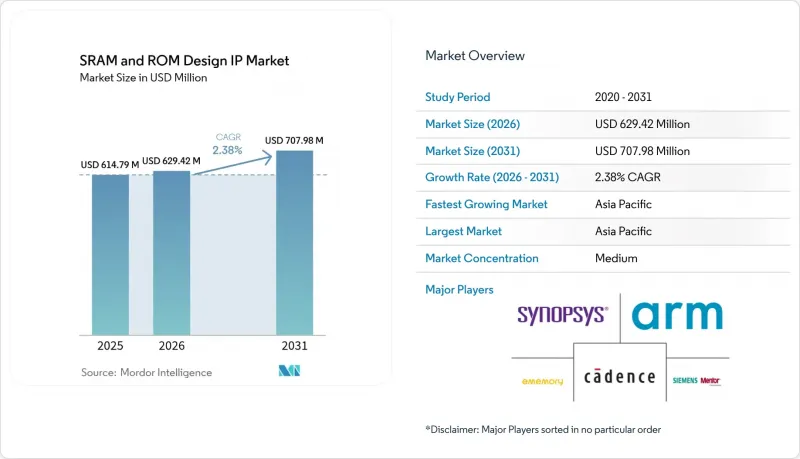
據 Mordor Intelligence 稱,2025 年 SRAM 和 ROM 設計 IP 的市場規模為 6.1479 億美元,預計到 2031 年將達到 7.0798 億美元,而 2026 年為 6.2942 億美元,預測期(2026-2031 年)的複合年成長率為 2.38%。
本報告按記憶體類型(SRAM、ROM 及其他)、應用領域(家用電子電器、通訊與網路及其他)、製程節點(14nm 或更低、15-22nm、28-40nm、45nm 及以上)、IP 交付方式(硬 IP、軟 IP 及其他)以及地區(北美、南美、歐洲、亞太地區、中東和非洲)進行細分。市場預測以美元 (USD) 為單位。
全球SRAM/ROM設計IP市場趨勢及洞察
需要大規模片上快取的以人工智慧為中心的SoC的激增。
目前,推理加速器整合了高達 40 MB 的 SRAM 來存儲權重和特徵圖,遠遠超過通用處理器中常見的 8-16 MB。 「記憶體運算」方法將算術運算直接置於位元單元內,以降低資料傳輸相關的能耗,這對編譯器提出了新的要求。此外,正在多個地區推進的「自主人工智慧」舉措透過資助國內晶片開發項目來擴大市場,這些項目強制要求使用本地檢驗的記憶體 IP。3D穿透矽通孔(TSV) 技術在保持緊湊尺寸的同時,進一步提高了快取容量。能夠提供具有全面時序特性的多吉赫、低漏電流 SRAM 巨集單元的供應商,最有可能抓住這一市場繁榮的機會。
5G 和邊緣運算的部署正在加速低功耗嵌入式 SRAM 的採用。
邊緣伺服器和物聯網節點需要工作電壓低於 1V 的記憶體模組,能夠在 -40 度C至 125 度C的溫度範圍內保持資料穩定。新一代 IP 結合了多閾值電晶體和功率門控單元,可將漏電流控制在每兆位元 1 奈安以下。動態體偏壓技術使設計人員能夠以微分增量平衡待機功耗和存取速度。同時,5G基頻ASIC 採用雙埠 SRAM,並針對突發封包的緩衝進行了精細調整。這些嚴格的功耗要求提高了特性深度和臨界點檢驗標準的門檻,因此,擁有跨多家代工廠的矽驗證資料的供應商更具優勢。
開放原始碼記憶體編譯器的價格壓力正在降低平均售價(ASP)。
RISC-V 生態系統內的社群計畫現在為成熟節點提供免費的 SRAM 產生器,為對成本敏感的穿戴式裝置和玩具市場提供了比商業產品更低成本的替代方案。大學也在進一步推動庫的開發,幫助無廠半導體公司快速實現其首個晶片的誕生。供應商正努力透過強調降低漏電流、覆蓋死角和安全封裝來維持利潤率——這些特性在開放原始碼流程中往往缺失。儘管如此,入門級產品的收入來源仍在持續萎縮。
細分市場分析
2025年,SRAM在SRAM/ROM設計IP市場中仍將維持60.05%的市佔率。這充分展現了SRAM作為快取和緩衝區時無與倫比的速度優勢。隨著AI加速器和5G交換器對更大片上空間的需求,該細分市場的絕對值正在穩步成長。同時,作為啟動程式碼和校準表的ROM系列(包括PROM、EPROM和EEPROM)正隨著系統晶片(SoC)整合化而逐漸縮小,因為獨立模組被淘汰。與MRAM和其他新興非揮發性記憶體相關的SRAM/ROM設計IP市場規模仍然小規模,但隨著eFlash在28nm及以下製程達到容量極限,其市場地位預計將會增強。
與嵌入式快閃記憶體和替代性非揮發性記憶體 (NVM) 相關的授權業務正以 3.72% 的複合年成長率 (CAGR) 高速成長,這主要得益於物聯網微控制器和汽車電子控制單元 (ECU) 對高耐久性程式碼儲存的需求。結合了 SRAM 的速度和 MRAM 的非揮發性的多技術編譯器,正在支援已進入試生產階段的混合陣列。精通兩種揮發性記憶體領域的供應商能夠獲得更高的價格溢價,尤其是在他們能夠跨流程映射相同的邏輯介面並降低韌體移植風險的情況下。
到2025年,家用電子電器將佔據SRAM/ROM設計IP市場佔有率的36.10%,這主要得益於智慧型手機、平板電腦和遊戲機對日益先進的圖形處理和本地AI功能的需求。儘管設計週期依然活躍,但隨著廠商將基板空間重新用於攝影機和天線,產能成長已趨於平緩。通訊ASIC依賴於針對亞奈秒延遲最佳化的雙埠SRAM來維持線速封包傳輸,而編譯器柔軟性在這一細分市場中至關重要。
預計到2031年,汽車和運輸機械行業的IP訂單將以4.9%的複合年成長率成長,這主要得益於對高級駕駛輔助系統(ADAS)的需求,這些系統需要具備ASIL-D診斷功能的多GB片上陣列。因此,符合1級功能安全要求的SRAM和ROM設計IP的市場規模成長速度超過其他任何產業。雖然航太和國防領域的需求仍然較小,但抗輻射加強的IP庫需要嚴格的認證流程,因此平均售價較高。
區域分析
預計到2025年,亞太地區將佔SRAM/ROM設計IP市場收入的46.85%,並在2031年之前以3.82%的複合年成長率成長。台灣、韓國和中國當地的晶圓代工叢集正在降低流片成本,而國家補貼計畫則支持國內編譯器開發計畫。日本正透過提供專為一級汽車零件供應商和工業機器人量身定做的安全型宏來擴大該地區的市場佔有率。
北美佔據了尖端設計項目的大部分佔有率,矽谷新創公司和超大規模雲端供應商競相推出各自的人工智慧晶片。 《晶片法案》(CHIPS Act)正在吸引新的資本流入美國本土晶圓廠,促進國內智慧財產權檢驗實驗室的建立,並為中小企業開闢獲得津貼的途徑。一家底特律的一級汽車供應商正與航太產業的主要企業合作,透過要求提供抗輻射加固且符合ASIL-D標準的宏晶片,進軍高利潤的細分市場。
歐洲正著力發展汽車和工業自動化,充分利用德國的OEM生態系統和ISO 26262標準的嚴格執行。北歐國家為嚴苛環境提供超低功耗記憶體,而法國和義大利則在探索優先考慮自身智慧財產權的自主運算計畫。整體而言,歐洲大陸的需求往往更注重可靠性和功能安全認證,而非簡單的整合密度。
其他好處:
- Excel格式的市場預測(ME)表
- 3個月的分析師支持
目錄
第1章:引言
- 市場分析與定義的前提條件
- 分析範圍
第2章 分析方法
第3章執行摘要
第4章 市場狀況
- 市場概覽
- 市場促進因素
- 需要大規模片上快取的以人工智慧為中心的SoC的激增。
- 5G 和邊緣運算的日益普及正在加速低功耗嵌入式 SRAM 的採用。
- 從 28nm 或更小的 eFlash 轉向 MRAM 的轉變將開啟新的授權收入來源。
- 汽車一級功能安全標準正在推動對認證記憶體 IP 的需求。
- 晶片組架構規範了晶片間記憶體 IP 的要求。
- 晶圓代工廠提供的承包式記憶體編譯器程式正在縮短無廠半導體公司的產品上市時間。
- 市場限制因素
- 開放原始碼記憶體編譯器的價格壓力正在拉低平均售價(ASP)。
- 新興的 ReRAM/FeRAM 替代技術正在蠶食小規模ROM IP 插槽的市場。
- 中國流片生產過程中出口管制合規的障礙
- 7nm SRAM 位元單元的可靠性問題導致認證成本上升。
- 產業生態系分析
- 宏觀經濟因素的影響
- 技術展望
- 波特五力分析
第5章:預測市場規模與成長率
- 按記憶體類型
- SRAM
- ROM(PROM/EPROM/EEPROM)
- MRAM
- 嵌入式快閃記憶體/其他非揮發性記憶體
- 透過使用
- 家用電子電器
- 通訊與網路
- 汽車和運輸業
- 工業物聯網
- 航太/國防
- 其他用途
- 依技術節點
- 14奈米或更小
- 15~22 nm
- 28~40 nm
- 45奈米或以上
- 透過 IP 提供方式
- 硬IP
- 軟IP
- 參數化編譯器 IP
- 晶片級/3D晶片級IP
- 按地區
- 北美洲
- 美國
- 加拿大
- 墨西哥
- 南美洲
- 巴西
- 阿根廷
- 其他南美國家
- 歐洲
- 德國
- 英國
- 法國
- 義大利
- 西班牙
- 其他歐洲國家
- 亞太地區
- 中國
- 日本
- 印度
- 韓國
- 東南亞
- 其他亞太國家
- 中東
- 沙烏地阿拉伯
- 阿拉伯聯合大公國
- 土耳其
- 其他中東國家
- 非洲
- 南非
- 奈及利亞
- 其他非洲國家
- 北美洲
第6章 競爭情勢
- 市場集中度
- 策略趨勢
- 市佔率分析
- 公司簡介
- Arm Ltd.
- Synopsys Inc.
- Cadence Design Systems Inc.
- Siemens EDA(Mentor Graphics Corporation)
- eMemory Technology Inc.
- Silvaco Inc.
- Dolphin Design SAS
- VeriSilicon Holdings Co. Ltd.
- SureCore Ltd.
- Xilinx Inc.
- Renesas Electronics Corporation
- Everspin Technologies Inc.
- Avalanche Technology Inc.
- TDK Corporation
- Kilopass Technology Inc.
- Silicon Storage Technology Inc.
- GSI Technology Inc.
- Dolphin Technology Inc.
- TekStart LLC
- Flex Logix Technologies Inc.
- Rambus Inc.
第7章 市場機會與未來展望
According to Mordor Intelligence, the SRAM and ROM Design IP market size was valued at USD 614.79 million in 2025 and estimated to grow from USD 629.42 million in 2026 to reach USD 707.98 million by 2031, at a CAGR of 2.38% during the forecast period (2026-2031).
This report is Segmented by Memory Type (SRAM, ROM, and More), Application (Consumer Electronics, Telecommunications and Networking, and More), Technology Node (<=14nm, 15-22nm, 28-40nm, and >=45nm), IP Delivery Type (Hard IP, Soft IP, and More), and Geography (North America, South America, Europe, Asia Pacific, Middle East, and Africa). The Market Forecasts are Provided in Terms of Value (USD).
Global SRAM And ROM Design IP Market Trends and Insights
Proliferation of AI-centric SoCs demanding large on-chip cache
Inference accelerators now integrate as much as 40 MB of SRAM to store weights and feature maps, far eclipsing the 8-16 MB found in general-purpose processors. Compute-in-memory variants place arithmetic operations directly inside the bit cell to reduce data movement energy, creating new compiler requirements. Sovereign-AI initiatives in multiple regions add volume by funding domestic chip programs that insist on locally verified memory IP. Three-dimensional stacking through-silicon vias further raises cache ceilings while preserving the footprint. Vendors capable of shipping multi-gigahertz, low-leakage SRAM macros with exhaustive timing corners are best positioned to capitalize on this upswing.
5G and edge-computing roll-outs accelerating low-power embedded SRAM adoption
Edge servers and IoT nodes require sub-1V memory blocks that retain data across a temperature range of -40 °C to 125 °C. Next-generation IP now posts leakage below one nanoampere per megabit by combining multi-threshold transistors with power-gating cells. Dynamic body-biasing allows designers to trade standby power for access speed on a minute-to-minute basis. In parallel, 5G baseband ASICs rely on dual-port SRAM that is finely tuned for burst packet buffering. These stringent power profiles raise the bar for characterization depth and corner validation, favoring suppliers with silicon-proven data across multiple foundries.
Pricing pressure from open-source memory compilers eroding ASPs
Community projects tied to the RISC-V ecosystem now deliver free SRAM generators for mature nodes, undercutting commercial offerings in cost-sensitive wearables and toys. Universities further seed libraries, giving fabless teams a quick path to first silicon. Vendors defend their margins by emphasizing the reduction of leakage, coverage of corners, and safety packages that open-source flows often lack. Nonetheless, entry-level revenue streams continue to compress.
Other drivers and restraints analyzed in the detailed report include:
- Transition from eFlash to MRAM below 28 nm unlocking new licensing revenue streams
- Automotive Grade-1 functional-safety rules boosting qualified memory IP demand
- Export-control compliance hurdles for Chinese tape-outs
For complete list of drivers and restraints, kindly check the Table Of Contents.
Segment Analysis
SRAM retained 60.05% share of the SRAM and ROM Design IP market in 2025, a testament to its unmatched speed in cache and buffer roles. The segment climbs modestly in absolute dollars as AI accelerators and 5G switches request fatter on-die slices. In parallel, ROM families, including PROM, EPROM, and EEPROM, serve as boot code and calibration tables, but gradually shrink as system-on-chip consolidation removes discrete blocks. The SRAM and ROM Design IP market size associated with MRAM and other non-volatile newcomers remains modest, yet their position strengthens once eFlash reaches a capacity limit below 28 nm.
Licensing tied to embedded flash and alternative NVM grows at the fastest rate, with a 3.72% CAGR, because IoT microcontrollers and automotive ECUs require durable code storage. Multi-technology compilers that couple SRAM's speed with MRAM's persistence underpin hybrid arrays entering pilot production. Vendors versed in both volatility domains command a pricing premium, especially when they can map identical logical interfaces across processes, trimming firmware porting risk.
Consumer devices held 36.10% of the SRAM and ROM Design IP market share in 2025, driven by smartphones, tablets, and consoles that demand ever-richer graphics and local AI capabilities. Design cycles remain brisk, but capacity gains plateau as vendors recycle board real estate for cameras and antennas. Telecommunications ASICs rely on dual-port SRAM tuned for <1 ns latency to maintain line-rate packet forwarding, a niche that rewards compiler flexibility.
Automotive and transportation IP bookings are projected to rise at a 4.9% CAGR to 2031, driven by the demand for advanced driver-assistance systems that require multi-gigabyte on-chip arrays paired with ASIL-D diagnostics. The SRAM and ROM Design IP market size exposed to Grade-1 functional safety, therefore, increases faster than any other vertical. Aerospace and defense requests remain small in volume, yet they yield high average selling prices because radiation-hardened libraries undergo rigorous qualification.
Complete Report Scope:
- By Memory Type
- SRAM
- ROM (PROM / EPROM / EEPROM)
- MRAM
- Embedded Flash / Other NVM
- By Application
- Consumer Electronics
- Telecommunications and Networking
- Automotive and Transportation
- Industrial and IoT
- Aerospace and Defense
- Other Applications
- By Technology Node
- <=14 nm
- 15 - 22 nm
- 28 - 40 nm
- >=45 nm
- By IP Delivery Type
- Hard IP
- Soft IP
- Parameterised Compiler IP
- Chiplet / 3D Die-level IP
- By Geography
- North America
- United States
- Canada
- Mexico
- South America
- Brazil
- Argentina
- Rest of South America
- Europe
- Germany
- United Kingdom
- France
- Italy
- Spain
- Rest of Europe
- Asia Pacific
- China
- Japan
- India
- South Korea
- South-East Asia
- Rest of Asia Pacific
- Middle East
- Saudi Arabia
- United Arab Emirates
- Turkey
- Rest of Middle East
- Africa
- South Africa
- Nigeria
- Rest of Africa
- North America
Geography Analysis
The Asia Pacific held 46.85% of the SRAM and ROM Design IP market revenue in 2025 and is projected to grow at a 3.82% CAGR through 2031. Foundry clusters in Taiwan, South Korea, and mainland China lower tape-out costs, while national subsidy schemes bankroll indigenous compiler projects. Japan contributes safety-focused macros tailored for Tier-1 automotive suppliers and industrial robotics, reinforcing regional breadth.
North America commands the lion's share of bleeding-edge design starts as Silicon Valley startups and hyperscale cloud vendors race to release proprietary AI silicon. The CHIPS Act funnels fresh capital into domestic fabs, catalyzing on-shore IP verification labs and opening grant channels for smaller houses. Automotive Tier-1s in Detroit partner with aerospace primes to request radiation-hard, ASIL-D compliant macros, tapping into high-margin niches.
Europe focuses on automotive and industrial automation, leveraging Germany's OEM ecosystem and stringent enforcement of ISO 26262. Nordic countries supply ultra-low-power memories for harsh environments, while France and Italy explore sovereign computing initiatives that favor local IP. Overall, continental demand tilts toward reliability and functional safety credentials over raw density.
- Arm Ltd.
- Synopsys Inc.
- Cadence Design Systems Inc.
- Siemens EDA (Mentor Graphics Corporation)
- eMemory Technology Inc.
- Silvaco Inc.
- Dolphin Design SAS
- VeriSilicon Holdings Co. Ltd.
- SureCore Ltd.
- Xilinx Inc.
- Renesas Electronics Corporation
- Everspin Technologies Inc.
- Avalanche Technology Inc.
- TDK Corporation
- Kilopass Technology Inc.
- Silicon Storage Technology Inc.
- GSI Technology Inc.
- Dolphin Technology Inc.
- TekStart LLC
- Flex Logix Technologies Inc.
- Rambus Inc.
Additional Benefits:
- The market estimate (ME) sheet in Excel format
- 3 months of analyst support
TABLE OF CONTENTS
1 INTRODUCTION
- 1.1 Study Assumptions and Market Definition
- 1.2 Scope of the Study
2 RESEARCH METHODOLOGY
3 EXECUTIVE SUMMARY
4 MARKET LANDSCAPE
- 4.1 Market Overview
- 4.2 Market Drivers
- 4.2.1 Proliferation of AI-centric SoCs demanding large on-chip cache
- 4.2.2 5G and edge-computing roll-outs accelerating low-power embedded SRAM adoption
- 4.2.3 Transition from eFlash to MRAM below 28 nm unlocking new licensing revenue streams
- 4.2.4 Automotive Grade-1 functional-safety rules boosting qualified memory IP demand
- 4.2.5 Chiplet architectures standardising die-to-die memory IP requirements
- 4.2.6 Foundry turnkey memory-compiler programs shortening time-to-market for fabless firms
- 4.3 Market Restraints
- 4.3.1 Pricing pressure from open-source memory compilers eroding ASPs
- 4.3.2 Emerging ReRAM/FeRAM alternatives cannibalising small ROM IP sockets
- 4.3.3 Export-control compliance hurdles for Chinese tape-outs
- 4.3.4 Reliability headwinds for ?7 nm SRAM bit-cells inflating qualification cost
- 4.4 Industry Ecosystem Analysis
- 4.5 Impact of Macroeconomic Factors
- 4.6 Technological Outlook
- 4.7 Porter's Five Forces Analysis
- 4.7.1 Threat of New Entrants
- 4.7.2 Bargaining Power of Suppliers
- 4.7.3 Bargaining Power of Buyers
- 4.7.4 Threat of Substitutes
- 4.7.5 Competitive Rivalry
5 MARKET SIZE AND GROWTH FORECASTS (VALUE)
- 5.1 By Memory Type
- 5.1.1 SRAM
- 5.1.2 ROM (PROM / EPROM / EEPROM)
- 5.1.3 MRAM
- 5.1.4 Embedded Flash / Other NVM
- 5.2 By Application
- 5.2.1 Consumer Electronics
- 5.2.2 Telecommunications and Networking
- 5.2.3 Automotive and Transportation
- 5.2.4 Industrial and IoT
- 5.2.5 Aerospace and Defense
- 5.2.6 Other Applications
- 5.3 By Technology Node
- 5.3.1 <=14 nm
- 5.3.2 15 - 22 nm
- 5.3.3 28 - 40 nm
- 5.3.4 >=45 nm
- 5.4 By IP Delivery Type
- 5.4.1 Hard IP
- 5.4.2 Soft IP
- 5.4.3 Parameterised Compiler IP
- 5.4.4 Chiplet / 3D Die-level IP
- 5.5 By Geography
- 5.5.1 North America
- 5.5.1.1 United States
- 5.5.1.2 Canada
- 5.5.1.3 Mexico
- 5.5.2 South America
- 5.5.2.1 Brazil
- 5.5.2.2 Argentina
- 5.5.2.3 Rest of South America
- 5.5.3 Europe
- 5.5.3.1 Germany
- 5.5.3.2 United Kingdom
- 5.5.3.3 France
- 5.5.3.4 Italy
- 5.5.3.5 Spain
- 5.5.3.6 Rest of Europe
- 5.5.4 Asia Pacific
- 5.5.4.1 China
- 5.5.4.2 Japan
- 5.5.4.3 India
- 5.5.4.4 South Korea
- 5.5.4.5 South-East Asia
- 5.5.4.6 Rest of Asia Pacific
- 5.5.5 Middle East
- 5.5.5.1 Saudi Arabia
- 5.5.5.2 United Arab Emirates
- 5.5.5.3 Turkey
- 5.5.5.4 Rest of Middle East
- 5.5.6 Africa
- 5.5.6.1 South Africa
- 5.5.6.2 Nigeria
- 5.5.6.3 Rest of Africa
- 5.5.1 North America
6 COMPETITIVE LANDSCAPE
- 6.1 Market Concentration
- 6.2 Strategic Moves
- 6.3 Market Share Analysis
- 6.4 Company Profiles (includes Global level Overview, Market level overview, Core Segments, Financials as available, Strategic Information, Market Rank/Share for key companies, Products and Services, and Recent Developments)
- 6.4.1 Arm Ltd.
- 6.4.2 Synopsys Inc.
- 6.4.3 Cadence Design Systems Inc.
- 6.4.4 Siemens EDA (Mentor Graphics Corporation)
- 6.4.5 eMemory Technology Inc.
- 6.4.6 Silvaco Inc.
- 6.4.7 Dolphin Design SAS
- 6.4.8 VeriSilicon Holdings Co. Ltd.
- 6.4.9 SureCore Ltd.
- 6.4.10 Xilinx Inc.
- 6.4.11 Renesas Electronics Corporation
- 6.4.12 Everspin Technologies Inc.
- 6.4.13 Avalanche Technology Inc.
- 6.4.14 TDK Corporation
- 6.4.15 Kilopass Technology Inc.
- 6.4.16 Silicon Storage Technology Inc.
- 6.4.17 GSI Technology Inc.
- 6.4.18 Dolphin Technology Inc.
- 6.4.19 TekStart LLC
- 6.4.20 Flex Logix Technologies Inc.
- 6.4.21 Rambus Inc.
7 MARKET OPPORTUNITIES AND FUTURE OUTLOOK
- 7.1 White-space and Unmet-Need Assessment

 2026-2034年SRAM和ROM設計IP全球市場規模、佔有率、趨勢和成長分析報告
 靜態隨機存取記憶體(SRAM):市場佔有率分析、行業趨勢和統計數據以及成長預測(2026-2031 年)
 靜態隨機存取記憶體市場 - 全球產業規模、佔有率、趨勢、機會、預測:按產品類型、最終用戶、地區和競爭對手分類,2021-2031年
 SRAM 和 ROM 設計 IP 市場報告:按類型和地區分類(2026-2034 年)
 靜態隨機存取記憶體(SRAM)市場機會、成長要素、產業趨勢分析及2026年至2035年預測
 SRAM 和 ROM 設計 IP 市場規模、佔有率和成長分析(按應用、產品、技術、最終用途和地區分類)—產業預測(2026-2033 年)
 2024 年至 2028 年全球 SRAM 與 ROM 設計 IP 市場