


 |
市場調查報告書
商品編碼
2099791
用於 HBM 的矽中介層和基板:市場佔有率分析、行業趨勢和統計數據以及成長預測(2026-2031 年)HBM Silicon Interposer and Substrate - Market Share Analysis, Industry Trends & Statistics, Growth Forecasts (2026 - 2031) |
||||||

※ 本網頁內容可能與最新版本有所差異。詳細情況請與我們聯繫。
據 Mordor Intelligence 稱,HBM 矽中介層和基板的市場規模預計將從 2025 年的 12.6 億美元成長到 2026 年的 16.2 億美元,到 2031 年達到 55.8 億美元,預計 2026 年至 20312 年的複合年成長率為 20312.06%。
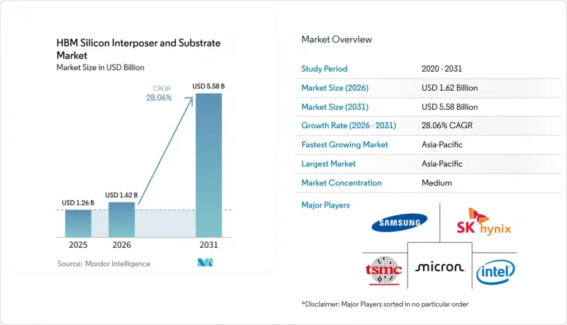
本報告按中介層類型(被動矽中介層等)、基板類型(有機構裝基板等)、封裝技術(2.5D封裝、3D封裝等)、應用(AI加速器、資料中心GPU等)、最終用戶(無晶圓半導體公司等)和地區進行細分。市場預測以美元計價。
HBM矽中介層和基板市場的全球趨勢和洞察。
AI加速器中HBM產能的快速擴張
HBM產能的快速成長仍是HBM矽中介層和基板市場最強勁的需求促進因素。這是因為每個AI封裝都需要中介層產能、先進的基板支援以及嚴格認證的組裝流程,而非通用封裝。 AI加速器的日益普及使得封裝供應直接阻礙因素了出貨量。換句話說,中介層和基板供應商如今對產品上市時間的影響程度,在以往的運算週期中是前所未有的。這種轉變增強了晶圓代工廠和高階基板製造商的商業性地位,因為客戶擴大在大規模生產開始前就鎖定產能。此外,大規模AI封裝包含更多晶片、更高的佈線密度,並承受更大的熱應力,這意味著封裝製程中的缺陷可能會抵消晶圓階段所獲得的優勢。因此,HBM矽中介層和基板市場不再僅僅受記憶體普及率的驅動,而是取決於整個AI封裝生態系統在不影響良率和可靠性預期的前提下,能夠以多快的速度擴展。
將HBM整合到高效能資料中心GPU中
隨著記憶體頻寬在資料中心GPU專案中從次要因素轉變為核心效能變量,HBM矽中介層和基板市場正朝著更大的中介層尺寸、更精細的佈線和更高密度的供電結構發展。在HBM4及後續設計中,底層晶片和堆疊層的互連結構承擔著更大的功能性責任,這使得封裝級設計決策的重要性日益凸顯。此外,隨著I/O寬度的增加和微凸塊間距的縮小,佈線負載也在增加,使得中介層設計與系統效能、散熱特性和基板整合度更加緊密地連結在一起。從實際角度來看,GPU開發人員現在將中介層和基板堆疊層視為運算平臺本身的一部分,從而可以在設計週期的早期階段做出封裝決策。這種設計方法使得在專案後期更難取代先進的封裝技術,進一步提升了其在長期產品藍圖中的重要性,並推動了HBM矽中介層和基板市場的發展。
TSV流程的複雜性和漫長的認證週期
由於複雜的幾何形狀、熱應力效應以及單一製程模組中漫長的客戶認證週期等因素,矽通孔(TSV)的製造仍然是HBM矽中介層和基板市場中最明顯的技術瓶頸。隨著每一代HBM技術的推出,這項挑戰都更加嚴峻,因為禁區範圍的縮小和佈線密度的增加會減少設計裕量和工藝公差。在IEEE IRPS 2025會議上發表的研究表明,縮小TSV的禁區範圍會透過電遷移和介質擊穿降低BEOL的可靠性,這表明認證要求正在變得更加嚴格,而不是更加寬鬆。這種技術負擔正在減緩供應商的擴張速度,因為即使資金到位,客戶仍要求在新的製程流程投入量產之前進行完整的電氣、熱學和可靠性檢驗。因此,與許多相關的半導體產業相比,HBM矽中介層和基板市場面臨強勁的需求,但供應成長卻較為緩慢。
細分市場分析
到2025年,被動式矽中介層將佔該細分市場銷售額的88.21%,在所有目前量產的AI和GPU封裝中,為HBM矽中介層和基板市場奠定堅實的基礎。這一主導地位源自於多年累積的製程技術、成熟的TSV整合技術以及與2.5D封裝流程的兼容性,而2.5D封裝流程已被領先的加速器專案廣泛採用。被動式設計還具有更簡單的價值提案,無需增加增加製程複雜性或認證工作的邏輯功能,即可實現高密度佈線和HBM整合。這種性能與可製造性的平衡使得被動式中介層即使在系統要求不斷提高的情況下,仍能保持其在封裝設計中的核心地位。
然而,這一領域仍在經歷結構性轉型。這是因為,在新一代HBM中,大部分控制、電源管理和訊號處理功能都轉移到了基片和記憶體堆疊層下方的層。因此,主動和嵌入式方法變得越來越重要,尤其是在那些要求運算晶片、HBM堆疊和支援邏輯之間更緊密整合的專案中,封裝的作用遠不止於簡單的訊號佈線。預計到2031年,嵌入式矽中介層的複合年成長率將達到28.67%,這表明HBM的矽中介層和基板市場正在為將佈線密度與額外功能控制相結合的架構鋪平道路。 《微系統與奈米工程研究》雜誌的研究表明,TSV佈局決策可以再形成晶片級應力模式,隨著中介層從被動佈線平面向功能整合度更高的設計轉變,這一點將變得越來越重要。也就是說,向嵌入式邏輯的轉變正在加速藍圖的變化,其速度超過了現有製造基礎設施的變化,因此被動式設計很可能在預測期內的大部分時間仍將是大規模生產的核心。
到2025年,基於黏合劑鍵合配方(ABF)的有機構裝基板將佔據該細分市場92.33%的佔有率,在當前加速器、GPU和HPC封裝結構的HBM矽中介層和基板市場中佔據核心地位。 ABF持續佔據主導地位的原因在於其對多層結構、精細重分佈以及將大型矽結構與高密度封裝佈線相結合所需的機械平衡的支持。此外,該細分市場還受益於一個強大的現有生態系統,領先供應商已累積了關於翹曲控制、良率穩定性和大尺寸尺寸堆疊設計的製程技術。憑藉這一現有基礎,即使客戶已經在考慮下一代替代方案,ABF仍然是大多數現有項目的首選。
供應商的投資趨勢進一步印證了這個觀點,其主要的產能擴張計畫仍瞄準高性能積體電路基板,而非迅速從ABF平台轉型。 Ibiden已宣布一項5,000億日圓(約33億美元)的投資計劃,用於2026年至2028年間高性能積體電路構裝基板的研發,併計劃於2027年開始量產。同時,玻璃構裝基板預計將以28.85%的複合年成長率成長至2031年,因為它們能夠提高超大封裝的尺寸穩定性並降低介電損耗。玻璃在HBM矽中介層和基板市場最具吸引力,因為該市場需要突破傳統回縮和翹曲的限制,實現面板式尺寸縮放。然而,玻璃的商業性化應用取決於供應商能否在生產規模上控制脆性、通孔形成和製程一致性。因此,儘管ABF仍將是核心收入來源,但對於要求最苛刻的封裝形式而言,玻璃仍將是重要的選擇。
區域分析
預計到2025年,亞太地區將佔HBM矽中介層和基板市場82.78%的銷售額,並在2031年之前以28.14%的複合年成長率持續成長,鞏固其在該市場的核心地位。這一主導地位源於關鍵供應鏈流程在台灣、韓國、日本以及東南亞快速成長地區的集中,從而縮短了晶圓代工廠、記憶體製造商、基板供應商和組裝合作夥伴之間的反饋週期。台灣憑藉其在先進封裝領域的卓越領導地位和客戶認可度,保持著其核心地位;韓國則為HBM記憶體生產及相關封裝需求奠定了基礎。日本憑藉其在基板材料和高性能構裝基板的技術實力,展現出強大的市場影響力,並持續鞏固該地區在尖端封裝結構領域的領先地位。儘管這種集中性賦予了亞太地區規模和速度優勢,但也意味著HBM矽中介層和基板市場仍然極易受到區域內局部地產能限制和供應商瓶頸的影響。
北美在HBM矽中介層和基板市場佔據第二大佔有率。這是因為許多最重要的AI加速器、GPU和客製化ASIC專案都在北美製定,即使製造工作在亞太地區進行。該地區的優勢在於其架構主導、以客戶為中心的理念以及長期的平台藍圖,這些路線圖塑造了跨多個產品世代的封裝堆疊所需的性能。因此,即使實體封裝在其他地方製造,北美的需求也會影響中介層的尺寸、基板的複雜性和認證優先順序。正因如此,儘管目前北美的製造佔有率較小,但它在HBM矽中介層和基板市場仍然保持著強大的商業性地位。
歐洲在HBM矽中介層和基板市場仍保持著較為謹慎的態度,但憑藉其基板技術、工程能力以及與客戶合作的擴張計劃,依然保持著重要的戰略地位。在AMD和英特爾等客戶的長期承諾支持下,AT&S於2026年6月宣佈在克林姆(Klim)追加高達20億歐元(23.2億美元)的投資。由於與中介層和高階基板相關的先進半導體製造能力有限,南美洲、中東和非洲在HBM矽中介層和基板市場中的佔有率仍然較小。東南亞作為商業中心的重要性日益凸顯,美光科技在新加坡推動封裝和晶圓製造,並擴大其廣泛的產能,鞏固了其在該地區封裝領域的地位。
其他好處:
- Excel格式的市場預測(ME)表
- 3個月的分析師支持
目錄
第1章:引言
- 研究假設和市場定義
- 調查範圍
第2章:調查方法
第3章執行摘要
第4章 市場狀況
- 市場概覽
- 市場促進因素
- AI加速器中HBM產能的快速擴張
- 先進封裝技術中採用共封裝記憶體和晶片組
- 高層中介層製造中良率最佳化的壓力
- 將HBM整合到高效能資料中心GPU中
- 亞太地區先進包裝在地化計劃
- 下一代HBM堆疊混合鍵結的製備現狀
- 市場限制因素
- TSV流程的複雜性和漫長的認證週期
- 中介層晶圓供應短缺及設備瓶頸
- 大封裝中因過熱導致的翹曲和次品晶片良率降低。
- 擴大先進基板和中介層的產能需要大量資本投資。
- 產業價值鏈分析
- 監理情勢
- 技術展望
- 波特五力分析
- 宏觀經濟因素對市場的影響
第5章 市場規模與成長預測
- 中介型
- 無源矽中介層
- 有源矽中介層
- 嵌入式矽中介層
- 依基材類型
- 有機構裝基板
- 玻璃構裝基板
- 矽橋/矽載體
- 其他基質類型
- 產品技術
- 2.5D包裝
- 3D包裝
- 晶片包裝
- 混合鍵合
- 透過使用
- 人工智慧加速器
- 用於資料中心的GPU
- 高效能運算
- 用於網路和交換器的專用積體電路
- 汽車人工智慧平台
- 家用電子產品
- 最終用戶
- 垂直整合設備製造商(IDM)
- 無晶圓廠半導體公司
- OSAT
- 鑄造廠
- 按地區
- 北美洲
- 美國
- 加拿大
- 墨西哥
- 歐洲
- 德國
- 英國
- 法國
- 義大利
- 其他歐洲國家
- 亞太地區
- 中國
- 日本
- 韓國
- 台灣
- 印度
- 其他亞太國家
- 南美洲
- 中東和非洲
- 北美洲
第6章 競爭情勢
- 市場集中度
- 策略趨勢
- 市佔率分析
- 公司簡介
- Taiwan Semiconductor Manufacturing Company Limited
- Samsung Electronics Co., Ltd.
- Intel Corporation
- ASE Technology Holding Co., Ltd.
- Amkor Technology, Inc.
- SK hynix Inc.
- Micron Technology, Inc.
- Fujitsu Limited
- Unimicron Technology Corp.
- Ibiden Co., Ltd.
- Shinko Electric Industries Co., Ltd.
- Kinsus Interconnect Technology Corp.
- LG Innotek Co., Ltd.
- Daeduck Electronics Co., Ltd.
- AT&S Austria Technologie und Systemtechnik AG
- Toppan Inc.
- Powertech Technology Inc.
- United Microelectronics Corporation
第7章 市場機會與未來展望
According to Mordor Intelligence, the HBM silicon interposer and substrate market size is expected to increase from USD 1.26 billion in 2025 to USD 1.62 billion in 2026 and reach USD 5.58 billion by 2031, growing at a CAGR of 28.06% over 2026-2031.
This report is Segmented by Interposer Type (Passive Silicon Interposer, and More), Substrate Type (Organic Package Substrate, and More), Packaging Technology (2. 5D Packaging, 3D Packaging, and More), Application (AI Accelerators, Data Center GPUs, and More), End User (Fabless Semiconductor Companies, and More), and Geography. The Market Forecasts are Provided in Terms of Value (USD).
Global HBM Silicon Interposer and Substrate Market Trends and Insights
Rapid HBM Capacity Expansion in AI Accelerators
Rapid HBM output growth remains the strongest demand trigger for the HBM silicon interposer and substrate market, because each AI package requires interposer capacity, advanced substrate support, and tightly qualified assembly flows rather than commodity packaging. The rise in AI accelerator deployments has made packaging availability a direct limiter on shipments, meaning interposer and substrate vendors now influence product timing in ways they did not in earlier compute cycles. This shift has strengthened the commercial position of foundries and high-end substrate makers, since customers increasingly reserve capacity well before volume production begins. It has also raised the value of process consistency, because large AI packages carry more die, more routing density, and higher thermal stress, so a weak packaging step can erase gains made at the wafer stage. As a result, the HBM silicon interposer and substrate market is no longer driven only by memory adoption, but by the speed at which the full AI package ecosystem can scale without breaking yield or reliability expectations.
HBM Integration in High-Performance Data Center GPUs
Data center GPU programs are driving the HBM silicon interposer and substrate market toward larger interposer footprints, finer routing, and denser power-delivery structures, as memory bandwidth is now a core performance variable rather than a supporting feature. HBM4 and later designs place greater functional weight on the base die and the interconnect fabric beneath the stack, increasing the importance of package-level engineering decisions. The routing burden also rises as I/O width expands and microbump pitch tightens, so interposer design becomes more closely tied to system performance, thermal behavior, and board-level integration. In practical terms, GPU developers now treat the interposer and substrate stack as part of the compute platform itself, which brings packaging decisions forward in the design cycle. That design behavior supports the HBM silicon interposer and substrate market by making advanced packaging harder to substitute late in a program and more central to long-term product roadmaps.
TSV Process Complexity and Long Qualification Cycles
TSV fabrication remains the clearest technical restraint on the HBM silicon interposer and substrate market, as it combines fine geometry, thermal stress exposure, and long customer qualification cycles into a single process block. The challenge grows with each HBM generation, as tighter keep-out zones and denser routing reduce the available space for design margin and process error. Research presented at IEEE IRPS 2025 showed that shrinking TSV keep-out zones can weaken BEOL reliability through electromigration and dielectric breakdown, indicating that qualification is becoming more demanding rather than easier. That technical burden slows supplier expansion, because even when capital is available, customers still require full electrical, thermal, and reliability validation before new flows enter production. The result is that the HBM silicon interposer and substrate market can show strong demand while still facing slower supply than in many adjacent semiconductor segments.
Other drivers and restraints analyzed in the detailed report include:
- Co-Packaged Memory and Chiplet Adoption in Advanced Packaging
- Yield Optimization Pressure in High-Layer Count Interposer Builds
- Interposer Wafer Supply Tightness and Tool Bottlenecks
For complete list of drivers and restraints, kindly check the Table Of Contents.
Segment Analysis
Passive silicon interposers accounted for 88.21% of segment revenue in 2025, making them the clear foundation of the HBM silicon interposer and substrate market across current high-volume AI and GPU packages. Their lead reflects long process learning, mature TSV integration, and compatibility with 2.5D packaging flows that already serve leading accelerator programs at scale. Passive designs also benefit from a simpler value proposition, because they deliver dense routing and HBM integration without adding logic functions that would increase process complexity and qualification work. That balance between performance and manufacturability kept passive interposers at the center of package design even as system requirements continued to rise.
The same segment still faces a structural transition, because newer HBM generations shift more control, power management, and signal handling toward the base die and the layers immediately below the memory stack. Active and embedded approaches, therefore, gain relevance when the package must do more than just route signals, especially in programs that seek tighter integration among compute dies, HBM stacks, and supporting logic. Embedded silicon interposers are projected to expand at a 28.67% CAGR through 2031, signaling that the HBM silicon interposer and substrate market is opening the door to architectures that combine routing density with added functional control. Research in Microsystems and Nanoengineering showed that TSV layout decisions can reshape die-level stress patterns, which becomes more important when interposers move from passive routing planes toward more functionally integrated designs. Even so, passive designs are likely to remain the volume anchor for much of the forecast period, because the shift toward embedded logic changes the roadmap faster than it changes the installed manufacturing base.
Organic package substrates based on ABF held 92.33% of the segment in 2025, which placed them at the center of the HBM silicon interposer and substrate market for current accelerator, GPU, and HPC package structures. ABF remains dominant because it supports high layer counts, fine redistribution, and the mechanical balance needed to pair large silicon structures with dense package routing. The segment also benefits from a strong incumbent ecosystem, where leading suppliers have already built process know-how around warpage control, yield stability, and large-format build-up designs. That installed base makes ABF the default choice for most current programs, even when customers are already studying next-generation alternatives.
Supplier investment patterns reinforce that position, since major capacity programs continue to target high-performance IC substrates rather than a sudden platform shift away from ABF. Ibiden announced a JPY 500 billion (USD 3.3 billion) investment program for high-performance IC package substrates across fiscal year 2026 to fiscal year 2028, with mass production set to begin from fiscal year 2027. At the same time, glass package substrates are projected to grow at a 28.85% CAGR through 2031, because they offer a path toward better dimensional stability and lower dielectric loss in very large packages. The appeal of glass is strongest where the HBM silicon interposer and substrate market needs panel-style scaling beyond conventional reticle and warpage limits, yet commercial uptake will depend on whether suppliers can manage brittleness, via formation, and process consistency at production scale. For that reason, ABF remains the core revenue base while glass continues to define an important future option for the most demanding package formats.
Complete Report Scope:
- By Interposer Type
- Passive Silicon Interposer
- Active Silicon Interposer
- Embedded Silicon Interposer
- By Substrate Type
- Organic Package Substrate
- Glass Package Substrate
- Silicon Bridge/Silicon Carrier
- Other Substrate Types
- By Packaging Technology
- 2.5D Packaging
- 3D Packaging
- Chiplet Packaging
- Hybrid Bonding
- By Application
- AI Accelerators
- Data Center GPUs
- High Performance Computing
- Networking and Switch ASICs
- Automotive AI Platforms
- Consumer Electronics
- By End User
- Integrated Device Manufacturers (IDMs)
- Fabless Semiconductor Companies
- OSATs
- Foundries
- By Geography
- North America
- United States
- Canada
- Mexico
- Europe
- Germany
- United Kingdom
- France
- Italy
- Rest of Europe
- Asia-Pacific
- China
- Japan
- South Korea
- Taiwan
- India
- Rest of Asia-Pacific
- South America
- Middle East and Africa
- North America
Geography Analysis
Asia-Pacific accounted for 82.78% of revenue in 2025 and is projected to expand at a 28.14% CAGR through 2031, keeping it firmly at the center of the HBM silicon interposer and substrate market. The region leads because the most critical supply chain steps are clustered across Taiwan, South Korea, Japan, and growing parts of Southeast Asia, which shortens feedback loops between foundries, memory makers, substrate suppliers, and assembly partners. Taiwan remains central through its advanced packaging leadership and deep customer qualification, while South Korea anchors HBM memory production and related packaging demand. Japan adds significant weight through its substrate materials and high-performance package substrate capabilities, which continue to support the region's leadership in leading-edge package construction. This concentration gives Asia-Pacific scale and speed, but it also means the HBM silicon interposer and substrate market remains highly exposed to localized capacity constraints and supplier bottlenecks within the region.
North America holds the second-largest position in the HBM silicon interposer and substrate market because many of the most important AI accelerator, GPU, and custom ASIC programs are defined there even when manufacturing remains in Asia-Pacific. The region's strength lies in architecture ownership, customer concentration, and long-term platform roadmaps that shape what the packaging stack must deliver over multiple product generations. North American demand therefore influences interposer size, substrate complexity, and qualification priorities even when the physical package is built elsewhere. This keeps the region commercially powerful in the HBM silicon interposer and substrate market despite its smaller current manufacturing share.
Europe remains more selective in the HBM silicon interposer and substrate market, but it retains strategic relevance through substrate technology, engineering capability, and customer-linked expansion programs. AT&S announced up to EUR 2 billion (USD 2.32 billion), in additional expansion at Kulim in June 2026, backed by long-term customer commitments from AMD and Intel. South America and the Middle East and Africa still represent a small share of the HBM silicon interposer and substrate market because they have limited advanced semiconductor manufacturing tied to interposers and high-end substrates. Southeast Asia is becoming more important as an operating base, with Micron advancing packaging and wafer fabrication in Singapore and broader capacity buildouts improving the region's place in the packaging map.
- Taiwan Semiconductor Manufacturing Company Limited
- Samsung Electronics Co., Ltd.
- Intel Corporation
- ASE Technology Holding Co., Ltd.
- Amkor Technology, Inc.
- SK hynix Inc.
- Micron Technology, Inc.
- Fujitsu Limited
- Unimicron Technology Corp.
- Ibiden Co., Ltd.
- Shinko Electric Industries Co., Ltd.
- Kinsus Interconnect Technology Corp.
- LG Innotek Co., Ltd.
- Daeduck Electronics Co., Ltd.
- AT&S Austria Technologie und Systemtechnik AG
- Toppan Inc.
- Powertech Technology Inc.
- United Microelectronics Corporation
Additional Benefits:
- The market estimate (ME) sheet in Excel format
- 3 months of analyst support
TABLE OF CONTENTS
1 INTRODUCTION
- 1.1 Study Assumptions and Market Definition
- 1.2 Scope of the Study
2 RESEARCH METHODOLOGY
3 EXECUTIVE SUMMARY
4 MARKET LANDSCAPE
- 4.1 Market Overview
- 4.2 Market Drivers
- 4.2.1 Rapid HBM Capacity Expansion in AI Accelerators
- 4.2.2 Co-Packaged Memory and Chiplet Adoption in Advanced Packaging
- 4.2.3 Yield Optimization Pressure In High-Layer Count Interposer Builds
- 4.2.4 HBM Integration in High-Performance Data Center GPUs
- 4.2.5 Advanced Packaging Localization Programs in Asia-Pacific
- 4.2.6 Hybrid Bonding Readiness for Next-Generation HBM Stacks
- 4.3 Market Restraints
- 4.3.1 TSV Process Complexity and Long Qualification Cycles
- 4.3.2 Interposer Wafer Supply Tightness and Tool Bottlenecks
- 4.3.3 Thermal Warpage and Known-Good-Die Yield Loss in Large Packages
- 4.3.4 High Capex for Advanced Substrate And Interposer Capacity
- 4.4 Industry Value Chain Analysis
- 4.5 Regulatory Landscape
- 4.6 Technological Outlook
- 4.7 Porter's Five Forces Analysis
- 4.7.1 Bargaining Power of Suppliers
- 4.7.2 Bargaining Power of Buyers
- 4.7.3 Threat of New Entrants
- 4.7.4 Threat of Substitutes
- 4.7.5 Intensity of Competitive Rivalry
- 4.8 Impact of Macroeconomic Factors on the Market
5 MARKET SIZE AND GROWTH FORECASTS (VALUE)
- 5.1 By Interposer Type
- 5.1.1 Passive Silicon Interposer
- 5.1.2 Active Silicon Interposer
- 5.1.3 Embedded Silicon Interposer
- 5.2 By Substrate Type
- 5.2.1 Organic Package Substrate
- 5.2.2 Glass Package Substrate
- 5.2.3 Silicon Bridge/Silicon Carrier
- 5.2.4 Other Substrate Types
- 5.3 By Packaging Technology
- 5.3.1 2.5D Packaging
- 5.3.2 3D Packaging
- 5.3.3 Chiplet Packaging
- 5.3.4 Hybrid Bonding
- 5.4 By Application
- 5.4.1 AI Accelerators
- 5.4.2 Data Center GPUs
- 5.4.3 High Performance Computing
- 5.4.4 Networking and Switch ASICs
- 5.4.5 Automotive AI Platforms
- 5.4.6 Consumer Electronics
- 5.5 By End User
- 5.5.1 Integrated Device Manufacturers (IDMs)
- 5.5.2 Fabless Semiconductor Companies
- 5.5.3 OSATs
- 5.5.4 Foundries
- 5.6 By Geography
- 5.6.1 North America
- 5.6.1.1 United States
- 5.6.1.2 Canada
- 5.6.1.3 Mexico
- 5.6.2 Europe
- 5.6.2.1 Germany
- 5.6.2.2 United Kingdom
- 5.6.2.3 France
- 5.6.2.4 Italy
- 5.6.2.5 Rest of Europe
- 5.6.3 Asia-Pacific
- 5.6.3.1 China
- 5.6.3.2 Japan
- 5.6.3.3 South Korea
- 5.6.3.4 Taiwan
- 5.6.3.5 India
- 5.6.3.6 Rest of Asia-Pacific
- 5.6.4 South America
- 5.6.5 Middle East and Africa
- 5.6.1 North America
6 COMPETITIVE LANDSCAPE
- 6.1 Market Concentration
- 6.2 Strategic Moves
- 6.3 Market Share Analysis
- 6.4 Company Profiles (includes Global Level Overview, Market Level Overview, Core Segments, Financials as available, Strategic Information, Market Rank/Share, Products and Services, Recent Developments)
- 6.4.1 Taiwan Semiconductor Manufacturing Company Limited
- 6.4.2 Samsung Electronics Co., Ltd.
- 6.4.3 Intel Corporation
- 6.4.4 ASE Technology Holding Co., Ltd.
- 6.4.5 Amkor Technology, Inc.
- 6.4.6 SK hynix Inc.
- 6.4.7 Micron Technology, Inc.
- 6.4.8 Fujitsu Limited
- 6.4.9 Unimicron Technology Corp.
- 6.4.10 Ibiden Co., Ltd.
- 6.4.11 Shinko Electric Industries Co., Ltd.
- 6.4.12 Kinsus Interconnect Technology Corp.
- 6.4.13 LG Innotek Co., Ltd.
- 6.4.14 Daeduck Electronics Co., Ltd.
- 6.4.15 AT&S Austria Technologie und Systemtechnik AG
- 6.4.16 Toppan Inc.
- 6.4.17 Powertech Technology Inc.
- 6.4.18 United Microelectronics Corporation
7 MARKET OPPORTUNITIES AND FUTURE OUTLOOK
- 7.1 White-Space and Unmet-Need Assessment

 快速入口裝卸鎖門市場規模、佔有率及成長分析:依機構/驅動系統、真空壓力耐受等級、結構材料/基材、最終用途產業及地區分類-2026-2033年產業預測
 中介層和矽橋市場報告:趨勢、預測和競爭分析(至2035年)
 GPU晶圓需求:市佔率分析、產業趨勢與統計、成長預測(2026-2031年)GPU程式設計平台:市佔率分析、產業趨勢與統計、成長預測(2026-2031年)
 中介層及矽橋市場規模、佔有率、成長、全球產業分析、區域趨勢及2026年至2034年預測GPU和HPC用矽中介層:市場佔有率分析、產業趨勢與統計數據以及成長預測(2026-2031年)
 2026年全球量子模擬器市場報告2026年全球多模態記憶體市場報告2026 年 AI 工作負載的 RoCE(基於融合乙太網路的 RDMA)全球市場報告
 伺服器和高效能運算用ABF基板市場:按應用、材料類型、層數和基板厚度分類,全球預測,2026-2032年