


 |
市場調查報告書
商品編碼
2099425
GPU晶圓需求:市佔率分析、產業趨勢與統計、成長預測(2026-2031年)GPU Wafer Demand - Market Share Analysis, Industry Trends & Statistics, Growth Forecasts (2026 - 2031) |
||||||

※ 本網頁內容可能與最新版本有所差異。詳細情況請與我們聯繫。
據 Mordor Intelligence 稱,GPU 晶圓需求市場預計將從 2025 年的 8,400 萬美元成長到 2026 年的 1.12 億美元,到 2031 年達到 2.85 億美元,2026 年至 2031 年的複合年成長率為 20.54%。
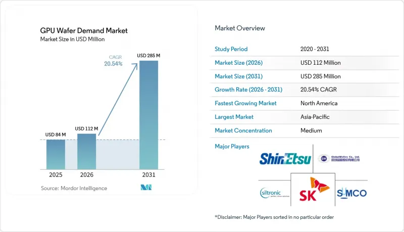
本報告按晶圓直徑(300 毫米晶圓和 200 毫米及以下晶圓)、原料晶圓類型(優質拋光體矽晶圓、外延矽晶圓、SOI 等)、製程節點(2 奈米及以下、3 奈米、4 奈米至 5 奈米及其他)、GPU 應用程式(2 奈米及以下、3 奈米、4 奈米至 5 奈米及其他)、GPU 應用程式(2 奈米及以下)以及獨立資料中心和其他地區進行細分、獨立資料中心和其他地區進行階段。市場預測以美元 (USD) 為單位。
全球GPU晶圓需求市場趨勢及洞察
隨著人工智慧訓練整合技術的進步,對缺陷極少的晶圓的需求也不斷成長。
GPU晶圓需求市場正受到人工智慧訓練日益成長的實體負載的驅動。這是因為,即使是表面品質和缺陷控制方面的微小偏差,在大規模運算晶片上也是接受度的。因此,即使在先進節點上良率略有下降,也會導致生產價值的顯著損失,使得晶圓品質成為晶圓代工廠和GPU供應商直接面臨的成本問題。據信越化學公司稱,在截至2026年3月的會計年度中,用於GPU和高頻寬記憶體的AI晶片佔300mm晶圓總需求的略低於10%,而包括資料中心和伺服器在內的更廣泛的AI相關終端市場則佔300mm晶圓總需求的20%以上。隨著這一構成比的增加,能夠持續供應極其平整且缺陷極少的基板的供應商將獲得更強的定價權,並在高級認證項目中佔據更有利的地位。因此,在GPU晶圓需求市場中,能夠與晶圓代工廠在缺陷預算和製程控制方面密切合作的晶圓製造商將更受青睞。這是因為這種合作關係很可能在多個節點升級過程中持續存在。
3nm和2nm GPU量產規模的擴大將提振優質晶圓的需求。
隨著主流GPU專案向更精細的製程節點邁進,對基板效能和生產計畫的要求也越來越高,GPU晶圓需求市場也不斷擴大。這項轉變意義重大,因為節點升級不僅能提升晶片效能,還能提高每條經認證的晶圓生產線在最先進邏輯晶片上開工生產的商業性價值。 SUMCO報告稱,2025年300毫米晶圓出貨量將成長9%。這主要得益於人工智慧領域對先進邏輯晶片和高頻寬記憶體的需求,也標誌著市場從週期早期的低迷中明顯復甦。 SUMCO也表示,預計未來3-4年內,用於人工智慧應用的DRAM晶圓需求將從目前的每月50萬至60萬片成長到每月150萬片。這顯示人工智慧運算的成長與上游矽晶片需求密切相關。在 GPU 晶圓需求市場,這個節點過渡增加了對高品質 300 毫米材料的需求,縮小了無法跟上大規模先進生產推出的低規格供應商的生存空間。
高純度多晶矽的供應限制了 300 毫米晶圓的產量。
由於電子級多晶矽供應緊張,GPU晶圓市場需求面臨嚴峻挑戰。這是因為先進晶圓生產依賴純度極高的原料,而這些原料難以被低純度材料取代。 2025年8月,美國半導體產業協會(SIA)向美國商務部報告稱,其對關鍵矽原料和晶圓產品的進口依賴仍然是國內半導體產業擴張的戰略弱點。美國地質調查局(USGS)也證實,儘管到2025年美國仍有三家公司生產多晶矽,但第四家公司由於未能滿足客戶的品質和數量標準而停產,這降低了國內產柔軟性,而先進節點的需求卻持續成長。這種緊張局面對GPU晶圓市場需求產生了重大影響,因為除了晶圓廠產能之外,原料品質也可能成為瓶頸,阻礙晶圓產能的平穩擴張。在新的認證供應商達到商業規模之前,高品質的300mm基板可能仍將受到堅挺的價格和有限供應的支撐。
細分市場分析
截至2025年,300毫米晶圓將佔據GPU晶圓市場需求的97.11%,預計2026年至2031年間,該細分市場將以21.21%的複合年成長率成長。如此巨大的市場佔有率不僅反映了技術因素,也反映了經濟因素。隨著晶片複雜性、製程精度和產出價值的不斷提升,小尺寸晶圓難以有效率地擴大先進GPU的生產規模。因此,GPU晶圓市場需求將繼續圍繞300毫米平台展開,而小於200毫米的晶圓將主要用於基於老一代製程節點的傳統遊戲、嵌入式和邊緣運算產品。這種分類是結構性的,而非暫時性的,因為小尺寸晶圓與尖端AI加速器(目前以及未來將在很大程度上決定採購決策)的相關性有限。從實際角度來看,GPU晶圓市場需求已經形成了一種層級式的尺寸結構,其中300毫米晶圓幾乎佔據了所有先進價值的創造。
此外,300mm晶圓市場對價格有顯著影響,因為幾乎所有先進邏輯晶片的主要供應瓶頸都源自於已認證的300mm生產線及其相關的材料生態系統。對這種規格晶圓的需求集中,支撐著長期合約、穩健的產能擴張以及已獲得高階客戶認可的供應商的議價能力。因此,GPU晶圓需求市場更依賴300mm晶圓的運轉率、認證狀態和區域產能分佈,而非晶圓總數本身。小直徑晶圓在一些細分領域和成本敏感型專案中仍然很重要,但它們在GPU晶圓需求市場中並不構成相同的收入基礎。正因如此,主要供應商的新投資公告仍專注於提升先進的300mm晶圓產能,而不是全面擴張所有直徑規格的晶圓。
預計到2025年,優質拋光體矽晶圓將佔據82.33%的市場佔有率,而外延矽晶圓預計將在2026年至2031年間以21.62%的複合年成長率成長。優質拋光基板仍是目前GPU生產的主要基礎,能夠滿足現有4nm-7nm製程專案的需求,而無需完全過渡到更高級的工程化原料。然而,隨著先進設計對電氣性能和製程控制的要求日益嚴格,GPU晶圓需求市場正逐漸向更均衡的配置轉變,外延晶圓和其他特殊晶圓也將佔據一部分。這種轉變不僅在晶圓產量方面意義重大,而且在提升材料專業知識的價值方面也至關重要。此外,這也提高了供應商的競爭門檻,因為他們需要對污染、電阻率和均勻性進行更嚴格的控制,才能參與下一代認證。
儘管最小基板晶圓的市場佔有率仍然有限,但隨著人工智慧系統越來越依賴對專用材料堆疊和光連接模組的支持,其戰略地位正在日益凸顯。根據Soytec預測,2026會計年度邊緣和雲端人工智慧相關銷售額將達到2.14億歐元(2.25億美元),其中光電SOI銷售額突破1億美元的速度超出預期。這顯示工程矽在人工智慧基礎設施投資中的重要性日益增加。在GPU晶圓需求市場,這意味著儘管最大的細分市場仍然是高品質拋光體矽,但成長的主導力正在轉向支援下一代架構和封裝需求的基板。因此,GPU晶圓需求產業正變得更加主導規格,基板晶圓的選擇越來越依賴系統級設計要求,而非傳統的大量生產實務。這一發展趨勢為外延晶圓在整個預測期內實現高階成長提供了清晰的路徑。
區域分析
預計到2025年,亞太地區仍將佔據GPU晶圓需求市場86.44%的佔有率,市場主要集中在台灣、韓國和日本。這反映出先進GPU製造仍以台灣為中心,韓國支撐著主要的記憶體和晶圓代工廠代工產能,而日本則承擔了大部分上游晶圓供應。日本的信越半導體和SUMCO合計佔據了全球300mm矽晶圓供應量的60%以上,憑藉其靠近主要製造群的優勢,亞太地區擁有強大的材料優勢。 SUMCO在2026年第一季的展望中也證實,儘管對非先進產品和200mm規格晶圓的需求依然疲軟,但對用於人工智慧資料中心的先進邏輯和DRAM晶圓的需求預計將保持強勁。信越半導體進一步表示,目前人工智慧相關晶圓的整體需求佔 300 毫米晶圓總需求的 20% 以上,並且預計 2026 年 4 月至 6 月的成長將超過最初的預測,這凸顯了該地區在本輪週期中的主導地位。
預計2026年至2031年間,北美地區的GPU晶圓需求將以21.42%的複合年成長率成長,成為成長最快的地區。主要驅動力是政策支援的本地化,因為聯邦政府的獎勵與美國半導體和人工智慧基礎設施的擴張相契合。美國商務部向GlobalWafers提供的津貼將支持美國20多年來首個先進的300毫米高產能矽晶圓製造平台,進一步推動該地區在地化基板在地採購。 NVIDIA承諾到2026年與台積電、富士康和康寧等合作夥伴共同在美國建設高達5000億美元的人工智慧基礎設施,這強烈表明市場對加強國內供應鏈的需求。然而,客戶認證、晶圓代工廠排產以及本地材料產量的調整仍需時間,才能在北美GPU晶圓需求市場充分發揮其優勢。
儘管歐洲在GPU晶圓生產總量中所佔佔有率較小,但憑藉其專業的供應商能力和對300毫米製程擴張的資金支持,仍發揮重要作用。 2026年6月,Siltronic公司籌集了2.73億歐元(約2.98億美元),以支持其300毫米晶圓的長期成長策略,顯示市場對先進矽晶圓的需求持續充滿信心。 Soytec公司也鞏固了其在歐洲高價值細分市場的地位,該公司報告稱,其2026會計年度光電SOI晶片的銷售額超過1億美元。這進一步凸顯了該地區在人工智慧系統中光學和工程矽的作用。 2026年,南美洲、中東和非洲在GPU晶圓需求市場中仍處於邊緣地位,這些地區的業務活動更集中在下游電子產業和未來國家主導的人工智慧相關支出上,而非上游晶圓製造。因此,全部區域的整體情況仍然清晰。這是因為亞太地區在規模上仍然處於主導地位,北美正處於最快的成長軌道上,而歐洲則繼續在特種材料和先進材料領域保持其關鍵地位。
其他好處:
- Excel格式的市場預測(ME)表
- 3個月的分析師支持
目錄
第1章:引言
- 研究假設和市場定義
- 調查範圍
第2章:調查方法
第3章執行摘要
第4章 市場狀況
- 市場概覽
- 市場促進因素
- 人工智慧訓練密度的不斷提高,推動了對缺陷極少的晶圓的需求。
- 隨著 3 奈米和 2 奈米 GPU 的量產不斷推進,對優質晶圓的需求也不斷成長。
- 背面供電導致對外延技術規格提出了更嚴格的要求。
- 在地化獎勵正在重塑晶圓的策略採購。
- 基於晶片組的GPU架構正在推動對SOI和特殊晶圓的需求。
- 永續發展計畫正在加速研發領域採用回收晶圓;
- 市場限制因素
- 高純度多晶矽供不應求限制了 300 毫米晶圓的生產。
- GPU客戶認證週期的延長導致更換供應商的進程延遲。
- 對Float-Zone和優質晶圓的資本投資提高了進入門檻。
- 中國對先進節點設備的出口限制正在減緩其業務擴張速度。
- 產業價值鏈分析
- 宏觀經濟因素對市場的影響
- 監理情勢
- 技術展望
- 波特五力分析
- 價格分析
第5章 市場規模與成長預測
- 依晶圓直徑
- 300毫米晶圓
- 200毫米或更小
- 依晶片類型
- 優質拋光塊狀矽晶片
- 外延矽晶片
- SOI 和其他工程矽晶片
- 按行程節點
- 2奈米或更小
- 3 nm
- 4 nm~5 nm
- 6 nm~7 nm
- 8 nm~16 nm
- 16奈米或更大
- GPU 應用
- 用於資料中心和人工智慧/高效能運算的GPU
- 用於遊戲和消費用途的獨立顯示卡
- 專業視覺化與工作站 GPU
- 汽車、嵌入式和邊緣 GPU
- 按地區
- 北美洲
- 美國
- 加拿大
- 墨西哥
- 歐洲
- 德國
- 英國
- 法國
- 義大利
- 其他歐洲國家
- 亞太地區
- 中國
- 日本
- 韓國
- 印度
- 東南亞
- 其他亞太國家
- 南美洲
- 中東和非洲
- 北美洲
第6章 競爭情勢
- 市場集中度
- 策略趨勢
- 市佔率分析
- 公司簡介
- Shin-Etsu Handotai Co., Ltd.
- SUMCO Corporation
- Siltronic AG
- GlobalWafers Co., Ltd.
- SK Siltron Co., Ltd.
- Soitec SA
- Wafer Works Corporation
- Shanghai Simgui Technology Co., Ltd.
- Okmetic Oyj
- Ferrotec Holdings Corporation
- Hangzhou Silicon Tech Co., Ltd.
- Zhonghuan Semiconductor Co., Ltd.
- POSCO Future M Co., Ltd.
- Episil-Precision Inc.
- MEMC Korea Company
- Korea Silicon Wafer Co., Ltd.
- Linton Crystal Technologies
- Salem Advanced Materials Inc.
- Noel Technologies
- Topsil GlobalWafers
第7章 市場機會與未來展望
According to Mordor Intelligence, the GPU wafer demand market size is expected to increase from USD 84.00 million in 2025 to USD 112.00 million in 2026 and reach USD 285.00 million by 2031, growing at a CAGR of 20.54% over 2026-2031.
This report is Segmented by Wafer Diameter (300 Mm Wafers and 200 Mm and Below), Starting Wafer Type (Prime Polished Bulk Silicon Wafers, Epitaxial Silicon Wafers, and SOI and More), Process Node (2 Nm and Below, 3 Nm, 4 Nm To 5 Nm, and More), GPU Application (Data Center and AI/HPC GPUs, Gaming and Consumer Discrete GPUs, and More), and Geography. The Market Forecasts are Provided in Terms of Value (USD).
Global GPU Wafer Demand Market Trends and Insights
AI Training Density Raises Ultra-Low Defect Wafer Requirements
The GPU wafer demand market is being pushed higher by the physical intensity of AI training, because very large compute die are less tolerant of even small variations in surface quality and defect control. That makes wafer quality a direct cost issue for foundries and GPU vendors, since small yield losses at advanced nodes can erase large amounts of output value. Shin-Etsu said AI chips for GPUs and high-bandwidth memory accounted for just under 10% of total 300 mm wafer demand, while broader AI-related end markets, including data centers and servers, exceeded 20% of total 300 mm demand in the fiscal year ended March 2026. As that mix rises, suppliers that can consistently deliver ultra-flat and low-defect substrates gain stronger pricing power and a more protected position inside advanced qualification programs. The GPU wafer demand market therefore rewards wafer makers that can work closely with foundries on defect budgets and process control, because those relationships are likely to carry forward across multiple node transitions.
3 nm and 2 nm GPU Ramps Increase Prime Wafer Pull
The GPU wafer demand market is also rising as leading GPU programs move into smaller process nodes that require more exacting substrate performance and tighter production planning. This shift matters not only because node migration improves chip capability, but also because it raises the commercial value of each qualified wafer start inside advanced logic lines. SUMCO reported that 300 mm wafer shipments grew 9% in 2025, led by leading-edge logic and high-bandwidth memory demand tied to AI, which marked a clear recovery from the weaker conditions seen earlier in the cycle. SUMCO also said AI-use DRAM wafer demand is expected to rise from 500,000-600,000 wafers per month currently to 1,500,000 wafers per month over the next 3-4 years, which shows how tightly AI compute growth is now linked to upstream silicon requirements. In the GPU wafer demand market, that node migration strengthens demand for prime 300 mm material and narrows the room for lower-specification suppliers that cannot serve advanced production ramps at scale.
High-Purity Polysilicon Supply Limits 300 mm Output
The GPU wafer demand market faces a real supply restraint from electronic-grade polysilicon, because advanced wafer production depends on very high purity feedstock that is not easily replaced by lower-grade material. The Semiconductor Industry Association told the US Department of Commerce in August 2025 that import dependence across key silicon inputs and wafer products remains a strategic weakness for domestic semiconductor expansion. USGS also confirmed that 3 companies produced polysilicon in the United States in 2025, while a 4th ceased production after failing to meet customer quality and volume standards, which reduced domestic flexibility at the same time that advanced-node demand kept rising. That tightness matters for the GPU wafer demand market because wafer capacity cannot expand smoothly when feedstock quality, rather than only fab equipment, becomes the limiting step. Until new qualified supply reaches commercial scale, premium 300 mm substrates are likely to remain supported by a firm pricing floor and limited availability.
Other drivers and restraints analyzed in the detailed report include:
- Backside Power Delivery Increases Epitaxial Specification Intensity
- Localization Incentives Re-Shape Strategic Wafer Procurement
- Long GPU Customer Qualification Cycles Delay Supplier Switching
For complete list of drivers and restraints, kindly check the Table Of Contents.
Segment Analysis
300 mm wafers held 97.11% of GPU wafer demand market share in 2025, and the segment is projected to grow at a 21.21% CAGR from 2026 to 2031. That dominance reflects economics as much as technology, because advanced GPU production simply cannot be scaled efficiently on smaller formats once die complexity, process precision, and output value all move higher. The GPU wafer demand market therefore remains centered on the 300 mm platform, while 200 mm and below mostly serve legacy gaming, embedded, and edge products built on older nodes. This split is structural rather than temporary, since the smaller-diameter category has limited relevance for the leading AI accelerators that now shape most forward purchasing decisions. In practical terms, the GPU wafer demand industry has already settled around a format hierarchy where 300 mm captures nearly all advanced value creation.
The 300 mm segment also has an outsized influence on pricing, because nearly every major supply bottleneck in advanced logic now runs through qualified 300 mm lines and their associated materials ecosystem. Demand concentration in that format supports long contract periods, disciplined capacity additions, and stronger bargaining power for suppliers that already hold advanced customer approvals. The GPU wafer demand market is therefore more exposed to 300 mm utilization, qualification status, and regional capacity location than to total wafer unit counts alone. Smaller diameters still matter for some niche and cost-sensitive programs, but they do not shape the revenue base of the GPU wafer demand market in the same way. This is why new investment announcements from leading suppliers continue to target advanced 300 mm output rather than broad-based expansion across all diameter classes.
Prime polished bulk silicon wafers held 82.33% share of 2025 demand, while epitaxial silicon wafers are projected to expand at a 21.62% CAGR from 2026 to 2031. Prime polished substrates remain the working base for large volumes of current GPU production because they fit the needs of established 4 nm to 7 nm programs without requiring a full shift toward more engineered starting material. Even so, the GPU wafer demand market is gradually moving toward a richer mix of epitaxial and other engineered wafers as tighter electrical performance and process control requirements spread across advanced designs. This shift matters because it raises the value of materials expertise, not only the value of raw wafer volume. It also raises the competitive threshold for suppliers, since they need stronger control over contamination, resistivity, and uniformity to participate in next-wave qualifications.
The smallest starting wafer categories remain limited in share, but their strategic role is rising as AI systems place more value on specialty material stacks and optical interconnect support. Soitec said Edge and Cloud AI revenue reached EUR 214 million, or USD 225 million, in fiscal year 2026, and Photonics-SOI revenue exceeded USD 100 million earlier than expected, which shows that engineered silicon has become more important inside AI infrastructure spending. In the GPU wafer demand market, this means the largest segment still rests with prime polished bulk silicon, but growth leadership is shifting toward substrates that help support next-generation architecture and packaging needs. The GPU wafer demand industry is therefore becoming more specification-led, with starting wafer choice increasingly linked to system-level design requirements rather than to legacy volume habits. That progression gives epitaxial wafers a clearer path to premium growth through the forecast period.
Complete Report Scope:
- By Wafer Diameter
- 300 mm Wafers
- 200 mm and Below
- By Starting Wafer Type
- Prime Polished Bulk Silicon Wafers
- Epitaxial Silicon Wafers
- SOI and Other Engineered Silicon Wafers
- By Process Node
- 2 nm and Below
- 3 nm
- 4 nm to 5 nm
- 6 nm to 7 nm
- 8 nm to 16 nm
- Above 16 nm
- By GPU Application
- Data Center and AI/HPC GPUs
- Gaming and Consumer Discrete GPUs
- Professional Visualization and Workstation GPUs
- Automotive, Embedded, and Edge GPUs
- By Geography
- North America
- United States
- Canada
- Mexico
- Europe
- Germany
- United Kingdom
- France
- Italy
- Rest of Europe
- Asia-Pacific
- China
- Japan
- South Korea
- India
- Southeast Asia
- Rest of Asia-Pacific
- South America
- Middle East and Africa
- North America
Geography Analysis
Asia-Pacific retained 86.44% of GPU wafer demand market share in 2025, which keeps the regional base of the GPU wafer demand market heavily concentrated around Taiwan, South Korea, and Japan. This position reflects the fact that advanced GPU fabrication remains centered in Taiwan, while South Korea supports key memory and foundry capacity and Japan anchors a large share of upstream wafer supply. Japan's Shin-Etsu Handotai and SUMCO together hold over 60% of global 300 mm silicon wafer supply, which gives the region a strong materials advantage close to leading fabrication clusters. SUMCO's first-quarter 2026 guidance also confirmed continued strength in advanced logic and DRAM wafers for AI data centers, even as non-advanced products and 200 mm formats remained softer. Shin-Etsu further said broader AI-related wafer demand exceeded 20% of total 300 mm demand and that growth from April to June 2026 was expected to outpace earlier projections, which supports the region's lead in the current cycle.
North America is projected to grow at a 21.42% CAGR from 2026 to 2031, making it the fastest-rising geography in the GPU wafer demand market. The main driver is policy-backed localization, because federal incentives are now aligned with domestic semiconductor and AI infrastructure expansion. The US Department of Commerce award to GlobalWafers supports the first advanced high-volume 300 mm silicon wafer manufacturing platform in the United States in more than 20 years, which gives the region a clearer path toward local substrate availability. NVIDIA's 2026 commitment to build up to USD 500 billion of AI infrastructure in the United States with partners including TSMC, Foxconn, and Corning adds a strong demand-side signal for domestic supply chain development. Even so, the GPU wafer demand market in North America will still need time to align customer qualification, foundry schedules, and local materials output before the full benefit appears.
Europe holds a smaller direct position in volume, but it remains relevant through specialized supplier capabilities and balance-sheet support for 300 mm expansion. Siltronic raised EUR 273 million, or USD 298 million, in June 2026 to support its long-term 300 mm growth strategy, which points to continued confidence in advanced silicon demand. Soitec also strengthened Europe's position in high-value niches by reporting Photonics-SOI revenue above USD 100 million in fiscal year 2026, which ties the region more closely to optical and engineered silicon roles in AI systems. South America and the Middle East and Africa remain peripheral to the GPU wafer demand market in 2026, with activity focused more on downstream electronics and future sovereign AI spending than on upstream wafer manufacturing. The overall regional picture therefore remains clear, because Asia-Pacific still leads in scale, North America is building the fastest new growth path, and Europe is defending a focused position in specialty and advanced materials.
- Shin-Etsu Handotai Co., Ltd.
- SUMCO Corporation
- Siltronic AG
- GlobalWafers Co., Ltd.
- SK Siltron Co., Ltd.
- Soitec S.A.
- Wafer Works Corporation
- Shanghai Simgui Technology Co., Ltd.
- Okmetic Oyj
- Ferrotec Holdings Corporation
- Hangzhou Silicon Tech Co., Ltd.
- Zhonghuan Semiconductor Co., Ltd.
- POSCO Future M Co., Ltd.
- Episil-Precision Inc.
- MEMC Korea Company
- Korea Silicon Wafer Co., Ltd.
- Linton Crystal Technologies
- Salem Advanced Materials Inc.
- Noel Technologies
- Topsil GlobalWafers
Additional Benefits:
- The market estimate (ME) sheet in Excel format
- 3 months of analyst support
TABLE OF CONTENTS
1 INTRODUCTION
- 1.1 Study Assumptions and Market Definition
- 1.2 Scope of the Study
2 RESEARCH METHODOLOGY
3 EXECUTIVE SUMMARY
4 MARKET LANDSCAPE
- 4.1 Market Overview
- 4.2 Market Drivers
- 4.2.1 AI Training Density is Raising Ultra-Low Defect Wafer Requirements
- 4.2.2 3 Nanometer and 2 Nanometer GPU Ramps are Increasing Prime Wafer Pull
- 4.2.3 Backside Power Delivery is Increasing Epitaxial Specification Intensity
- 4.2.4 Localization Incentives are Re-Shaping Strategic Wafer Procurement
- 4.2.5 Chiplet-Based GPU Architectures are Expanding SOI and Specialty Wafer Demand
- 4.2.6 Sustainability Programs are Accelerating Reclaimed Wafer Adoption in R&D
- 4.3 Market Restraints
- 4.3.1 High-Purity Polysilicon Supply is Limiting 300 Millimeter Output
- 4.3.2 Long GPU Customer Qualification Cycles Are Delaying Supplier Switching
- 4.3.3 Float-Zone and Prime Wafer Capex is Raising Entry Barriers
- 4.3.4 Export Controls on Advanced Node Equipment are Slowing China Expansion
- 4.4 Industry Value Chain Analysis
- 4.5 Impact of Macroeconomic Factors on the Market
- 4.6 Regulatory Landscape
- 4.7 Technological Outlook
- 4.8 Porter's Five Forces Analysis
- 4.8.1 Bargaining Power of Suppliers
- 4.8.2 Bargaining Power of Buyers
- 4.8.3 Threat of New Entrants
- 4.8.4 Threat of Substitutes
- 4.8.5 Intensity of Competitive Rivalry
- 4.9 Pricing Analysis
5 MARKET SIZE AND GROWTH FORECASTS (VALUE)
- 5.1 By Wafer Diameter
- 5.1.1 300 mm Wafers
- 5.1.2 200 mm and Below
- 5.2 By Starting Wafer Type
- 5.2.1 Prime Polished Bulk Silicon Wafers
- 5.2.2 Epitaxial Silicon Wafers
- 5.2.3 SOI and Other Engineered Silicon Wafers
- 5.3 By Process Node
- 5.3.1 2 nm and Below
- 5.3.2 3 nm
- 5.3.3 4 nm to 5 nm
- 5.3.4 6 nm to 7 nm
- 5.3.5 8 nm to 16 nm
- 5.3.6 Above 16 nm
- 5.4 By GPU Application
- 5.4.1 Data Center and AI/HPC GPUs
- 5.4.2 Gaming and Consumer Discrete GPUs
- 5.4.3 Professional Visualization and Workstation GPUs
- 5.4.4 Automotive, Embedded, and Edge GPUs
- 5.5 By Geography
- 5.5.1 North America
- 5.5.1.1 United States
- 5.5.1.2 Canada
- 5.5.1.3 Mexico
- 5.5.2 Europe
- 5.5.2.1 Germany
- 5.5.2.2 United Kingdom
- 5.5.2.3 France
- 5.5.2.4 Italy
- 5.5.2.5 Rest of Europe
- 5.5.3 Asia-Pacific
- 5.5.3.1 China
- 5.5.3.2 Japan
- 5.5.3.3 South Korea
- 5.5.3.4 India
- 5.5.3.5 Southeast Asia
- 5.5.3.6 Rest of Asia-Pacific
- 5.5.4 South America
- 5.5.5 Middle East and Africa
- 5.5.1 North America
6 COMPETITIVE LANDSCAPE
- 6.1 Market Concentration
- 6.2 Strategic Moves
- 6.3 Market Share Analysis
- 6.4 Company Profiles (includes Global Level Overview, Market Level Overview, Core Segments, Financials as available, Strategic Information, Market Rank/Share, Products and Services, Recent Developments)
- 6.4.1 Shin-Etsu Handotai Co., Ltd.
- 6.4.2 SUMCO Corporation
- 6.4.3 Siltronic AG
- 6.4.4 GlobalWafers Co., Ltd.
- 6.4.5 SK Siltron Co., Ltd.
- 6.4.6 Soitec S.A.
- 6.4.7 Wafer Works Corporation
- 6.4.8 Shanghai Simgui Technology Co., Ltd.
- 6.4.9 Okmetic Oyj
- 6.4.10 Ferrotec Holdings Corporation
- 6.4.11 Hangzhou Silicon Tech Co., Ltd.
- 6.4.12 Zhonghuan Semiconductor Co., Ltd.
- 6.4.13 POSCO Future M Co., Ltd.
- 6.4.14 Episil-Precision Inc.
- 6.4.15 MEMC Korea Company
- 6.4.16 Korea Silicon Wafer Co., Ltd.
- 6.4.17 Linton Crystal Technologies
- 6.4.18 Salem Advanced Materials Inc.
- 6.4.19 Noel Technologies
- 6.4.20 Topsil GlobalWafers
7 MARKET OPPORTUNITIES AND FUTURE OUTLOOK
- 7.1 White-Space and Unmet-Need Assessment

 快速入口裝卸鎖門市場規模、佔有率及成長分析:依機構/驅動系統、真空壓力耐受等級、結構材料/基材、最終用途產業及地區分類-2026-2033年產業預測
 中介層和矽橋市場報告:趨勢、預測和競爭分析(至2035年)
 用於 HBM 的矽中介層和基板:市場佔有率分析、行業趨勢和統計數據以及成長預測(2026-2031 年)GPU程式設計平台:市佔率分析、產業趨勢與統計、成長預測(2026-2031年)
 中介層及矽橋市場規模、佔有率、成長、全球產業分析、區域趨勢及2026年至2034年預測GPU和HPC用矽中介層:市場佔有率分析、產業趨勢與統計數據以及成長預測(2026-2031年)
 2026年全球量子模擬器市場報告2026年全球多模態記憶體市場報告2026 年 AI 工作負載的 RoCE(基於融合乙太網路的 RDMA)全球市場報告
 伺服器和高效能運算用ABF基板市場:按應用、材料類型、層數和基板厚度分類,全球預測,2026-2032年