


 |
市場調查報告書
商品編碼
2099411
用於DRAM的矽晶圓:市場佔有率分析、行業趨勢和統計數據以及成長預測(2026-2031年)DRAM Silicon Wafer - Market Share Analysis, Industry Trends & Statistics, Growth Forecasts (2026 - 2031) |
||||||

※ 本網頁內容可能與最新版本有所差異。詳細情況請與我們聯繫。
根據 Mordor Intelligence 預測,DRAM 中使用的矽晶圓市場規模預計將在 2025 年達到 21.5 億美元,2026 年達到 24.1 億美元,到 2031 年達到 33.4 億美元,2026 年至 2031 年的複合成長率 6.74%。
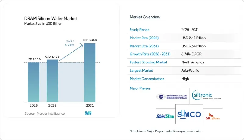
本報告以晶圓直徑(300毫米[12吋]、200毫米[8吋]和小於150毫米[6吋或更小])、晶圓型式(拋光晶圓和外延[epi]晶圓)、DRAM型態(標準DRAM、行動DRAM[LPDDR]、圖形DRAM[GDDR]、DRAM型態(標準DRAM、行動DRAM[LPDDR]、圖形DRAM[GDDR]、DRAM和另一個地區的區域市場預測以美元(USD)計價。
全球DRAM矽晶圓市場趨勢及洞察
對HBM和先進DRAM節點的需求不斷成長
DRAM矽晶圓市場正受到HBM和先進DRAM節點需求成長的推動。這些產品需要更嚴格的製程控制、更均勻的原料,以及透過更長的生產過程來確保高品質300mm拋光晶圓的可靠供應。根據SEMI的報告,2025年全球矽晶圓出貨量將達到12973微平方英吋(MSI),成長5.8%。推動此復甦的關鍵因素包括對HBM相關拋光晶圓的需求以及對邏輯晶片相關先進外延晶圓的需求。這種產品組合對基板供應商意義重大,因為先進記憶體專案佔用了更大比例的認證產能,減少了分配給標準DRAM生產線的靈活產能空間。韓國《中央日報》2026年5月的一篇報道稱,鑑於需求沒有放緩的跡象,三星已加快了其位於平澤的P6晶片工廠的建設。這證實了先進記憶體專案的需求將繼續推動整個區域供應鏈的發展。在 DRAM 矽晶圓市場,認證晶圓的供應仍然是一個重要的阻礙因素,因此客戶的興趣仍然集中在及時交付高品質基板,而不是僅僅關注運作中的晶圓廠的數量。
擴展人工智慧和資料中心的內存
DRAM矽晶圓市場也受惠於人工智慧資料中心的擴張。這推動了對HBM產品和高容量伺服器記憶體的需求,並增加了整個供應鏈中部署的晶圓密集型記憶體專案數量。 SEMI預計,到2026年,前端設備投資將達到1,330億美元,光是記憶體設備投資就將成長13%,顯示大量資金正湧入先進半導體產能。這種投資模式意義重大,因為它表明人工智慧基礎設施不僅推動了單一系列記憶體產品的發展,而且還強化了涵蓋晶圓需求、設備需求和認證活動的更廣泛的投資週期。據半導體產業協會(SIA)稱,美國半導體公司每年採購價值135億美元的矽晶圓,預計到2029年這一數字將達到183億美元。這凸顯了基板供應在未來半導體生產中日益重要的經濟意義。在DRAM矽晶圓市場,人工智慧伺服器的日益普及為訂單前景帶來了更清晰的指引,從標準拋光晶圓到更高檔次的基板,訂單量均有所成長。這是因為記憶體採購不再局限於單一裝置類型,而是涵蓋了廣泛的應用領域。
300毫米晶圓擴容的資本密集度
用於DRAM的矽晶圓市場仍面臨供應緊張的局面。這是因為擴大300毫米晶圓產能成本高昂,生產系統需要數年時間才能推出,並且在新生產線完全產生收入和現金流之前,會給供應商帶來沉重的折舊免稅額負擔。據Siltronic公司稱,其位於新加坡的一座新的300毫米晶圓廠在2025年增加了3.43億歐元(3.88億美元)的折舊免稅額費用,導致全年息稅前利潤為負2600萬歐元(2900萬美元),儘管銷售額持平。這顯示新晶圓產能的投資回收期非常長。 SUMCO公司也累計,其在2026年第一季的營運虧損為53億歐元(3,400萬美元),並解釋說,虧損的主要原因是過去資本投資的折舊免稅額費用增加,而不是終端需求的急劇下降。因此,供應商將不得不承擔數年的成本,直到新的產能具備商業性可行性,這導致新投資緩解出貨量、價格和客戶合約分配緊張狀況的速度放緩。在DRAM矽晶圓市場,資本密集度是一個直接的阻礙因素,因為它限制了供應的快速響應,即使訂單前景良好且買家願意簽訂長期合約也是如此。
細分市場分析
到2025年,300mm晶圓將佔據DRAM矽晶圓市場86.43%的佔有率,成為整個供應鏈中需求、投資計畫和客戶認證活動的核心。這項主導地位源自於先進DRAM單元需要精確的微影術、嚴格的良率控制和成熟的製程基礎設施,而這些只有在採用最先進製程節點的300mm晶圓規模下才能實現商業化生產的經濟可行性。 SUMCO指出,2025年對300mm晶圓的需求成長了9%,並表示先進DRAM應用的這一成長動能將持續到2026年。這印證了最大直徑規格在當前客戶專案中日益重要的觀點。根據 SEMI 的報告,2026 年第一季全球矽晶圓出貨量將達到 3,275 MSI,年增 13.1%,先進記憶體和邏輯元件將推動復甦,這與將推動 300 毫米基板消耗的需求趨勢密切相關。
由於小直徑晶圓目前仍局限於小眾和傳統應用領域,因此它們對先進DRAM專案構不成大規模挑戰,也不會實質地改變DRAM矽晶圓市場的主要商業性價值來源。據Siltronic公司稱,到2026年初,除人工智慧相關應用外,客戶庫存水準仍將居高不下,這表明非先進晶圓的需求疲軟,並凸顯了先進晶圓和傳統晶圓之間日益擴大的經濟差距。該公司還宣布,其生產150毫米及以下晶圓的SD生產線已於2025年關閉,這證實了隨著供應商調整產品組合以轉向更相關的基板類型,傳統直徑晶圓的產能正在逐步淘汰,而非升級。在DRAM矽晶圓市場,晶圓直徑如今已成為節點世代的明確指標,300毫米晶圓代表先進DRAM,而較小尺寸的晶圓則處於該類別的邊緣,很少吸引戰略投資。
區域分析
預計到2025年,亞太地區將佔據DRAM矽晶圓市場78.64%的佔有率,繼續保持其在該領域的中心地位,並成為連接基板供應和先進記憶體製造的重要通道。韓國是該地區的核心,三星電子和SK海力士為全球先進DRAM和HBM生產中心提供支援。透過多年期客戶計劃,韓國在確保認證矽晶圓的供應方面發揮著至關重要的作用。根據《韓國中央日報》報道,三星平澤P5工廠和正在快速建設中的P6工廠預計月產量將達到60萬片,這表明該地區對記憶體相關矽晶圓的需求將進一步顯著成長。日本也在加強類似的供應管道。信越半導體和SUMCO兩家公司合計供應全球超過一半的300毫米矽晶圓,該地區高度相互依存,日本的矽晶圓生產與韓國的記憶體生產緊密相連。
預計到2031年,北美地區將以8.18%的複合年成長率成長,成為DRAM矽晶圓市場成長最快的地區。同時,北美也是供應鏈在地化從政策層面轉化為實際產能的最典型案例。這項轉變得益於《晶片法案》(CHIPS Act)對本地晶圓供應的支持,而在此投資週期開始之前,美國在先進的300毫米商用規模上很少見到這種支持。據美國國家標準與技術研究院(NIST)稱,GlobalWafers America和MEMC LLC已獲得高達4.06億美元的直接資金,用於支持在德克薩斯州和密蘇裡州的40億美元晶圓投資。這將為該地區的本土基板採購奠定更堅實的基礎。位於德克薩斯州謝爾曼的計畫定位為美國首個先進的大批量300毫米矽晶圓工廠。其意義在於,它將使記憶體和邏輯晶片客戶更便捷地取得本地原料。美國半導體產業協會 (SIA) 預測,到 2029 年,美國矽晶圓採購額將達到 183 億美元,這也解釋了為什麼國內買家正在尋求更廣泛、更強大的供應基礎。
歐洲雖然在技術深度方面仍然扮演著重要角色,但其關注點更多地放在特種晶圓生產和工藝研發上,而非新建待開發區生產項目,因此在短期內擴大DRAM矽晶圓市場佔有率方面,歐洲的地位並不像其他地區那樣舉足輕重。 Siltronic表示,其新加坡工廠將於2025年8月進入折舊免稅額期,並且其2026年的銷售額將面臨外匯波動、SD生產線關閉以及除AI相關市場以外的其他地區庫存調整帶來的壓力。這表明,歐洲供應商仍在努力平衡新興業務的成長與傳統業務的疲軟。中國也尋求深化區域自主化,根據《日經亞洲》報道,中國已設定政策目標,要求國內半導體製造商到2026年底,其70%以上的矽晶圓採購來自中國供應商。即使在價格壓力下,這也將促進本土企業的擴張計畫。因此,在整個 DRAM 矽晶圓市場中,區域分佈正從單一的、以亞洲主導的生產走廊轉向更廣泛但仍然高度集中的結構,國內供應目標的成長速度超過了經認證的新產能的擴張速度。
其他好處:
- Excel格式的市場預測(ME)表
- 3個月的分析師支持
目錄
第1章:引言
- 研究假設和市場定義
- 調查範圍
第2章:調查方法
第3章執行摘要
第4章 市場狀況
- 市場概覽
- 市場促進因素
- 對HBM和下一代DRAM節點的需求不斷成長
- 人工智慧和資料中心記憶體擴展
- 記憶體積體電路基板向 300 毫米過渡
- 政府對國內晶圓供應鏈的支持措施
- 對DRAM良率和均勻性有嚴格的製程控制要求。
- 特種晶圓供應的本地化
- 市場限制因素
- 擴大300毫米晶圓生產需要大量資本投入
- 對原料和高純度多晶矽的依賴
- 認證風險和客戶核准流程所需時間
- 地緣政治重新分配導致供應鏈波動
- 產業價值鏈分析
- 監理情勢
- 技術展望
- 宏觀經濟因素對市場的影響
- 波特五力分析
第5章 市場規模與成長預測
- 依晶圓直徑
- 300毫米(12吋)
- 200毫米(8吋)
- 小於150毫米(6吋或更小)
- 依晶片類型
- 拋光晶片
- 外延(Epi)晶片
- DRAM 類型
- 標準DRAM
- 行動DRAM(LPDDR)
- 圖形顯存(GDDR)
- 伺服器DRAM
- 專用及汽車用DRAM
- 按地區
- 北美洲
- 歐洲
- 亞太地區
- 中國
- 日本
- 韓國
- 台灣
- 其他亞太國家
- 世界其他地區
第6章 競爭情勢
- 市場集中度
- 策略趨勢
- 市佔率分析
- 公司簡介
- Shin-Etsu Handotai Co., Ltd.
- SUMCO Corporation
- GlobalWafers Co., Ltd.
- Siltronic AG
- SK Siltron Co., Ltd.
- Soitec SA
- Okmetic Oyj
- Wafer Works Corporation
- RS Technologies Co., Ltd.
- Topsil Semiconductor Materials A/S
- Shanghai Simgui Technology Co., Ltd.
- National Silicon Industry Group Co., Ltd.
- GRINM Semiconductor Materials Co., Ltd.
- Zhejiang Jinruihong Technology Co., Ltd.
- Hangzhou Semiconductor Wafer Co., Ltd.
- Zhonghuan Advanced Semiconductor Materials Co., Ltd.
- FST Corporation
第7章 市場機會與未來展望
According to Mordor Intelligence, the DRAM silicon wafer market size is projected to be USD 2.15 billion in 2025, USD 2.41 billion in 2026, and reach USD 3.34 billion by 2031, growing at a CAGR of 6.74% from 2026 to 2031.
This report is Segmented by Wafer Diameter (300mm [12-Inch], 200mm [8-Inch], and Less Than 150mm [6-Inch and Below]), Wafer Type (Polished Wafers, and Epitaxial [Epi] Wafers), DRAM Type (Standard DRAM, Mobile DRAM [LPDDR], Graphics DRAM [GDDR], Server DRAM, and Specialty and Automotive DRAM), and Geography (North America, Asia-Pacific, and More). The Market Forecasts are Provided in Terms of Value (USD).
Global DRAM Silicon Wafer Market Trends and Insights
Rising Demand for HBM And Advanced DRAM Nodes
The DRAM silicon wafer market is being driven by stronger demand for HBM and advanced DRAM nodes, as these products require tighter process control, more consistent starting material, and dependable access to premium 300mm polished wafers across longer production runs. SEMI reported that global silicon wafer shipments rose 5.8% in 2025 to 12,973 MSI, with polished wafer demand linked to HBM and advanced epitaxial wafer demand linked to logic as the main volume drivers behind the recovery. That product split matters for substrate suppliers because advanced memory programs now absorb a larger share of qualified capacity, leaving less room for flexible allocation across standard DRAM lines. Korea JoongAng Daily reported in May 2026 that Samsung accelerated construction of its P6 chip plant in Pyeongtaek because demand showed no sign of easing, which reinforces the continued pull from advanced memory programs across the regional supply chain. In the DRAM silicon wafer market, this keeps customer attention fixed on the timely delivery of high-quality substrates rather than on nominal fab counts alone, because the qualified wafer pool remains the real constraint.
AI and Data Center Memory Expansion
The DRAM silicon wafer market is also benefiting from AI data center build-outs, which are lifting demand across both HBM products and large-capacity server memory, broadening the number of wafer-intensive memory programs moving through the supply chain. SEMI estimated that front-end equipment spending will reach USD 133 billion in 2026, while memory equipment spending alone will rise 13% in the same year, indicating how strongly capital is being directed toward advanced semiconductor capacity. This spending pattern matters because it shows that AI infrastructure is not pulling on only one memory product family, but instead reinforcing a larger investment cycle that spans wafer demand, tool demand, and qualification activity. The Semiconductor Industry Association stated that US chip companies purchase USD 13.5 billion in silicon wafers annually, and that this figure is expected to reach USD 18.3 billion by 2029, highlighting the growing economic weight of substrate availability for future semiconductor output. In the DRAM silicon wafer market, broader AI server deployment supports stronger order visibility across both standard polished wafers and more advanced substrate grades, as memory procurement is broadening rather than narrowing to a single device type.
Capital Intensity of 300mm Wafer Expansion
The DRAM silicon wafer market still faces a hard supply ceiling because 300mm expansion is expensive, takes years to ramp, and burdens suppliers with heavy depreciation before new lines contribute fully to earnings or cash generation. Siltronic said its new 300mm fab in Singapore added EUR 343 million (USD 388 million) to 2025 depreciation, pushing full-year EBIT to EUR -26 million (USD -29 million) even though revenue stayed flat, showing how long the payback cycle can be for new wafer capacity. SUMCO also reported a JPY 5.3 billion (USD 34 million) operating loss in Q1 2026, equivalent to, and tied that pressure mainly to higher depreciation from earlier capital spending rather than to a collapse in end demand. Suppliers therefore absorb years of costs before new output becomes commercially efficient, which slows the pace at which new investment can ease tightness in customer shipments, pricing, and contract allocation. For the DRAM silicon wafer market, capital intensity is a direct restraint because it limits fast supply response even when order visibility is strong, and buyers are willing to commit to longer agreements.
Other drivers and restraints analyzed in the detailed report include:
- 300mm Migration for Memory-Intensive Substrates
- Government Incentives for Domestic Wafer Supply Chains
- Feedstock and High-Purity Polysilicon Dependency
For complete list of drivers and restraints, kindly check the Table Of Contents.
Segment Analysis
The 300mm segment held 86.43% of the DRAM silicon wafer market share in 2025, making it the clear center of demand, investment planning, and customer qualification activity across the supply chain. It leads because advanced DRAM cells require tight lithography, strong yield control, and a mature process infrastructure, which are only economical at the 300mm scale for commercial production at leading nodes. SUMCO said 300mm wafer demand grew 9% in 2025 and pointed to continued momentum in advanced DRAM applications through 2026, which supports the view that the largest-diameter class is still gaining practical importance in current customer programs. SEMI reported that worldwide silicon wafer shipments increased 13.1% year over year in Q1 2026 to 3,275 MSI, with advanced memory and logic leading the recovery, and that aligns closely with the demand profile that favors 300mm substrate consumption.
Smaller diameters remain tied to specialty and legacy uses, so they do not compete at scale for advanced DRAM programs and do not materially alter where the main commercial value of the DRAM silicon wafer market is being created. Siltronic said customer inventories remained elevated outside AI-linked applications in early 2026, indicating weaker conditions for non-advanced wafer demand and underlining the widening gap between advanced and legacy-diameter economics. The company also closed its SD line for wafers up to 150mm in 2025, reinforcing that legacy diameter capacity is being retired rather than renewed as suppliers reshape their portfolios around more relevant substrate classes. In the DRAM silicon wafer market, wafer diameter now works as a clear proxy for node generation because 300mm aligns with advanced DRAM while smaller formats sit at the edge of the category and attract far less strategic investment.
Complete Report Scope:
- By Wafer Diameter
- 300mm (12-inch)
- 200mm (8-inch)
- Less than 150mm (6-inch and below)
- By Wafer Type
- Polished Wafers
- Epitaxial (Epi) Wafers
- By DRAM Type
- Standard DRAM
- Mobile DRAM (LPDDR)
- Graphics DRAM (GDDR)
- Server DRAM
- Specialty and Automotive DRAM
- By Geography
- North America
- Europe
- Asia-Pacific
- China
- Japan
- South Korea
- Taiwan
- Rest of Asia-Pacific
- Rest of the World
Geography Analysis
Asia-Pacific held 78.64% of the DRAM silicon wafer market share in 2025, so the region remained the clear operating center of the category and the main corridor linking substrate supply with advanced memory fabrication. South Korea sits at the core of that position because Samsung Electronics and SK Hynix anchor the global base for advanced DRAM and HBM production, giving the country an outsized role in pulling qualified wafer supply through multi-year customer programs. Korea JoongAng Daily reported that Samsung's Pyeongtaek P5 and fast-tracked P6 complex are expected to reach a combined 600,000 wafers per month, pointing to another large increase in memory-linked substrate demand from the same geography. Japan strengthens the same corridor because Shin-Etsu Handotai and SUMCO together supply more than half of the global 300mm wafer volume, linking Japanese wafer output closely with South Korean memory production and keeping the region highly interdependent.
North America is projected to grow at 8.18% CAGR through 2031, making it the fastest-growing regional slice of the DRAM silicon wafer market and the clearest example of supply localization moving from policy into physical capacity. This shift is being driven by CHIPS Act support for local wafer supply, which had been largely absent at advanced commercial 300mm scale in the United States before the current investment cycle began. NIST said GlobalWafers America and MEMC LLC received up to USD 406 million in direct funding to support USD 4 billion in Texas and Missouri wafer investments, which gives the region a stronger foundation for domestic substrate sourcing. The Sherman, Texas project is positioned as the first advanced high-volume 300mm silicon wafer plant in the United States, which matters because it brings memory and logic customers closer to local starting material supply. The Semiconductor Industry Association's projection that US silicon wafer purchases will reach USD 18.3 billion by 2029 explains why domestic buyers are pushing for a broader and more resilient supply base.
Europe remains more concentrated around specialty-grade wafer production and process research than around new greenfield scale, which keeps it relevant to technology depth but less central to near-term capacity share gains in the DRAM silicon wafer market. Siltronic said its Singapore fab entered depreciation in August 2025 and that 2026 revenue would face pressure from exchange rates, the SD line closure, and inventory corrections outside the strongest AI-linked markets, which shows that European-linked suppliers are still balancing advanced growth with weaker legacy exposure. China is also trying to deepen regional self-sufficiency, with Nikkei Asia reporting a policy target for domestic chipmakers to source more than 70% of their silicon wafers from Chinese suppliers by the end of 2026, which supports local expansion plans even under pricing pressure. Across the DRAM silicon wafer market, geography is therefore shifting from a single Asia-led production corridor toward a broader but still highly concentrated map where domestic supply goals are rising faster than qualified new capacity.
- Shin-Etsu Handotai Co., Ltd.
- SUMCO Corporation
- GlobalWafers Co., Ltd.
- Siltronic AG
- SK Siltron Co., Ltd.
- Soitec S.A.
- Okmetic Oyj
- Wafer Works Corporation
- RS Technologies Co., Ltd.
- Topsil Semiconductor Materials A/S
- Shanghai Simgui Technology Co., Ltd.
- National Silicon Industry Group Co., Ltd.
- GRINM Semiconductor Materials Co., Ltd.
- Zhejiang Jinruihong Technology Co., Ltd.
- Hangzhou Semiconductor Wafer Co., Ltd.
- Zhonghuan Advanced Semiconductor Materials Co., Ltd.
- FST Corporation
Additional Benefits:
- The market estimate (ME) sheet in Excel format
- 3 months of analyst support
TABLE OF CONTENTS
1 INTRODUCTION
- 1.1 Study Assumptions and Market Definition
- 1.2 Scope of the Study
2 RESEARCH METHODOLOGY
3 EXECUTIVE SUMMARY
4 MARKET LANDSCAPE
- 4.1 Market Overview
- 4.2 Market Drivers
- 4.2.1 Rising Demand for HBM and Advanced DRAM Nodes
- 4.2.2 AI and Data Center Memory Expansion
- 4.2.3 300mm Migration for Memory-Intensive Substrates
- 4.2.4 Government Incentives for Domestic Wafer Supply Chains
- 4.2.5 Tight Process Control Requirements for DRAM Yield and Uniformity
- 4.2.6 Supply Localization in Specialty Wafer Flows
- 4.3 Market Restraints
- 4.3.1 Capital Intensity of 300mm Wafer Expansion
- 4.3.2 Feedstock and High-Purity Polysilicon Dependency
- 4.3.3 Qualification Risk and Long Customer Approval Cycles
- 4.3.4 Supply Chain Volatility From Geopolitical Reallocation
- 4.4 Industry Value Chain Analysis
- 4.5 Regulatory Landscape
- 4.6 Technological Outlook
- 4.7 Impact of Macroeconomic Factors on the Market
- 4.8 Porter's Five Forces Analysis
- 4.8.1 Threat of New Entrants
- 4.8.2 Bargaining Power of Buyers
- 4.8.3 Bargaining Power of Suppliers
- 4.8.4 Threat of Substitutes
- 4.8.5 Industry Rivalry
5 MARKET SIZE AND GROWTH FORECASTS (VALUE)
- 5.1 By Wafer Diameter
- 5.1.1 300mm (12-inch)
- 5.1.2 200mm (8-inch)
- 5.1.3 Less than 150mm (6-inch and below)
- 5.2 By Wafer Type
- 5.2.1 Polished Wafers
- 5.2.2 Epitaxial (Epi) Wafers
- 5.3 By DRAM Type
- 5.3.1 Standard DRAM
- 5.3.2 Mobile DRAM (LPDDR)
- 5.3.3 Graphics DRAM (GDDR)
- 5.3.4 Server DRAM
- 5.3.5 Specialty and Automotive DRAM
- 5.4 By Geography
- 5.4.1 North America
- 5.4.2 Europe
- 5.4.3 Asia-Pacific
- 5.4.3.1 China
- 5.4.3.2 Japan
- 5.4.3.3 South Korea
- 5.4.3.4 Taiwan
- 5.4.3.5 Rest of Asia-Pacific
- 5.4.4 Rest of the World
6 COMPETITIVE LANDSCAPE
- 6.1 Market Concentration
- 6.2 Strategic Moves
- 6.3 Market Share Analysis
- 6.4 Company Profiles (includes Global Level Overview, Market Level Overview, Core Segments, Financials as available, Strategic Information, Market Rank/Share, Products and Services, Recent Developments)
- 6.4.1 Shin-Etsu Handotai Co., Ltd.
- 6.4.2 SUMCO Corporation
- 6.4.3 GlobalWafers Co., Ltd.
- 6.4.4 Siltronic AG
- 6.4.5 SK Siltron Co., Ltd.
- 6.4.6 Soitec S.A.
- 6.4.7 Okmetic Oyj
- 6.4.8 Wafer Works Corporation
- 6.4.9 RS Technologies Co., Ltd.
- 6.4.10 Topsil Semiconductor Materials A/S
- 6.4.11 Shanghai Simgui Technology Co., Ltd.
- 6.4.12 National Silicon Industry Group Co., Ltd.
- 6.4.13 GRINM Semiconductor Materials Co., Ltd.
- 6.4.14 Zhejiang Jinruihong Technology Co., Ltd.
- 6.4.15 Hangzhou Semiconductor Wafer Co., Ltd.
- 6.4.16 Zhonghuan Advanced Semiconductor Materials Co., Ltd.
- 6.4.17 FST Corporation
7 MARKET OPPORTUNITIES AND FUTURE OUTLOOK
- 7.1 White-Space and Unmet-Need Assessment

 DRAM模組及組件市場-2026-2032年全球市場預測
 行動DRAM:市場佔有率分析、產業趨勢與統計、成長預測(2026-2031年)伺服器DRAM:市場佔有率分析、產業趨勢與統計、成長預測(2026-2031年)CXL連接的DRAM模組:市佔率分析、產業趨勢與統計數據、成長預測(2026-2031)
 DRAM市場預測至2034年-按類型、容量、外形規格、製程節點、應用、通路和地區分類的全球分析
 自旋傳輸矩MRAM市場機會、成長要素、產業趨勢分析及2026-2035年預測
 動態隨機存取記憶體 (DRAM) 市場規模、佔有率、趨勢和預測:按類型、技術、最終用戶和地區分類,2026-2034 年
 隨機存取記憶體(RAM)市場:按類型、產品類型和地區分類動態隨機存取記憶體(DRAM)市場:按類型、技術、架構、容量、終端用戶產業、分銷管道和應用分類-2026-2032年全球市場預測
 2026年全球動態隨機存取記憶體市場報告