

 |
市場調查報告書
商品編碼
2063673
日本LED外延片:市佔率分析、產業趨勢與統計及成長預測(2026-2031年)Japan LED Epitaxial Wafer - Market Share Analysis, Industry Trends & Statistics, Growth Forecasts (2026 - 2031) |
||||||
※ 本網頁內容可能與最新版本有所差異。詳細情況請與我們聯繫。
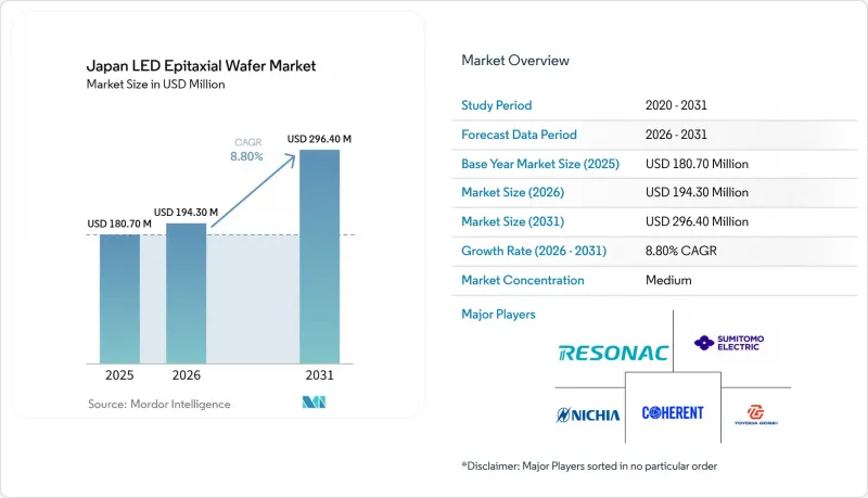
根據 Mordor Intelligence 預測,日本 LED 外延晶片市場規模將從 2025 年的 1.807 億美元成長到 2026 年的 1.943 億美元,到 2031 年將達到 2.964 億美元,2026 年至 2031 年的複合年成長率為 8.80%。
本報告按材料(GaN基外延晶片、Al-In-Ga-N基外延晶片等)、基板類型(藍寶石、矽、碳化矽(SiC)等)、晶片直徑(100mm及以下、150mm及其他)和應用(通用照明、汽車、顯示器和背光、紫外線殺菌及其他)進行細分。市場預測以美元(USD)計價。
日本LED外延晶片市場的趨勢與洞察
汽車頭燈對高亮度LED的需求日益成長
自我調整矩陣式頭燈需要平面波長變化小於1%的外延層,以防止整個光束出現色偏。日亞化學工業株式會社新成立的汽車研發中心正在加速合作開發週期,並為日本供應商提供早期設計採用機會。一級燈具製造商正透過嚴格的PPAP測試檢驗國產晶圓,並加強長期契約,以保護生產商免受商品價格波動的影響。矽基基板改善了緊湊型頭燈外殼內的溫度控管。儘管傳統照明二極體的價格有所下降,但由於每個模組的像素數量不斷增加,對晶圓的需求仍在成長。
政府對國內化合物半導體生產的獎勵
總額達1,017億日圓(約6.4億美元)的補助方案,其中包括用於提升碳化矽(SiC)外延產能的705億日圓(約4.4億美元),將降低金屬有機化學氣相沉積(MOCVD)生產線升級的資金門檻,並擴大前驅體供應基礎。共用基礎設施,例如大型氣體庫和無塵室擴建,將透過縮短氨(NH3)和三甲基鎵(TMGa)的採購前置作業時間,間接惠及LED晶圓廠。該政策的延續性體現了政府的長期承諾,並降低了私人投資下一代反應器和測量技術的風險。
對新型MOCVD反應器進行了大量資本投資。
最先進的MOCVD設備單價在150萬美元至300萬美元之間,國內工廠需要維修為多腔室配置並具備原位測量功能。在LED平均售價(ASP)持續下滑的情況下,這給企業的財務狀況帶來了壓力。日亞化學工業株式會社對閒置陰極設備的減損支出清楚地顯示了資本投資錯配帶來的風險。缺乏資金籌措管道的小規模晶圓製造商將被迫進行產業重組或退出市場。供應商的定價權進一步縮小了日本買家的議價空間。
細分市場分析
儘管AlGaN的市佔率仍然小規模,但其預期12.50%的複合年成長率反映了市場對依賴深紫外發射的消毒和感測設備日益成長的需求。日本GaN LED外延晶片市場仍然佔據主導地位,這主要得益於其在通用照明和汽車應用領域的出貨量,但創新勢頭顯然正在轉向AlGaN,後者憑藉其更長的使用壽命獲得了更高的利潤率。使用6吋藍寶石基板進行的進一步研究表明,其發光變異性僅為1.6%,證實了其大規模生產的可行性。
儘管氮化鎵(GaN)在成本和缺陷密度方面仍保持優勢,但預計未來的銷售成長將轉向鋁氮化鎵(AlGaN)和鋁銦鎵磷(AlInGaP)這一細分市場。微型LED顯示器中新型RGB顏色轉換技術的出現,導致直接髮光紅色AlInGaP的需求趨於穩定。因此,日本LED外延晶片市場可能會出現兩極化:一個是注重成本的GaN核心市場,另一個是面向長壽命紫外線應用的高利潤AlGaN前沿市場。
預計到2025年,藍寶石將佔據58.30%的市場佔有率,凸顯了其在成熟的C面製程和光學透明度方面的強勢地位。然而,矽優異的導熱性(150 W m⁻¹ K⁻¹)以及與現有CMOS生產線的兼容性,使其預期複合年成長率將達到12.80%。這項轉變將擴大矽在日本LED外延片市場的潛在市場佔有率,因為在工作溫度高於150°C的汽車頭燈模組中,GaN-on-Si設計更受青睞。
碳化矽擁有高達 490 W m⁻¹K⁻¹ 的優異散熱性能,但由於 8 吋晶圓供不應求和高成本,其廣泛應用受到限制。砷化鎵的應用仍限於特殊雷射領域。因此,藍寶石在主流 LED 市場佔據銷量主導,而矽則佔據了一個快速成長的細分市場,該市場需要散熱性能優異的垂直結構晶片。
其他好處:
- Excel格式的市場預測(ME)表
- 3個月的分析師支持
目錄
第1章:引言
- 研究假設和市場定義
- 調查範圍
第2章:調查方法
第3章執行摘要
第4章 市場狀況
- 市場概覽
- 市場促進因素
- 汽車頭燈對高亮度LED的需求日益成長。
- 政府對國內化合物半導體生產的支持措施
- MiniLED背光技術在高級電視中的快速普及
- UV-C LED在消毒設備的應用迅速成長
- 日本擴大MicroLED智慧生產線
- GaN-on-Si技術與代工廠合作的興起
- 市場限制因素
- 對新型MOCVD反應器進行大量資本投資
- 高純度氨氣供應鏈中斷
- 與低成本中國外延供應商的競爭
- 8吋碳化矽基板供不應求
- 產業供應鏈分析
- 宏觀經濟因素對市場的影響
- 監理情勢
- 技術展望
- 波特五力分析
第5章 市場規模與成長預測
- 材料
- 基於氮化鎵的外延晶片
- AlInGaP外延晶片
- AlGaN外延晶片
- 依基材類型
- 藍寶石
- 矽
- 碳化矽(SiC)
- 砷化鎵(GaAs)
- 依晶圓直徑
- 100毫米或更小
- 150 mm
- 200毫米或以上
- 透過使用
- 一般照明
- 汽車照明
- 顯示器和背光
- 紫外線消毒
- 工業和專用照明
第6章 競爭情勢
- 市場集中度
- 策略趨勢
- 市佔率分析
- 公司簡介
- Nichia Corporation
- Toyoda Gosei Co., Ltd.
- Resonac Holdings Corporation
- Sumitomo Electric Industries, Ltd.
- Shin-Etsu Chemical Co., Ltd.
- Sanan Optoelectronics Co., Ltd.
- Epistar Corporation
- Osram Opto Semiconductors GmbH
- Coherent Corp.
- SemiLEDs Corporation
- LG Innotek Co., Ltd.
- AIXTRON SE
- DOWA Electronics Materials
第7章 市場機會與未來展望
According to Mordor Intelligence, the japan lED epitaxial wafer market size is expected to increase from USD 180.7 million in 2025 to USD 194.3 million in 2026 and reach USD 296.4 million by 2031, growing at an 8.80% CAGR over 2026-2031.
This report is Segmented by Material System (GaN-Based Epitaxial Wafers, Alingap Epitaxial Wafers, and More), Substrate Type (Sapphire, Silicon, Silicon Carbide (SiC), and More), Wafer Diameter (Up To 100 Mm, 150 Mm, and More), and Application (General Lighting, Automotive, Displays and Backlighting, UV Sterilization, and More). The Market Forecasts are Provided in Terms of Value (USD).
Japan LED Epitaxial Wafer Market Trends and Insights
Intensifying Demand for High-Brightness LEDs In Automotive Headlamps
Adaptive matrix headlamps require epitaxial layers with sub-1% in-plane wavelength variation to prevent color shift across the beam. Nichia's new automotive innovation center accelerates co-development cycles, giving Japanese suppliers early design-win opportunities.Tier-1 lamp makers validate domestic wafers against stringent PPAP tests, reinforcing long contracts that shield producers from commodity price swings. Silicon substrates improve thermal management inside compact headlamp housings. The growing pixel count per module lifts wafer demand despite price compression in conventional lighting diodes.
Government Incentives for Domestic Compound-Semiconductor Production
A JPY 101.7 billion (USD 0.64 billion) subsidy package, including JPY 70.5 billion (USD 0.44 billion) directed to SiC epi capacity, lowers capital hurdles for MOCVD line upgrades and broadens the precursor supply base. Shared infrastructure, such as bulk gas farms and clean-room expansions, indirectly benefits LED wafer fabs by cutting procurement lead times for NH3 and TMGa. Policy continuity signals a long-range commitment that de-risks private investment in next-generation reactors and metrology.
High Capital Expenditure for New MOCVD Reactors
State-of-the-art MOCVD units cost USD 1.5-3 million each, and domestic plants must retrofit multi-chamber configurations with in-situ metrology, straining balance sheets just as LED ASPs decline. Nichia's impairment of idle cathode tools illustrates the risk of misaligned capex. Smaller wafer houses lacking credit access face consolidation or exit. Equipment vendors' pricing power further limits negotiation room for Japanese buyers.
Other drivers and restraints analyzed in the detailed report include:
- Rapid Penetration of MiniLED Backlighting in High-End TVs
- Surge In UV-C LED Adoption for Sterilization Equipment
- Supply Chain Disruptions for High-Purity NH3 Gas
For complete list of drivers and restraints, kindly check the Table Of Contents.
Segment Analysis
AlGaN's share remains modest, but its projected 12.50% CAGR reflects heightened demand for sterilization and sensing devices that rely on deep-UV emission. The Japan LED epitaxial wafer market size for GaN remains dominant thanks to general lighting and automotive volumes, yet innovation energy is clearly shifting toward AlGaN, where lifetime gains secure premium margins. Research breakthroughs with 6-inch sapphire templates show only 1.6% variation in emission, confirming manufacturability at scale.
GaN maintains cost and defect-density advantages, but future revenue growth tilts toward AlGaN and niche AlInGaP. Emerging RGB color-conversion paths in micro-LED displays cap direct red AlInGaP demand. Consequently, the Japan LED epitaxial wafer market will likely bifurcate into a cost-sensitive GaN core and a high-margin AlGaN frontier catering to long-life UV applications.
Sapphire's 58.30% 2025 share underscores the inertia of established C-plane recipes and optical transparency. Nevertheless, silicon's superior 150 W m-1 K-1 thermal conductivity and compatibility with existing CMOS lines underpin its projected 12.80% CAGR. Automotive headlamp modules that operate above 150 °C favor GaN-on-Si designs, a shift that enlarges silicon's addressable slice of the Japan LED epitaxial wafer market.
Silicon carbide excels in heat removal at 490 W m-1 K-1, yet 8-inch wafer scarcity and elevated cost slow adoption. Gallium arsenide remains confined to specialty lasers. Consequently, sapphire holds volume leadership in mainstream LEDs, whereas silicon captures fast-growing segments that demand thermally robust, vertically structured chips.
List of Companies Covered in this Report:
- Nichia Corporation
- Toyoda Gosei Co., Ltd.
- Resonac Holdings Corporation
- Sumitomo Electric Industries, Ltd.
- Shin-Etsu Chemical Co., Ltd.
- Sanan Optoelectronics Co., Ltd.
- Epistar Corporation
- Osram Opto Semiconductors GmbH
- Coherent Corp.
- SemiLEDs Corporation
- LG Innotek Co., Ltd.
- AIXTRON SE
- DOWA Electronics Materials
Additional Benefits:
- The market estimate (ME) sheet in Excel format
- 3 months of analyst support
TABLE OF CONTENTS
1 INTRODUCTION
- 1.1 Study Assumptions and Market Definition
- 1.2 Scope of the Study
2 RESEARCH METHODOLOGY
3 EXECUTIVE SUMMARY
4 MARKET LANDSCAPE
- 4.1 Market Overview
- 4.2 Market Drivers
- 4.2.1 Intensifying Demand for High-Brightness LEDs in Automotive Headlamps
- 4.2.2 Government Incentives for Domestic Compound-Semiconductor Production
- 4.2.3 Rapid Penetration of MiniLED Backlighting in High-End TVs
- 4.2.4 Surge in UV-C LED Adoption for Sterilization Equipment
- 4.2.5 Expansion of Smart Manufacturing Lines for MicroLED in Japan
- 4.2.6 Emergence of GaN-on-Si Technology Partnerships with Foundries
- 4.3 Market Restraints
- 4.3.1 High Capital Expenditure for New MOCVD Reactors
- 4.3.2 Supply Chain Disruptions for High-Purity Ammonia Gas
- 4.3.3 Competition from Low-Cost Chinese Epitaxy Suppliers
- 4.3.4 Limited Availability of 8-inch SiC Substrates
- 4.4 Industry Supply-Chain Analysis
- 4.5 Impact of Macroeconomic Factors on the Market
- 4.6 Regulatory Landscape
- 4.7 Technological Outlook
- 4.8 Porter's Five Forces Analysis
- 4.8.1 Threat of New Entrants
- 4.8.2 Bargaining Power of Suppliers
- 4.8.3 Bargaining Power of Buyers
- 4.8.4 Threat of Substitutes
- 4.8.5 Competitive Rivalry
5 MARKET SIZE AND GROWTH FORECASTS (VALUE)
- 5.1 By Material System
- 5.1.1 GaN-based Epitaxial Wafers
- 5.1.2 AlInGaP Epitaxial Wafers
- 5.1.3 AlGaN Epitaxial Wafers
- 5.2 By Substrate Type
- 5.2.1 Sapphire
- 5.2.2 Silicon
- 5.2.3 Silicon Carbide (SiC)
- 5.2.4 Gallium Arsenide (GaAs)
- 5.3 By Wafer Diameter
- 5.3.1 Upto 100 mm
- 5.3.2 150 mm
- 5.3.3 200 mm and Above
- 5.4 By Application
- 5.4.1 General Lighting
- 5.4.2 Automotive Lighting
- 5.4.3 Displays and Backlighting
- 5.4.4 UV Sterilization
- 5.4.5 Industrial and Specialty Lighting
6 COMPETITIVE LANDSCAPE
- 6.1 Market Concentration
- 6.2 Strategic Moves
- 6.3 Market Share Analysis
- 6.4 Company Profiles (includes Global Level Overview, Market Level Overview, Core Segments, Financials as available, Strategic Information, Market Rank/Share, Products and Services, Recent Developments)
- 6.4.1 Nichia Corporation
- 6.4.2 Toyoda Gosei Co., Ltd.
- 6.4.3 Resonac Holdings Corporation
- 6.4.4 Sumitomo Electric Industries, Ltd.
- 6.4.5 Shin-Etsu Chemical Co., Ltd.
- 6.4.6 Sanan Optoelectronics Co., Ltd.
- 6.4.7 Epistar Corporation
- 6.4.8 Osram Opto Semiconductors GmbH
- 6.4.9 Coherent Corp.
- 6.4.10 SemiLEDs Corporation
- 6.4.11 LG Innotek Co., Ltd.
- 6.4.12 AIXTRON SE
- 6.4.13 DOWA Electronics Materials
7 MARKET OPPORTUNITIES AND FUTURE OUTLOOK
- 7.1 White-Space and Unmet-Need Assessment
 碳化矽基板和外延晶片的專利趨勢調查
 AlGaN深紫外LED外延片:市佔率分析、產業趨勢與統計及成長預測(2026-2031年)藍寶石基板氮化鎵LED外延片:市佔率分析、產業趨勢與統計、成長預測(2026-2031年)
 外延晶片市場:按材料、晶片尺寸、應用和產業分類-2026-2032年全球市場預測矽外延片:市佔率分析、產業趨勢與統計、成長預測(2026-2031)
 矽外延晶片市場分析及預測(至2035年):依類型、產品、技術、應用、材料類型、裝置、製程、最終用戶及功能分類
 外延晶片市場規模、佔有率、趨勢及預測(按類型、晶片尺寸、應用、產業及地區分類),2026-2034年
 2026年全球矽外延晶片市場報告外延晶片市場-2026-2031年預測
 外延晶片市場:按類型、應用、終端用戶產業、國家及地區分類 - 全球產業分析、市場規模、市場佔有率及2025-2032年預測