


 |
市場調查報告書
商品編碼
2063439
AlGaN深紫外LED外延片:市佔率分析、產業趨勢與統計及成長預測(2026-2031年)AlGaN Deep-UV LED Epitaxial Wafer - Market Share Analysis, Industry Trends & Statistics, Growth Forecasts (2026 - 2031) |
||||||
※ 本網頁內容可能與最新版本有所差異。詳細情況請與我們聯繫。
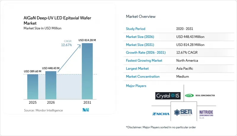
根據 Mordor Intelligence 預測,AlGaN 深紫外線 LED 外延晶片的市場規模預計將從 2025 年的 3.896 億美元和 2026 年的 4.4843 億美元成長到 2031 年的 8.1428 億美元,2026 年至 2031 年的複合年成長率為 2.67%。
本報告按基板平台(藍寶石、氮化鋁基板等)、波段(UV-A (315–400 nm)、UV-B (280–315 nm) 等)、晶圓直徑(100 mm 或以下、150 mm、200 mm 或以上)、應用領域(水和空氣消毒、表面滅菌、醫療保健設備等細分)。市場預測以美元計價。
全球AlGaN深紫外線LED外延晶片市場趨勢及洞察
監理機關禁止使用含汞紫外線燈
歐盟計劃在2025年12月前逐步淘汰含汞燈具,而RoHS指令的最終豁免將於2027年2月到期,這迫使公共產業和原始設備製造商(OEM)採用固態模組。 《水俁公約》正在加強全球標準,並確保以出口主導的亞洲製造地也面臨採用固態模組的壓力。日亞化學工業株式會社於2025年11月啟動的無汞消毒舉措,正是垂直整合供應商如何重組內部運作以符合舉措的例證。短期部署主要集中在功率低於100瓦的終端用戶系統中,因為維修成本有限,但兆瓦級市政設備的升級仍需要大量投資。因此,AlGaN深紫外線LED外延晶片的採購週期領先在住宅和攜帶式設備,之後才會擴展到工業維修。
對即用型水消毒的需求日益成長。
人們日益關注自來水和離網環境中的病原體,這推動了對配備 265–280 nm LED 的緊湊型 UV-C水質淨化器的需求。基於 AlGaN 外延晶圓的板載晶片(COB) 模組,目前可在小於 5.2 mm² 的封裝內提供 275 nm 波長下 145 mW 的功率,從而實現電池供電設計。亞太地區已發布“沸水警告”,當地居民率先採用者此類產品,災害救援機構也指定使用這種輕便的 LED 裝置進行現場部署。每個水質淨化器整合多個晶片,可實現 40 mJ/cm² 的輻照劑量,即使晶片尺寸很小,也能降低晶圓消耗。隨著產量的增加,晶圓製造商正在最佳化其 100 mm 藍寶石晶圓的加工能力,從而降低了成本門檻,對中功率領域的 AlN 模板構成挑戰。
與汞燈相比,每瓦製造成本更高。
在兆瓦規模下,UV-C LED系統的每瓦成本仍然是傳統汞燈的2到4倍,對於預算緊張的公共產業而言,投資回收期可能超過7年。由於外延晶片的成本幾乎佔裝置成本的一半,即使EQE(外量子效率)略有提高,也能直接降低組件價格。截至2024年12月,日亞化學株式會社的280nm元件的電光轉換效率為7.4%,仍主要面向高階消毒應用這一細分市場,凸顯了其與市政大規模部署之間的差距。亞太地區的電力公司面臨利潤空間緊張的困境,正在推遲大規模的裝置切換,直到晶片價格下降或獲得補貼。因此,短期內,這種限制因素在AlGaN深紫外線LED外延晶片市場最為嚴重。
細分市場分析
預計到2025年,AlGaN深紫外LED外延晶圓市場規模將達到2.3億美元,市佔率高達58.19%;而AlN基板預計將以13.28%的複合年成長率成長,到2031年貢獻超過2.6億美元的收入。藍寶石基板憑藉著成熟的供應鏈、反應器工藝和有利的價格,依然保持著市場主導地位,但其較高的位錯密度會降低深紫外線效率。相較之下,AlN的晶格匹配生長可以將缺陷密度降低到10⁶ cm⁻²以下,進而達到20-30%的穩定EQE(外量子效率)提升。 HexaTech於2026年2月推出3吋AlN晶圓,Crystal IS於2024年6月在100mm晶圓上實現了99%的有效面積,這些都顯示了AlN外延晶圓規模化發展的強勁勢頭。
這種轉變並非在不同波長上都一致。 UV-A 和 UV-B 裝置由於藍寶石鋁含量較低且抗缺陷能力強,因此仍可繼續使用藍寶石基板。但對於波長低於 270 nm 的 UV-C 裝置,採用 AlN 基板對於實現實際功率等級日益重要。隨著晶圓製造商準備生產 150mm 的 AlN 生產線,成本差距正在縮小,預計與目前的 100mm 基板相比,每晶片成本將降低 30%。如果成功,這將促使整個 AlGaN 深紫外線 LED 外延晶圓市場重新評估籌資策略,垂直整合型企業將 AlN 生長流程納入內部生產,以保護其智慧財產權和利潤率。
預計到2025年,UV-C晶片將佔銷售額的46.14%(1.8億美元),並以13.86%的複合年成長率快速成長。其265nm的殺菌峰值波長符合水、空氣和表面消毒標準。日亞化學工業株式會社(Nichia Corporation)已擴大280nm晶片的量產規模,該晶片在700mA電流下輸出功率為263mW,顯示已具備商業化條件。 UV-A主要用於固化和仿冒品檢測,其量子效率(EQE)高達35%以上,但由於燈具市場成熟,出貨量成長緩慢。 UV-B則應用於皮膚病治療和園藝領域。法規核准限制了其規模化生產,但高昂的價格彌補了銷售下滑的影響。
波長低於240奈米的遠紫外C波段(Far-UVC)仍是研發領域的前沿方向。 Silanna UV公司開發了一種波長為233奈米的裝置,其輻射強度達到2毫瓦/球面度(mW/sr),是其他裝置的兩倍,這表明其在空間消毒方面具有潛在的應用價值。然而,當鋁含量超過60%時,裝置對應變和缺陷的敏感度會增加,導致良率下降。總體而言,波長分類反映了應用需求。消毒應用推動了對UV-C的需求,而工業感測器則促進了遠紫外C波段裝置的生產,這些因素共同塑造了AlGaN深紫外線LED外延晶片市場的設計規格。
區域分析
預計到2025年,亞太地區AlGaN深紫外LED外延晶圓的銷售額將達2.2億美元,佔全球需求的55.83%。這主要歸功於垂直整合的日本和韓國供應商在基板生長、外延和裝置封裝領域的領先地位。日本製造商如日亞化學工業株式會社(Nichia Corporation)和日機裝株式會社(Nikkiso Corporation)憑藉數十年的MOCVD技術積累,而韓國企業則利用其廣泛的專利組合,與家電和水處理設備等OEM廠商簽訂長期合約。中國國內半導體策略也在投資化合物半導體生產線,但MOCVD設備和前驅體氣體的出口限制仍阻礙高性能UV-C晶圓的大規模生產。此外,該地區政府對圖案化藍寶石和氮化鋁(AlN)基板的津貼,使晶圓廠在成本上比海外競爭對手更具優勢。因此,預計亞太地區至少在2028年之前仍將是AlGaN深紫外LED外延晶圓市場的領先製造地。
在北美,預計2025年銷售額將達到9,000萬美元,並在2031年之前以12.93%的複合年成長率成長。這主要得益於《晶片創新與生產法案》(CHIPS Act)為新建氮化鋁基板工廠、反應器設施和後端封裝生產線提供的資金支援。醫療和航太產業的國內買家正在尋求符合FDA和IEC安全標準的高可靠性UV-C裝置,並加速在地採購以降低供應鏈風險。多家美國晶圓廠正在改造從氮化鎵功率元件生產線回收的200毫米MOCVD反應器,從而加快認證流程並降低晶片成本。研究型大學和國家實驗室正在為隧道結和遠UVC裝置的開發提供測量技術支持,從而形成獨特的製程配方管道。預計在預測期內,這種生態系統合作將使北美成為高規格晶圓區域買家中成長最快的地區。
儘管歐洲的市場佔有率較小,但它受益於對汞燈的嚴格禁令,這推動了市政供水設施向固態系統的維修。德國和法國正透過國家創新基金支持化合物半導體試點生產線,但由於價值鏈分散,規模經濟效益有限。世界其他地區(ROW)的需求仍處於起步階段,原因是當地製造能力有限且高度依賴進口模組。然而,隨著成本優勢的提升,海灣國家的海水淡化計畫和南美洲的攜帶式消毒設備有望成為早期採用者。隨著世界各國政府主導的計畫促進國內晶圓生產,區域專業化程度不斷提高,AlGaN深紫外LED外延晶圓市場的貿易格局正在重塑。
其他好處:
- Excel格式的市場預測(ME)表
- 3個月的分析師支持
目錄
第1章:引言
- 研究假設和市場定義
- 調查範圍
第2章:調查方法
第3章執行摘要
第4章 市場狀況
- 市場概覽
- 市場促進因素
- 監理機關禁止使用含汞紫外線燈
- 對即用型水消毒的需求日益成長。
- 隧道結設計用於降低正向電壓
- 針對 UVC 最佳化的圖案化藍寶石基板
- 整合到半導體微影術設備中
- 透過政府支持計畫為國內深紫外光刻機製造提供資金
- 市場限制因素
- 與汞燈相比,每瓦輸出成本更高
- 250–270 nm波長範圍內的EQE較低
- 覆晶式封裝的溫度控管限制
- 塊狀氮化鋁基供不應求基板
- 產業分析
- 技術展望
- 宏觀經濟因素的影響
- 波特五力分析
第5章 市場規模與成長預測
- 透過基板平台
- 藍寶石
- 範本
- 碳化矽(SiC)
- 其他基板平台
- 波段
- UV-A(315-400 nm)
- UV-B(280-315 nm)
- UV-C(200~280 nm)
- 依晶圓直徑
- 100毫米或更小
- 150 mm
- 200毫米或以上
- 透過使用
- 水和空氣的消毒
- 表面消毒
- 醫療和保健設備
- 工業和分析儀器
- 按地區
- 北美洲
- 歐洲
- 亞太地區
- 世界其他地區
第6章 競爭情勢
- 市場集中度
- 策略趨勢
- 市佔率分析
- 公司簡介
- Nitride Semiconductors Co., Ltd.
- Seoul Viosys Co., Ltd.
- Nichia Corporation
- Crystal IS, Inc.
- Sensor Electronic Technology, Inc.
- HexaTech, Inc.
- KYOCERA SLD Laser, Inc.
- Nikkiso Co., Ltd.
- ROHM Co., Ltd.
- Stanley Electric Co., Ltd.
- OSRAM GmbH
- Harvatek Corporation
- Luminus Devices, Inc.
- Silanna UV Pty. Ltd.
- LG Innotek Co., Ltd.
- Panasonic Industrial Devices SUNX Co., Ltd.
- Xiaomi Corporation(subsidiary Yeelight)
- Bolb Inc.
- Dowa Holdings Co., Ltd.
- Azzurro Semiconductors AG
第7章 市場機會與未來展望
According to Mordor Intelligence, the alGaN deep-UV lED epitaxial wafer market size is projected to expand from USD 389.60 million in 2025 and USD 448.43 million in 2026 to USD 814.28 million by 2031, registering a CAGR of 12.67% between 2026 to 2031.
This report is Segmented by Substrate Platform (Sapphire, Aln Template, and More), Wavelength Band (UV-A (315-400 Nm), UV-B (280-315 Nm), and More), Wafer Diameter (Up To 100 Mm, 150 Mm, 200 Mm and Above), Application (Water and Air Disinfection, Surface Sterilisation, Medical and Healthcare Devices, and More), and Geography. The Market Forecasts are Provided in Terms of Value (USD).
Global AlGaN Deep-UV LED Epitaxial Wafer Market Trends and Insights
Regulatory Bans on Mercury UV Lamps
Mandatory phase-outs of mercury-containing lamps in the European Union by December 2025 and the final RoHS exemption ending in February 2027 compel utilities and OEMs to adopt solid-state modules. The Minamata Convention reinforces the global baseline, ensuring adoption pressure even in export-driven Asian manufacturing hubs. Nichia's mercury-free disinfection initiative, launched in November 2025, demonstrates how vertically integrated suppliers are realigning internal operations to comply with the initiative. Near-term deployments concentrate on point-of-use systems below 100 W where retrofit costs are limited, while megawatt-scale municipal upgrades remain capital-intensive. Consequently, procurement cycles for the AlGaN deep-UV LED epitaxial wafer market are front-loaded into residential and portable devices before cascading into industrial retrofits.
Growing Demand for Point-of-Use Water Disinfection
Rising concerns about pathogens in tap water and in off-grid settings are fueling demand for compact UV-C purifiers powered by 265-280 nm LEDs. Chip-on-board modules based on AlGaN epitaxial wafers now deliver 145 mW at 275 nm in packages under 5.2 mm2, enabling battery-powered designs. Asia-Pacific households facing boil-water advisories are early adopters, and disaster-relief agencies specify lightweight LED units for field deployment. Each purifier integrates multiple chips to deliver 40 mJ/cm2 doses, thereby reducing wafer consumption despite smaller die sizes. As volumes rise, wafer producers optimize reactor throughput for 100 mm sapphire runs, creating a cost floor that challenges AlN templates in mid-power segments.
High USD/W Output Cost Versus Mercury Lamps
At multimegawatt scales, UV-C LED systems still cost two-to-four times more per watt than legacy mercury lamps, lengthening payback to over seven years in budget-constrained utilities. Epitaxial wafer costs account for nearly half of device costs, so every incremental gain in EQE directly lowers module pricing. Nichia's December 2024 280 nm device hit 7.4% wall-plug efficiency yet remains targeted at premium disinfection niches, highlighting the gap to mass municipal adoption. Asia-Pacific utilities, operating on tight margins, postpone large-scale conversions until wafer prices fall or subsidies become available. The constraint is therefore most severe in the near term for the AlGaN deep-UV LED epitaxial wafer market.
Other drivers and restraints analyzed in the detailed report include:
- Tunnel-Junction Designs Lowering Forward Voltage
- Patterned Sapphire Substrates Optimized for UVC
- Low EQE at 250-270 nm
For complete list of drivers and restraints, kindly check the Table Of Contents.
Segment Analysis
The AlGaN deep-UV LED epitaxial wafer market, attributed to sapphire, reached USD 0.23 billion in 2025, accounting for 58.19% share, while AlN templates are projected to expand at a 13.28% CAGR, lifting their revenue contribution to more than USD 0.26 billion by 2031. Sapphire's dominance stems from mature supply, reactor recipes, and favorable pricing, yet its high threading-dislocation density suppresses deep-UV efficiency. AlN's lattice-matched growth slashes defect density below 106 cm-2, yielding consistent EQE improvements of 20-30%. HexaTech's launch of 3-inch AlN in February 2026 and Crystal IS achieving 99% usable area on 100 mm wafers in June 2024 signpost scale-up momentum.
Migration is uneven across wavelengths. UV-A and UV-B devices retain sapphire because their lower aluminum content tolerates defects, whereas UV-C below 270 nm increasingly mandates AlN templates to attain usable power levels. Cost differentials are narrowing as wafer makers prepare 150 mm AlN lines that promise a 30% lower cost per die than today's 100 mm blanks. Success will recalibrate sourcing strategies across the AlGaN deep-UV LED epitaxial wafer market, with vertically integrated players internalizing AlN growth to protect intellectual property and margins.
UV-C wafers generated 46.14% revenue or USD 0.18 billion in 2025 and are accelerating at a 13.86% CAGR. Their germicidal peak at 265 nm aligns with water, air, and surface sterilization standards. Nichia's mass-production ramp of 280 nm chips delivering 263 mW at 700 mA underscores commercial readiness. UV-A targets curing and counterfeit detection, enjoying higher EQE above 35% but slower volume growth due to mature lamp competition. UV-B supports dermatological therapy and horticulture; regulatory approvals constrain scaling, yet premium pricing offsets lower unit counts.
Far-UVC below 240 nm remains a frontier in R&D. Silanna UV advanced 233 nm devices that double radiant intensity to 2 mW/sr, hinting at future occupied-space disinfection. However, aluminum fractions above 60% elevate strain and defect sensitivity, hindering yields. Overall, wavelength segmentation reflects application pull: disinfection drives UV-C demand while industrial sensors push niche far-UVC volumes, collectively shaping design specs within the AlGaN deep-UV LED epitaxial wafer market.
Geography Analysis
Asia-Pacific generated USD 0.22 billion in AlGaN deep-UV LED epitaxial wafer revenue in 2025, accounting for 55.83% of global demand, largely because vertically integrated Japanese and South Korean suppliers control substrate growth, epitaxy, and device packaging. Japanese producers such as Nichia and Nikkiso capitalize on decades of MOCVD know-how, while South Korean firms leverage expansive patent portfolios to secure long-term contracts with consumer-electronics and water-treatment OEMs. China's domestic semiconductor strategy also injects capital into compound-semiconductor lines, yet export controls on MOCVD tools and precursor gases continue to delay volume ramps for high-performance UV-C wafers. The region further benefits from government incentives that subsidize patterned-sapphire and AlN substrates, giving fabs an immediate cost advantage over overseas rivals. As a result, Asia-Pacific remains the primary manufacturing hub for the AlGaN deep-UV LED epitaxial wafer market through at least 2028.
North America recorded USD 0.09 billion in 2025 sales and is poised for a 12.93% CAGR through 2031, as the CHIPS Act provides funding for new AlN-substrate plants, reactor installations, and backend packaging lines. Domestic buyers in the medical and aerospace industries demand high-reliability UV-C devices that meet FDA and IEC safety criteria, encouraging local sourcing to reduce supply-chain risk. Several U.S. fabs are retrofitting 200 mm MOCVD reactors borrowed from GaN power-device lines, accelerating qualification timelines and lowering per-die costs. Research universities and national labs provide metrology support for tunnel-junction and far-UVC development, feeding a pipeline of proprietary process recipes. This ecosystem alignment positions North America as the fastest-growing regional buyer of high-specification wafers during the forecast window.
Europe commands a smaller share yet benefits from stringent mercury-lamp bans that drive solid-state retrofits across municipal water facilities. Germany and France support compound-semiconductor pilot lines through national innovation funds, but fragmented value chains limit economies of scale. Rest-of-World demand spanning the Middle East, Africa, and Latin America remains nascent, constrained by limited local manufacturing and reliance on imported modules. However, desalination projects in the Gulf and portable disinfection devices in South America are emerging as early adopters once cost parity improves. As sovereign programs worldwide encourage domestic wafer output, regional specialization intensifies, reshaping trading patterns within the AlGaN deep-UV LED epitaxial wafer market.
- Nitride Semiconductors Co., Ltd.
- Seoul Viosys Co., Ltd.
- Nichia Corporation
- Crystal IS, Inc.
- Sensor Electronic Technology, Inc.
- HexaTech, Inc.
- KYOCERA SLD Laser, Inc.
- Nikkiso Co., Ltd.
- ROHM Co., Ltd.
- Stanley Electric Co., Ltd.
- OSRAM GmbH
- Harvatek Corporation
- Luminus Devices, Inc.
- Silanna UV Pty. Ltd.
- LG Innotek Co., Ltd.
- Panasonic Industrial Devices SUNX Co., Ltd.
- Xiaomi Corporation (subsidiary Yeelight)
- Bolb Inc.
- Dowa Holdings Co., Ltd.
- Azzurro Semiconductors AG
Additional Benefits:
- The market estimate (ME) sheet in Excel format
- 3 months of analyst support
TABLE OF CONTENTS
1 INTRODUCTION
- 1.1 Study Assumptions and Market Definition
- 1.2 Scope of the Study
2 RESEARCH METHODOLOGY
3 EXECUTIVE SUMMARY
4 MARKET LANDSCAPE
- 4.1 Market Overview
- 4.2 Market Drivers
- 4.2.1 Regulatory Bans on Mercury UV Lamps
- 4.2.2 Growing Demand for Point-of-Use Water Disinfection
- 4.2.3 Tunnel-Junction Designs Lowering Forward Voltage
- 4.2.4 Patterned Sapphire Substrates Optimised for UVC
- 4.2.5 Integration into Semiconductor Lithography Tools
- 4.2.6 Sovereignty Programmes Funding Domestic DUV Fabs
- 4.3 Market Restraints
- 4.3.1 High USD/W Output Cost Versus Mercury Lamps
- 4.3.2 Low EQE at 250-270 nm
- 4.3.3 Thermal Management Limits of Flip-Chip Layouts
- 4.3.4 Limited Availability of Bulk AlN Substrates
- 4.4 Industry Analysis
- 4.5 Technological Outlook
- 4.6 Impact of Macroeconomic Factors
- 4.7 Porter's Five Forces Analysis
- 4.7.1 Bargaining Power of Suppliers
- 4.7.2 Bargaining Power of Buyers
- 4.7.3 Threat of New Entrants
- 4.7.4 Threat of Substitutes
- 4.7.5 Intensity of Competitive Rivalry
5 MARKET SIZE AND GROWTH FORECASTS (VALUE)
- 5.1 By Substrate Platform
- 5.1.1 Sapphire
- 5.1.2 AlN Template
- 5.1.3 Silicon Carbide (SiC)
- 5.1.4 Other Substrate Platforms
- 5.2 By Wavelength Band
- 5.2.1 UV-A (315-400 nm)
- 5.2.2 UV-B (280-315 nm)
- 5.2.3 UV-C (200-280 nm)
- 5.3 By Wafer Diameter
- 5.3.1 Up to 100 mm
- 5.3.2 150 mm
- 5.3.3 200 mm and Above
- 5.4 By Application
- 5.4.1 Water and Air Disinfection
- 5.4.2 Surface Sterilisation
- 5.4.3 Medical and Healthcare Devices
- 5.4.4 Industrial and Analytical Instruments
- 5.5 By Geography
- 5.5.1 North America
- 5.5.2 Europe
- 5.5.3 Asia-Pacific
- 5.5.4 Rest of the World
6 COMPETITIVE LANDSCAPE
- 6.1 Market Concentration
- 6.2 Strategic Moves
- 6.3 Market Share Analysis
- 6.4 Company Profiles (includes Global Level Overview, Market Level Overview, Core Segments, Financials as available, Strategic Information, Market Rank/Share, Products and Services, Recent Developments)
- 6.4.1 Nitride Semiconductors Co., Ltd.
- 6.4.2 Seoul Viosys Co., Ltd.
- 6.4.3 Nichia Corporation
- 6.4.4 Crystal IS, Inc.
- 6.4.5 Sensor Electronic Technology, Inc.
- 6.4.6 HexaTech, Inc.
- 6.4.7 KYOCERA SLD Laser, Inc.
- 6.4.8 Nikkiso Co., Ltd.
- 6.4.9 ROHM Co., Ltd.
- 6.4.10 Stanley Electric Co., Ltd.
- 6.4.11 OSRAM GmbH
- 6.4.12 Harvatek Corporation
- 6.4.13 Luminus Devices, Inc.
- 6.4.14 Silanna UV Pty. Ltd.
- 6.4.15 LG Innotek Co., Ltd.
- 6.4.16 Panasonic Industrial Devices SUNX Co., Ltd.
- 6.4.17 Xiaomi Corporation (subsidiary Yeelight)
- 6.4.18 Bolb Inc.
- 6.4.19 Dowa Holdings Co., Ltd.
- 6.4.20 Azzurro Semiconductors AG
7 MARKET OPPORTUNITIES AND FUTURE OUTLOOK
- 7.1 White-space and Unmet-need Assessment
 碳化矽基板和外延晶片的專利趨勢調查
 日本LED外延片:市佔率分析、產業趨勢與統計及成長預測(2026-2031年)藍寶石基板氮化鎵LED外延片:市佔率分析、產業趨勢與統計、成長預測(2026-2031年)
 外延晶片市場:按材料、晶片尺寸、應用和產業分類-2026-2032年全球市場預測矽外延片:市佔率分析、產業趨勢與統計、成長預測(2026-2031)
 矽外延晶片市場分析及預測(至2035年):依類型、產品、技術、應用、材料類型、裝置、製程、最終用戶及功能分類
 外延晶片市場規模、佔有率、趨勢及預測(按類型、晶片尺寸、應用、產業及地區分類),2026-2034年
 2026年全球矽外延晶片市場報告外延晶片市場-2026-2031年預測
 外延晶片市場:按類型、應用、終端用戶產業、國家及地區分類 - 全球產業分析、市場規模、市場佔有率及2025-2032年預測