


 |
市場調查報告書
商品編碼
2044172
矽外延片:市佔率分析、產業趨勢與統計、成長預測(2026-2031)Silicon Epitaxial Wafer - Market Share Analysis, Industry Trends & Statistics, Growth Forecasts (2026 - 2031) |
||||||
※ 本網頁內容可能與最新版本有所差異。詳細情況請與我們聯繫。
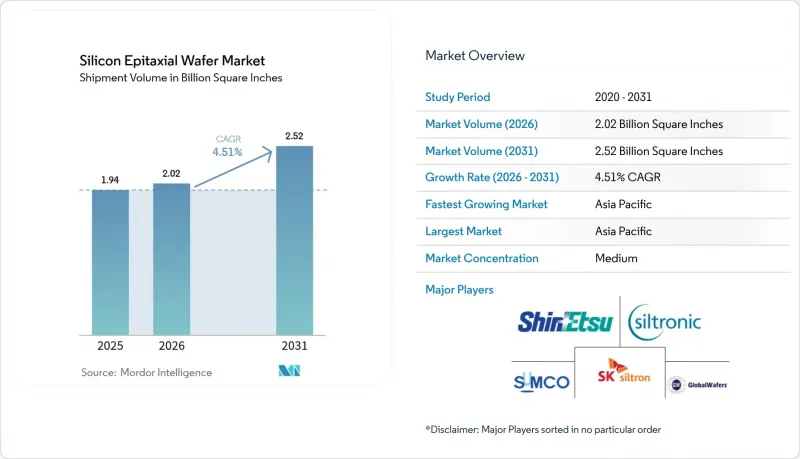
預計矽外延晶片市場將從 2025 年的 193859 億平方英寸和 2026 年的 201827 億平方英寸成長到 2031 年的 251609 億平方英寸,2026 年至 2031 年的複合年成長率為 4.51%。
採用更厚、缺陷更少的300毫米基板底層,以及背面供電技術、汽車電氣化和設備端人工智慧推理日益成長的需求,為生產奠定了堅實的基礎。亞太地區已安裝的反應爐數量、政府補貼和不斷成長的記憶體製造能力,使該地區保持了在生產領域的領先地位;而使用同位素純化Si-28層的量子計算原型,則預示著一個具有重要戰略意義的未來細分市場。擁有八個反應器的300毫米生產線超過1.2億美元的資本投資,加上多晶矽原料價格的波動,迫使小規模的供應商退出市場或進行整合。現有企業正轉向使用可再生能源供電的無塵室和低溫選擇性外延模組,以滿足嚴格的碳足跡審查和低於1.5奈米的光刻套刻精度要求。
全球矽外延晶片市場趨勢及洞察
對300mm邏輯和記憶體產能的需求不斷成長。
晶圓代工廠和半導體製造商承諾在2025年至2026年間投資1,650億美元新建300毫米晶圓廠,其中包括台積電的鳳凰城超級晶圓廠、三星的泰勒晶圓廠和SK海力士的P&T7晶圓廠。到2028年,所有這些晶圓廠每年將需要超過5,000萬平方英吋的外延晶圓,其中每一層2奈米或3奈米邏輯晶圓都需要進行精確調校,以控制閾值電壓的變化。記憶體製造商正在將高頻寬記憶體堆疊技術擴展到12-16層,這需要更薄、經過應力調校的基底晶圓,以防止在穿透矽通孔(TSV)鑽孔過程中發生翹曲。這種邏輯和記憶體一體化的流水線將穩定需求基準,使供應商免受拋光晶圓需求劇烈波動的影響。英特爾和台積電的背面供電(BPD)藍圖將進一步降低300毫米直徑晶圓的公差至±1%。
半導體裝置的小型化推動了對超低缺陷密度外延晶片的需求。
環柵電晶體(GAAA)技術興起於3nm工藝,並在2nm製程階段臻於成熟,其允許的缺陷密度可降低至0.01 cm⁻²以下,相比鰭式場效電晶體(FinFET)增加了10倍。垂直奈米片堆疊結構會放大單一位錯造成的損傷,並使驅動電流降低高達15%。供應商目前正透過將原位氫退火與超高純度前驅體相結合來實現製程節點的轉換,但這會增加資本投入。隨著電源軌和接地軌設計規則的日益嚴格,外延層應力(例如極強紫外線照射)的不利影響也越來越顯著。由於這些經濟差異,高階超低缺陷產品的價格溢價高達30%至50%,同時,長期、更具約束力的合約也應運而生。
擴大對 300 毫米外延反應器和自動化設備的資本投資。
一台300毫米CVD反應器的成本在1200萬美元到1500萬美元之間,而一條新的生產線需要8到12台反應器,外加價值3000兆美元到5000兆美元的自動化設備,因此在潔淨室安裝之前,初始投資約為1.5億美元到1.7億美元。正如Siltronic公司於2025年7月停止生產150毫米設備所顯示的那樣,小規模的製造商正努力分攤這筆費用。從2024年到2025年,利率上升推高了加權平均資本成本(WACC)。這項變化延緩了一些企業的擴張計劃,並使資產負債表上現金充裕的成熟大型企業處於有利地位。
細分市場分析
到2025年,300毫米級晶圓的出貨量將佔總出貨量的68.49%,這反映了其在尖端製程節點中的核心地位,並為外延矽晶圓市場規模樹立了標竿。背面供電技術使晶圓層厚度增加了15-20%,提高了信越化學和SUMCO等公司的反應器運轉率。自2023年以來,SEMI已將平整度和翹曲的公差限制收緊了30%,迫使供應商升級其測量技術和製程控制。同時,老舊晶圓廠的維修浪潮正推動200毫米晶圓的需求持續以4.95%的複合年成長率成長,與先前預測的需求下降趨勢截然相反。 Okmetic斥資4億歐元(約4.52億美元)在Vantaa工廠擴建,計劃於2026年運作,這將使其200毫米晶圓的汽車感測器和混合訊號整合電路產能翻倍。同時,WaferWorks和Episil也在擴大其200毫米晶圓的產能。儘管小於150毫米晶圓的市場規模正在萎縮,但一些小眾光電製造商仍在維持其專業化的生產能力。
200mm市場的成長動能主要由汽車產業推動,功率模組製造商正在改造其生產線,以生產碳化矽(SiC)閘極驅動器和ADAS感測器IC。中國在成熟節點技術方面力求自給自足的努力也進一步促進了200mm晶圓的產量成長。同時,300mm晶圓的投資仍集中在亞太地區,鞏固了該地區在矽外延片市場的主導地位。
《矽外延晶圓市場報告》依晶圓直徑(150毫米及以下,200毫米及以上)、半導體裝置類型(邏輯裝置、記憶體及其他)、終端用戶產業(家用電子電器、汽車、工業及其他)及地區進行細分。市場預測以體積(平方英吋)為單位。
區域分析
亞太地區預計在2025年將佔全球出貨量的80.41%,並預計到2031年將以5.58%的複合年成長率成長。台灣在先進邏輯裝置生產方面處於領先地位,韓國主導著記憶體市場,而中國的自給自足計劃正在增加對成熟製程節點的需求;所有這些因素共同支撐著該地區在矽外延片市場中的佔有率。日本向台積電熊本工廠和Rapidus提供的68億美元援助計畫確保了國內供應的連續性,同時,由於中國出口限制的風險,日本晶圓廠正在增加庫存。位於印度古吉拉突邦的計畫將成為未來發展的立足點,但預計初期晶圓仍需進口。
預計到2025年,北美市佔率將維持在5%左右,但得益於《晶片與科學法案》的津貼。 GlobalWafers位於謝爾曼的工廠(已於2025年5月投產)和英特爾位於俄亥俄州的巨型晶圓廠預計到2028年將合計產生超過1000萬平方英寸的年需求量。歐洲在成本和授權方面落後於北美,但Siltronic位於新加坡的300毫米生產線和GlobalWafers位於義大利諾瓦拉的工廠(已於2025年10月投產,並獲得4億歐元(4.52億美元)的補貼)正在為汽車行業確保供應管道。與中東和非洲一樣,南美洲仍嚴重依賴進口,短期內擴大本地產能的前景有限。
區域集中度的提高引發了人們對亞太地區戰略依賴性增強的擔憂,這可能導致補貼競爭和出口限制。然而,亞太地區在反應器部署方面的經驗、製程技術以及叢集經濟效應,將確保其在未來十年繼續主導外延矽晶片市場。
其他好處:
- Excel格式的市場預測(ME)表
- 3個月的分析師支持
目錄
第1章:引言
- 研究假設和市場定義
- 調查範圍
第2章:調查方法
第3章執行摘要
第4章 市場狀況
- 市場概覽
- 產業價值鏈分析
- 監理情勢
- 宏觀經濟因素的影響
- 技術分析
- 波特五力分析
- 供應商的議價能力
- 買方的議價能力
- 新進入者的威脅
- 替代品的威脅
- 競爭公司之間的競爭
- 市場促進因素
- 半導體裝置的小型化推動了對超低缺陷密度外延晶片的需求。
- 對300mm邏輯和記憶體產能的需求不斷成長。
- 汽車ADAS和電力電子產品的激增對高品質外延層的需求日益成長
- 亞太地區政府對國內300毫米晶圓製造廠的補貼
- 採用背面供電架構正在推動對外延層厚度的需求增加。
- 同位素純化的Si-28外延層中量子計算量子位元的出現。
- 市場限制因素
- 增加對 300 毫米外延反應器和自動化設備的資本投入。
- 矽原料價格波動對晶圓利潤率帶來壓力。
- 由於外延應力不匹配導致的光刻圖案崩壞。
- 對高能耗化學氣相沉積外延製程的碳足跡進行審查
第5章 市場規模與成長預測
- 依晶圓直徑
- 最大可達 150 毫米
- 200 mm
- 300 mm
- 依半導體裝置類型
- 邏輯
- 記憶
- 模擬
- 離散的
- 其他半導體裝置類型(光電子裝置、感測器、微型元件)
- 最終用戶
- 家用電子電器
- 手機和智慧型手機
- 個人電腦和伺服器
- 工業的
- 溝通
- 車
- 其他終端用戶應用程式
- 家用電子電器
- 按地區
- 北美洲
- 美國
- 加拿大
- 墨西哥
- 歐洲
- 德國
- 英國
- 法國
- 其他歐洲國家
- 亞太地區
- 中國
- 日本
- 印度
- 韓國
- 台灣
- 亞太其他地區
- 南美洲
- 中東和非洲
- 北美洲
第6章 競爭情勢
- 市場集中度
- 策略趨勢
- 市佔率分析
- 公司簡介
- Shin-Etsu Handotai Co. Ltd.
- SUMCO Corporation
- GlobalWafers Co. Ltd.
- Siltronic AG
- SK Siltron Co. Ltd.
- Okmetic Oyj
- Wafer Works Corporation
- Poshing Silicon Co. Ltd.
- Simgui Shanghai
- Hebei Semiconductor
- Soitec SA
- Episil Technologies Inc.
- MCL Electronic Materials Ltd.
- Siltronix Silicon Technologies
- Advanced Micro-Fabrication Equipment Inc.
- Ferrotec Holdings Corporation
- Topco Scientific Co. Ltd.
- Nova Electronic Materials LLC
- Shenhe Thermo-Magnetics Electronics Co.
- Addison Engineering Inc.
- Virginia Semiconductor Inc.
第7章 市場機會與未來展望
The epitaxial silicon wafer market size is projected to expand from 1,938.59 million square inches in 2025, 2,018.27 million square inches in 2026, to 2,516.09 million square inches by 2031, registering a 4.51% CAGR over 2026-2031.
Thicker, ultra-low-defect layers for 300 mm substrates, backside-power-delivery adoption, and rising demand from automotive electrification and on-device AI inference together underpin a durable volume floor. Asia-Pacific's installed reactor base, government subsidies, and memory-capability additions keep regional output dominant, while quantum-computing prototypes on isotopically purified Si-28 layers point to a strategically important future niche. Capital expenditure above USD 120 million for an eight-reactor 300 mm line, coupled with volatile polysilicon feedstock pricing, pushes smaller suppliers to exit or consolidate. Incumbents are moving to renewable-powered cleanrooms and lower-temperature selective-epitaxy modules to satisfy carbon-footprint scrutiny and lithography overlay budgets below 1.5 nm.
Global Silicon Epitaxial Wafer Market Trends and Insights
Rising Demand for 300 mm Logic and Memory Capacity Expansions
Foundries and integrated device makers pledged USD 165 billion to new 300 mm fabs during 2025-2026, including TSMC's Phoenix megafab, Samsung's Taylor facility, and SK Hynix's P&T7 plant. Together, these sites will require more than 50 million square inches of epitaxial wafers annually by 2028, and each 2 nm or 3 nm logic wafer needs a rigorously tuned layer to control threshold-voltage spread. Memory producers are stretching high-bandwidth-memory stacks to 12-16 layers, demanding thinner base wafers with engineered stress to avoid warpage in through-silicon-via drilling. The combined logic-memory pipeline stabilizes baseline demand and shields suppliers from the polished-wafer boom-bust pattern. Intel and TSMC's backside-power-delivery roadmaps further compress tolerance to +-1% across a 300 mm-diameter.
Semiconductor Device Scaling Driving Demand for Ultra-Low-Defect Density Epi Wafers
Gate-all-around transistors debuting at 3 nm and maturing at 2 nm cut the allowable defect density to below 0.01 cm-2, a tenfold tightening compared to fin-FETs. Vertical nanosheet stacks amplify the damage caused by single dislocations, reducing drive current by up to 15%. Suppliers now pair in-situ hydrogen anneals with ultra-high-purity precursors, raising capital intensity but enabling node transitions. Reducing design rules for power and ground rails magnifies the penalty for epi-induced stress during extreme-ultraviolet exposure. The economic split pushes premium ultra-low-defect products to command 30-50% price premiums as stickier, longer contracts emerge.
Escalating Capex for 300 mm Epitaxy Reactors and Automation
A single 300 mm CVD reactor costs USD 12-15 million, and a greenfield line requires 8-12 reactors, plus USD 30-50 million in automation, bringing upfront investment to roughly USD 150-170 million before cleanroom fit-out. Smaller producers struggle to amortize that load, as Siltronic's July 2025 exit from 150 mm production showed. In 2024-2025, rising interest rates led to an increase in the weighted-average cost of capital. This shift resulted in delays for certain expansions and favored established players who could leverage their balance-sheet cash.
Other drivers and restraints analyzed in the detailed report include:
- Surge in Automotive ADAS and Power Electronics Requiring High-Quality Epi Layers
- Government Subsidies for Domestic 300 mm Wafer Fabs in Asia-Pacific
- Volatile Silicon Feedstock Prices Compressing Wafer Margins
For complete list of drivers and restraints, kindly check the Table Of Contents.
Segment Analysis
The 300 mm class delivered 68.49% of shipments in 2025, reflecting its centrality to leading-edge nodes and setting the baseline for the epitaxial silicon wafer market size. Backside power delivery lifts layer thickness by 15-20%, driving higher reactor utilization at Shin-Etsu and SUMCO. SEMI tightened flatness and bow limits by 30% since 2023, compelling suppliers to upgrade metrology and process control. Conversely, a retrofit wave in older fabs keeps 200 mm demand expanding at a 4.95% CAGR, defying earlier forecasts of terminal decline. Okmetic's EUR 400 million (USD 452 million) Vantaa expansion, operational in 2026, doubled 200 mm capacity to serve automotive sensors and mixed-signal ICs, while Wafer Works and Episil also grew 200 mm output. The 150 mm and smaller pool is shrinking, yet niche optoelectronics players retain specialized capacity.
200 mm momentum is heavily automotive-driven, as power-module makers retrofit lines for silicon-carbide gate drivers and ADAS sensor ICs. China's push for self-sufficiency in mature-node technology further elevates 200 mm volumes. Meanwhile, 300 mm investments stay concentrated in Asia-Pacific, cementing the region's dominance in the epitaxial silicon wafer market.
The Silicon Epitaxial Wafer Market Report is Segmented by Wafer Diameter (Up To 150 Mm, 200 Mm, and More), Semiconductor Device Type (Logic, Memory, and More), End-User Industry (Consumer Electronics, Automotive, Industrial, and More), and Geography. The Market Forecasts are Provided in Terms of Volume (Square Inches).
Geography Analysis
Asia-Pacific commanded 80.41% of 2025 volume and is projected to expand at a 5.58% CAGR through 2031. Taiwan leads advanced-logic output, South Korea dominates memory, and China's self-reliance plan increases mature-node pulls, together underpinning the region's share of the epitaxial silicon wafer market size. Japan's USD 6.8 billion incentive package for TSMC Kumamoto and Rapidus ensures local supply continuity, while China's export-control risks spur stockpiling by domestic fabs. India's Gujarat project adds a future foothold, though initial wafers will be imported.
North America held a mid-single-digit slice in 2025 but benefits from the CHIPS and Science Act grants. GlobalWafers' Sherman plant, opened in May 2025, and Intel's Ohio megafab will together demand more than 10 million square inches a year by 2028. Europe lags on cost and permitting, yet Siltronic's Singapore 300 mm line and GlobalWafers' Novara, Italy site, opened in October 2025 with EUR 400 million (USD 452 million) in subsidies, secure automotive-focused supply routes. South America, along with the Middle East and Africa, remains import-dependent, with limited near-term prospects for indigenous capacity.
Regional concentration raises strategic-dependency alarms in the United States and Europe, prompting subsidy races and export controls. Still, Asia-Pacific's reactor installed base, process know-how, and cluster economics make its dominance in the epitaxial silicon wafer market difficult to dislodge before the next decade.
- Shin-Etsu Handotai Co. Ltd.
- SUMCO Corporation
- GlobalWafers Co. Ltd.
- Siltronic AG
- SK Siltron Co. Ltd.
- Okmetic Oyj
- Wafer Works Corporation
- Poshing Silicon Co. Ltd.
- Simgui Shanghai
- Hebei Semiconductor
- Soitec S.A.
- Episil Technologies Inc.
- MCL Electronic Materials Ltd.
- Siltronix Silicon Technologies
- Advanced Micro-Fabrication Equipment Inc.
- Ferrotec Holdings Corporation
- Topco Scientific Co. Ltd.
- Nova Electronic Materials LLC
- Shenhe Thermo-Magnetics Electronics Co.
- Addison Engineering Inc.
- Virginia Semiconductor Inc.
Additional Benefits:
- The market estimate (ME) sheet in Excel format
- 3 months of analyst support
TABLE OF CONTENTS
1 INTRODUCTION
- 1.1 Study Assumptions and Market Definition
- 1.2 Scope of the Study
2 RESEARCH METHODOLOGY
3 EXECUTIVE SUMMARY
4 MARKET LANDSCAPE
- 4.1 Market Overview
- 4.2 Industry Value-Chain Analysis
- 4.3 Regulatory Landscape
- 4.4 Impact of Macroeconomic Factors
- 4.5 Technology Analysis
- 4.6 Porter's Five Forces Analysis
- 4.6.1 Bargaining Power of Suppliers
- 4.6.2 Bargaining Power of Buyers
- 4.6.3 Threat of New Entrants
- 4.6.4 Threat of Substitutes
- 4.6.5 Intensity of Competitive Rivalry
- 4.7 Market Drivers
- 4.7.1 Semiconductor Device Scaling Driving Demand for Ultra-Low Defect Density Epi Wafers
- 4.7.2 Rising Demand for 300 mm Logic and Memory Capacity Expansions
- 4.7.3 Surge in Automotive ADAS and Power Electronics Requiring High-Quality Epi Layers
- 4.7.4 Government Subsidies for Domestic 300 mm Wafer Fabs in Asia-Pacific
- 4.7.5 Adoption of Backside-Power-Delivery Architectures Boosting Epi Thickness Needs
- 4.7.6 Emergence of Quantum-Computing Qubits on Isotopically Purified Si-28 Epi Layers
- 4.8 Market Restraints
- 4.8.1 Escalating Capex for 300 mm Epitaxy Reactors and Automation
- 4.8.2 Volatile Silicon Feedstock Prices Compressing Wafer Margins
- 4.8.3 Lithography-Induced Pattern Collapse from Epi Stress Mismatches
- 4.8.4 Carbon-Footprint Scrutiny of Energy-Intensive CVD Epitaxy Processes
5 MARKET SIZE AND GROWTH FORECASTS (VOLUME)
- 5.1 By Wafer Diameter
- 5.1.1 Up to 150 mm
- 5.1.2 200 mm
- 5.1.3 300 mm
- 5.2 By Semiconductor Device Type
- 5.2.1 Logic
- 5.2.2 Memory
- 5.2.3 Analog
- 5.2.4 Discrete
- 5.2.5 Other Semiconductor Device Types (Optoelectronics, Sensors, Micro)
- 5.3 By End-user
- 5.3.1 Consumer Electronics
- 5.3.1.1 Mobile and Smartphones
- 5.3.1.2 PCs and Servers
- 5.3.2 Industrial
- 5.3.3 Telecommunications
- 5.3.4 Automotive
- 5.3.5 Other End-user Applications
- 5.3.1 Consumer Electronics
- 5.4 By Geography
- 5.4.1 North America
- 5.4.1.1 United States
- 5.4.1.2 Canada
- 5.4.1.3 Mexico
- 5.4.2 Europe
- 5.4.2.1 Germany
- 5.4.2.2 United Kingdom
- 5.4.2.3 France
- 5.4.2.4 Rest of Europe
- 5.4.3 Asia-Pacific
- 5.4.3.1 China
- 5.4.3.2 Japan
- 5.4.3.3 India
- 5.4.3.4 South Korea
- 5.4.3.5 Taiwan
- 5.4.3.6 Rest of Asia-Pacific
- 5.4.4 South America
- 5.4.5 Middle East and Africa
- 5.4.1 North America
6 COMPETITIVE LANDSCAPE
- 6.1 Market Concentration
- 6.2 Strategic Moves
- 6.3 Market Share Analysis
- 6.4 Company Profiles (includes Global Level Overview, Market Level Overview, Core Segments, Financials as available, Strategic Information, Market Rank/Share, Products and Services, Recent Developments)
- 6.4.1 Shin-Etsu Handotai Co. Ltd.
- 6.4.2 SUMCO Corporation
- 6.4.3 GlobalWafers Co. Ltd.
- 6.4.4 Siltronic AG
- 6.4.5 SK Siltron Co. Ltd.
- 6.4.6 Okmetic Oyj
- 6.4.7 Wafer Works Corporation
- 6.4.8 Poshing Silicon Co. Ltd.
- 6.4.9 Simgui Shanghai
- 6.4.10 Hebei Semiconductor
- 6.4.11 Soitec S.A.
- 6.4.12 Episil Technologies Inc.
- 6.4.13 MCL Electronic Materials Ltd.
- 6.4.14 Siltronix Silicon Technologies
- 6.4.15 Advanced Micro-Fabrication Equipment Inc.
- 6.4.16 Ferrotec Holdings Corporation
- 6.4.17 Topco Scientific Co. Ltd.
- 6.4.18 Nova Electronic Materials LLC
- 6.4.19 Shenhe Thermo-Magnetics Electronics Co.
- 6.4.20 Addison Engineering Inc.
- 6.4.21 Virginia Semiconductor Inc.
7 MARKET OPPORTUNITIES AND FUTURE OUTLOOK
- 7.1 White-Space and Unmet-Need Assessment
 碳化矽基板和外延晶片的專利趨勢調查
 日本LED外延片:市佔率分析、產業趨勢與統計及成長預測(2026-2031年)AlGaN深紫外LED外延片:市佔率分析、產業趨勢與統計及成長預測(2026-2031年)藍寶石基板氮化鎵LED外延片:市佔率分析、產業趨勢與統計、成長預測(2026-2031年)
 外延晶片市場:按材料、晶片尺寸、應用和產業分類-2026-2032年全球市場預測
 矽外延晶片市場分析及預測(至2035年):依類型、產品、技術、應用、材料類型、裝置、製程、最終用戶及功能分類
 外延晶片市場規模、佔有率、趨勢及預測(按類型、晶片尺寸、應用、產業及地區分類),2026-2034年
 2026年全球矽外延晶片市場報告外延晶片市場-2026-2031年預測
 外延晶片市場:按類型、應用、終端用戶產業、國家及地區分類 - 全球產業分析、市場規模、市場佔有率及2025-2032年預測