


 |
市場調查報告書
商品編碼
2063438
藍寶石基板氮化鎵LED外延片:市佔率分析、產業趨勢與統計、成長預測(2026-2031年)GaN-on-Sapphire LED Epitaxial Wafer - Market Share Analysis, Industry Trends & Statistics, Growth Forecasts (2026 - 2031) |
||||||
※ 本網頁內容可能與最新版本有所差異。詳細情況請與我們聯繫。
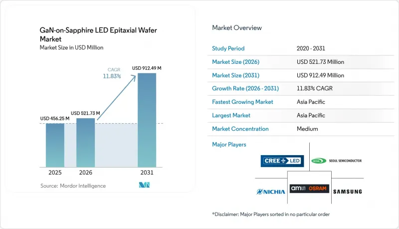
據 Mordor Intelligence 稱,藍寶石上氮化鎵 LED 外延晶片市場預計將從 2025 年的 4.5625 億美元成長到 2026 年的 5.2173 億美元,到 2031 年達到 9.1249 億美元,2026 年成長率為 2031 年的複合年成長率為 1.83%。
本報告按晶圓直徑(小於100毫米、150毫米、大於200毫米)、應用領域(通用照明、汽車照明、顯示和背光、特殊和工業照明)以及地區進行細分。市場預測以美元(USD)為單位。
全球藍寶石基板氮化鎵LED外延晶圓市場趨勢及洞察
迷你LED和微型LED顯示器的廣泛應用
目前,高階電視品牌每塊面板整合了10,000到25,000顆mini-LED晶片,實現了超過2,000個局部調光區域,這是側入式背光無法實現的。 Ennostar計畫於2025年完成合併,屆時將把400多個金屬有機化學氣相沉積(MOCVD)反應器整合到單一供應鏈中,確保向蘋果和三星供應晶圓,同時加強對外延製程的控制。 PlayNitride和Plessey正在藍寶石基板上採用單片micro-LED陣列,以避免混合矽背板系統因質傳而導致的良率下降,使這項技術有望應用於擴增實境(AR)頭顯。汽車駕駛座也朝著亮度超過每平方公尺10,000坎德拉的micro-LED叢集發展,即使在陽光下也清晰可見。由於散熱限制,傳統的磷光體轉換白光LED難以達到此規格。這些進步結合起來,正在創造對均勻的藍寶石上氮化鎵外延晶片的持續需求,這種晶片能夠支援精確的波長分檔和低正向電壓變化。
無需使用磷光體即可快速過渡到超高亮度照明
建築和園藝照明燈具正轉向直接髮射紅、綠、藍光的叢集,這種陣列消除了使用黃色磷光體進行降壓轉換器時造成的15-25%的能量損失。一項發表於2024年的研究表明,藍寶石基板上量子阱的外部量子效率,藍色光可達52.4%,綠色光可達25.2%,幾乎是2010年性能基準的兩倍。將於2025年1月生效的歐盟生態設計指令要求在2027年將最低光通量效率提高到每瓦210流明,這加速了人們對無需複雜溫度控管即可實現這一目標的無磷光體陣列的興趣。三安光電已將其在湖北省116億元人民幣擴張計畫中的40%用於開發針對園藝應用最佳化的窄頻紅綠晶片,凸顯了商業性對這些高亮度元件的巨大需求。監管壓力、量子阱效率的提高以及產能的擴大,共同促成了無磷光體照明成為藍寶石基板上氮化鎵晶片的永續成長引擎。
由於尺寸超過 200mm 時熱膨脹係數不匹配,導致產量降低。
藍寶石(7.5 × 10⁻⁶ K⁻¹)和氮化鎵(5.6 × 10⁻⁶ K⁻¹)的熱膨脹係數差異會導致厚度超過 5 µm 的外延層中產生 -1.0 至 -1.5 GPa 的殘餘應力發生率,從而增加 200 mm 微翹曲和開晶的殘餘應力發生率。 2024 年 12 月的一項奈米材料研究表明,當 200 mm 藍寶石晶圓上的 GaN 厚度超過 20 µm 時,觀察到宏觀裂紋密度超過 0.3 cm⁻²,使得此類晶圓不適用於高功率LED。圖案化基板和軟性 AlN 緩衝層可以將翹曲減小到 50 µm 以下,但這會使週期時間增加 15-20%,並且還會增加耗材成本。因此,儘管200毫米晶圓在面積優勢高達78%,顯示器製造商仍堅持為mini-LED背光燈指定150毫米晶圓。在應力管理技術成熟之前,小直徑晶圓在晶圓層面上更具經濟優勢,因此短期過渡計畫受到限制。
細分市場分析
2025年,150mm規格的晶圓將佔藍寶石基氮化鎵LED外延晶圓市場48.78%的佔有率。這反映了面積產能與位錯密度(3 × 10⁸ 至 5 × 10⁸ cm⁻²)之間的平衡。這種均勻性對於汽車自我調整光束模組至關重要,因為它可以將正向電壓波動控制在±50 mV以內,即使在千赫茲級驅動頻率下也能保持熱預算可控。 Ennostar公司400多台MOCVD系統仍維持150mm規格。這是因為將單一反應器升級到200mm規格需要花費200萬至300萬美元,並且會擾亂已認證的製程。 Veeco公司的Propel300平台採用8x150mm配置,產能提升20%,在維持大直徑晶圓成本優勢的同時,降低了每片晶圓的折舊免稅額成本。因此,儘管 150 毫米晶圓的 GaN-on-sapphire LED 外延晶圓市場佔有率將會下降,但預計該市場仍將是預測期中期之前的收入支柱。
為了將單片晶圓面積提高 78%,預計到 2031 年,尺寸大於 200 mm 的晶圓採用率將以 12.84% 的複合年成長率成長。然而,當 GaN 厚度超過 20 µm 時,殘餘壓應力通常會超過 -1.2 GPa,宏觀裂紋密度也會增加到 0.3 cm⁻² 以上。圖案化藍寶石基板和軟性 AlN 緩衝層可以將翹曲度降低到 50 µm 以下,但這會使製程時間增加 15%–20%,抵消了每個晶片的成本節省。 UVC(紫外線 C)LED 的尺寸可達 100 mm,透過嚴格控制鋁成分,攜帶式消毒器在 265 nm 波長的電光轉換效率可超過 5%。設備供應商支援5片200毫米晶圓的批量處理,但早期用戶反映,缺陷造成的廢品,尤其是在高功率晶片中,很大程度上抵消了理論上的成本優勢。在良率工程方面取得突破性進展之前,買家仍將繼續把訂單拆分,成熟產品使用150毫米晶圓,而尖端顯示器則使用200毫米晶圓,因此藍寶石基氮化鎵LED外延晶圓市場的佔有率波動可能有限。
區域分析
到2025年,亞太地區將佔全球銷售額的66.85%,該地區的藍寶石基板氮化鎵LED外延晶圓市場預計到2031年將以12.75%的複合年成長率成長。台灣是出口中心,恩諾斯達(Ennostar)在2025年合併後,將在多個地點運作超過400套金屬有機化學氣相沉積(MOCVD)系統。中國也緊跟其後,三安光電預計到2025年將處理約2,400萬片晶圓,並投資116億元擴建其位於湖北省的mini-LED園區。在日本,一項津貼計畫涵蓋化合物半導體晶圓廠高達50%的成本,正在推動日亞化學工業株式會社(Nichia Corporation)向藍寶石基板垂直整合,從而保護該地區免受原料價格飆升的影響。這些努力加在一起,有望在整個預測期內保持亞太地區在藍寶石上氮化鎵LED外延晶片市場的主導地位。
在北美,《晶片與科學法案》正為國內晶圓廠帶來520億美元的資金,再次鞏固其市場地位。 Veeco Instruments宣布將於2024年推出新的外延生產,並向一家美國電力電子客戶交付了首套Propel300 GaN系統。三安電子計畫以2.39億美元收購Lumileds,這將把北美汽車照明合約整合到中國的供應鏈中,進一步深化該地區的一體化。這些發展預計在2020年代末期提升北美地區在藍寶石基板氮化鎵LED外延晶圓市場的佔有率,但在可預見的未來,對亞洲基板進口的依賴仍將是一個阻礙因素。
儘管歐洲在2025年的銷售額中所佔佔有率較小,但它正受益於430億歐元的“晶片法案”,該法案為氮化鎵和碳化矽生產線撥款。歐司朗的EVIYOS自適應光束平台象徵著該地區對高價值汽車晶片的重視,這些晶片足以支撐其較高的晶圓價格。德國、荷蘭和法國的垂直農業計畫正在採用園藝用微型LED陣列,推動了對特殊應用的需求。世界其他地區,特別是拉丁美洲和中東及非洲,仍在發展中,但紫外線C(UVC)水處理試點計畫正在取得進展,藍寶石相對於矽的熱優勢在該領域至關重要。雖然這些地區對整體銷售量的成長做出了貢獻,但它們不太可能撼動亞太地區在藍寶石基氮化鎵LED外延晶圓市場的主導地位。
其他好處:
- Excel格式的市場預測(ME)表
- 3個月的分析師支持
目錄
第1章:引言
- 研究假設和市場定義
- 調查範圍
第2章:調查方法
第3章執行摘要
第4章 市場狀況
- 市場促進因素
- Mini-LED 和 Micro-LED 顯示器的廣泛應用
- 無需使用磷光體即可快速過渡到超高亮度照明
- 150毫米藍寶石上氮化鎵晶圓的成本下降趨勢
- 政府對化合物半導體製造的激勵措施
- 在UV-C殺菌LED中採用GaN外延層
- 將GaN LED整合到Li-Fi光纖通訊中
- 市場限制因素
- 由於熱失配超過 200 毫米,導致產量下降。
- 高純度藍寶石基板的供應限制
- 用於形成均勻厚度GaN層的資本密集型MOCVD設備
- 在電視背光市場,面臨來自新興的GaN-on-Si平台的競爭。
- 產業分析
- 宏觀經濟因素對市場的影響
- 技術分析
- 波特五力分析
第5章 市場規模與成長預測
- 依晶圓直徑
- 100毫米或更小
- 150 mm
- 200毫米或以上
- 透過使用
- 一般照明
- 汽車照明
- 顯示器和背光
- 特殊和工業照明
- 按地區
- 北美洲
- 歐洲
- 亞太地區
- 世界其他地區
第6章 競爭情勢
- 市場集中度
- 策略趨勢
- 市佔率分析
- 公司簡介
- Nichia Corporation
- Osram Opto Semiconductors GmbH
- Cree LED, Inc.
- Samsung LED Co., Ltd.
- Seoul Semiconductor Co., Ltd.
- Epistar Corporation
- San'an Optoelectronics Co., Ltd.
- HC SemiTek Corporation
- Plessey Semiconductors Ltd.
- LG Innotek Co., Ltd.
- Lumileds Holding BV
- Bridgelux, Inc.
- Lextar Electronics Corp.
- Silanna Semiconductor Pty Ltd.
- Aledia SA
- Opto Tech Corporation
- PlayNitride Inc.
- Tianma Microelectronics Co., Ltd.
- Innolux Corporation
- Veeco Instruments Inc.
第7章 市場機會與未來展望
According to Mordor Intelligence, the gaN-on-Sapphire lED epitaxial wafer market size is expected to increase from USD 456.25 million in 2025 to USD 521.73 million in 2026 and reach USD 912.49 million by 2031, growing at a CAGR of 11.83% over 2026-2031.
This report is Segmented by Wafer Diameter (Up To 100 Mm, 150 Mm, 200 Mm and Above), Application (General Lighting, Automotive Lighting, Display and Backlighting, Specialty and Industrial Lighting), and Geography. The Market Forecasts are Provided in Terms of Value (USD).
Global GaN-on-Sapphire LED Epitaxial Wafer Market Trends and Insights
Increasing Penetration of Mini and Micro-LED Displays
Premium television brands now mount between 10,000 and 25,000 mini-LED dies per panel, unlocking more than 2,000 local-dimming zones that edge-lit backlights cannot match. Ennostar's 2025 merger integrated over 400 metal-organic chemical-vapor-deposition (MOCVD) reactors into a single supply chain, ensuring wafer availability for Apple and Samsung and tightening epitaxial process control. PlayNitride and Plessey use monolithic micro-LED arrays on sapphire to bypass the mass-transfer yield losses that plague hybrid silicon-backplane approaches, positioning their technology for augmented-reality headsets. Automotive cockpits are also shifting to micro-LED clusters that achieve daylight-readable luminance above 10,000 candelas per square meter, a specification conventional phosphor-converted white LEDs struggle to meet within thermal limits. Together, these deployments create sustained demand for uniform GaN-on-sapphire epitaxial wafers that support tight wavelength binning and low forward-voltage spread.
Rapid Shift Toward Phosphor-Free Ultra-High-Brightness Lighting
Architectural and horticultural fixtures are migrating to direct-emission red-green-blue clusters that eliminate the 15-25% energy loss from yellow-phosphor down-conversion. Research published in 2024 showed external quantum efficiencies reaching 52.4% for blue and 25.2% for green quantum wells on sapphire, roughly doubling 2010 performance benchmarks. Europe's Ecodesign Directive, active since January 2025, raises minimum efficacy to 210 lumens per watt by 2027, accelerating interest in phosphor-free arrays that meet the target without complex thermal management. San'an Optoelectronics earmarked 40% of its CNY 11.6 billion Hubei expansion for narrow-band red and green dies optimized for horticulture, underlining the commercial pull of these higher-brightness devices. The convergence of regulatory pressure, quantum-well efficiency gains, and capacity expansions positions phosphor-free lighting as a durable growth engine for GaN-on-sapphire wafers.
Thermal Mismatch-Driven Yield Losses Above 200 mm
Sapphire's thermal-expansion coefficient of 7.5 X 10⁻⁶ K-1 versus gallium-nitride's 5.6 X 10⁻⁶ K-1 induces residual compressive stress between -1.0 and -1.5 GPa in epilayers thicker than 5 µm, increasing bow and crack rates on 200 mm wafers. December 2024 Nanomaterials research documented macro-crack densities above 0.3 cm-2 when the GaN thickness exceeded 20 µm on 200 mm sapphire wafers, rendering such wafers unsuitable for high-power LEDs. Patterned substrates and compliant AlN buffers mitigate bow below 50 µm but add 15-20% cycle time and raise consumable costs. Display manufacturers, therefore, continue to specify 150 mm wafers for mini-LED backlights despite the 78% area advantage of 200 mm formats. Until stress-management techniques mature, wafer-level economics favor smaller diameters, tempering near-term transition plans.
Other drivers and restraints analyzed in the detailed report include:
- Cost Downward Trend in 150 mm GaN-on-Sapphire Wafers
- Government Incentives for Compound-Semiconductor Fabs
- Supply Constraints of High-Purity Sapphire Substrates
For complete list of drivers and restraints, kindly check the Table Of Contents.
Segment Analysis
The 150 mm format captured 48.78% of GaN-on-Sapphire LED Epitaxial Wafer market share in 2025, reflecting its balance between area throughput and threading-dislocation densities that stay within the 3 X 10⁸-5 X 108 cm-2 range. Automotive adaptive-beam modules value this uniformity because forward-voltage spread remains under +-50 mV, keeping thermal budgets manageable at kilohertz drive frequencies. Ennostar's fleet of more than 400 MOCVD chambers is still tooled for 150 mm, as retrofitting a single reactor to 200 mm costs USD 2-3 million and disrupts qualified process flows. Veeco's Propel300 platform delivers 20% throughput in its 8X150 mm configuration, reducing depreciation per wafer and locking in the cost advantage of the larger diameter. As a result, the GaN-on-Sapphire LED Epitaxial Wafer market size for 150 mm wafers is expected to remain the revenue anchor through the middle of the forecast window, even though its proportional share declines.
Adoption of 200 mm and larger wafers is projected to rise at a 12.84% CAGR to 2031 as display makers seek the 78% area gain per slice, yet residual compressive stress often exceeds -1.2 GPa and elevates macro-crack density beyond 0.3 cm-2 when GaN exceeds 20 µm. Patterned-sapphire substrates and compliant AlN buffers reduce bow below 50 µm but add 15-20% process time, muting the per-die savings. Up to 100 mm formats are available for ultraviolet-C LEDs, with tight control of aluminum composition enabling≥5% wall-plug efficiency at 265 nm for portable sterilizers. Equipment vendors support 5X200 mm batch loads, yet early adopters report that defect-attributed scrap negates much of the theoretical cost benefit, especially for high-power dies. Until yield-engineering breakthroughs emerge, buyers will continue to split orders between 150 mm for mature products and 200 mm for bleeding-edge displays, limiting abrupt share shifts within the GaN-on-Sapphire LED Epitaxial Wafer market.
Geography Analysis
Asia-Pacific accounted for 66.85% of global revenue in 2025, and the regional GaN-on-Sapphire LED Epitaxial Wafer market is projected to grow at a 12.75% CAGR through 2031. Taiwan anchors exports, with Ennostar operating more than 400 metal-organic chemical-vapor-deposition reactors across multiple sites after its 2025 merger. China complements this scale; San'an Optoelectronics processed about 24 million wafers in 2025 and is investing CNY 11.6 billion to ramp a Hubei mini-LED campus. Japan's subsidy program covering up to 50% of compound-semiconductor fab costs underpins Nichia's vertical move into sapphire substrates, helping shield the region from raw-material shocks. Together, these initiatives preserve Asia-Pacific's lead in the GaN-on-Sapphire LED Epitaxial Wafer market size over the forecast horizon.
North America is regaining footing as the CHIPS and Science Act channels USD 52 billion into domestic fabs. Veeco Instruments shipped its first Propel300 GaN system to a U.S. power-electronics customer in 2024, signaling the launch of fresh epitaxial capacity. San'an's planned USD 239 million acquisition of Lumileds folds North American automotive-lighting contracts into a Chinese supply chain, boosting the region's integration depth. These moves could lift the continent's GaN-on-Sapphire LED Epitaxial Wafer market share by the late 2020s, although reliance on Asian substrate imports remains a near-term constraint.
Europe captured a modest slice of 2025 revenue but benefits from the EUR 43 billion Chips Act, which allocates funds for gallium nitride and silicon carbide lines. Osram's EVIYOS adaptive-beam platform exemplifies the region's focus on high-value automotive dies that justify premium wafer pricing. Vertical-farming projects across Germany, the Netherlands, and France are adopting horticultural mini-LED arrays, driving specialty demand. The rest of the World, Latin America, the Middle East, and Africa remain nascent, yet pilot ultraviolet-C water-treatment schemes are creating beachheads where sapphire's thermal advantage over silicon is critical. Collectively, these pockets contribute incremental volume but are unlikely to displace Asia-Pacific's dominance in the GaN-on-Sapphire LED Epitaxial Wafer market.
- Nichia Corporation
- Osram Opto Semiconductors GmbH
- Cree LED, Inc.
- Samsung LED Co., Ltd.
- Seoul Semiconductor Co., Ltd.
- Epistar Corporation
- San'an Optoelectronics Co., Ltd.
- HC SemiTek Corporation
- Plessey Semiconductors Ltd.
- LG Innotek Co., Ltd.
- Lumileds Holding B.V.
- Bridgelux, Inc.
- Lextar Electronics Corp.
- Silanna Semiconductor Pty Ltd.
- Aledia SA
- Opto Tech Corporation
- PlayNitride Inc.
- Tianma Microelectronics Co., Ltd.
- Innolux Corporation
- Veeco Instruments Inc.
Additional Benefits:
- The market estimate (ME) sheet in Excel format
- 3 months of analyst support
TABLE OF CONTENTS
1 INTRODUCTION
- 1.1 Study Assumptions and Market Definition
- 1.2 Scope of the Study
2 RESEARCH METHODOLOGY
3 EXECUTIVE SUMMARY
4 MARKET LANDSCAPE
- 4.1 Market Drivers
- 4.1.1 Increasing Penetration of Mini and Micro-LED Displays
- 4.1.2 Rapid Shift Toward Phosphor-Free Ultra-High-Brightness Lighting
- 4.1.3 Cost Downward Trend in 150 mm GaN-on-Sapphire Wafers
- 4.1.4 Government Incentives for Compound-Semiconductor Fabs
- 4.1.5 Adoption of GaN Epilayers for UV-C Sterilization LEDs
- 4.1.6 Integration of GaN LEDs in Li-Fi Optical Communications
- 4.2 Market Restraints
- 4.2.1 Thermal Mismatch-Driven Yield Losses Above 200 mm
- 4.2.2 Supply Constraints of High-Purity Sapphire Substrates
- 4.2.3 Capital-Intensive MOCVD Tooling for Uniform Thick GaN Layers
- 4.2.4 Competition from Emerging GaN-on-Si Platforms in TV Backlighting
- 4.3 Industrial Analysis
- 4.4 Impact of Macroeconomic Factors on the Market
- 4.5 Technology Analysis
- 4.6 Porter's Five Forces Analysis
- 4.6.1 Bargaining Power of Suppliers
- 4.6.2 Bargaining Power of Buyers
- 4.6.3 Threat of New Entrants
- 4.6.4 Threat of Substitutes
- 4.6.5 Intensity of Competitive Rivalry
5 MARKET SIZE AND GROWTH FORECASTS (VALUE)
- 5.1 By Wafer Diameter
- 5.1.1 Upto 100 mm
- 5.1.2 150 mm
- 5.1.3 200 mm and Above
- 5.2 By Application
- 5.2.1 General Lighting
- 5.2.2 Automotive Lighting
- 5.2.3 Display and Backlighting
- 5.2.4 Specialty and Industrial Lighting
- 5.3 By Geography
- 5.3.1 North America
- 5.3.2 Europe
- 5.3.3 Asia-Pacific
- 5.3.4 Rest of the World
6 COMPETITIVE LANDSCAPE
- 6.1 Market Concentration
- 6.2 Strategic Moves
- 6.3 Market Share Analysis
- 6.4 Company Profiles (includes Global Level Overview, Market Level Overview, Core Segments, Financials as available, Strategic Information, Market Rank/Share, Products and Services, Recent Developments)
- 6.4.1 Nichia Corporation
- 6.4.2 Osram Opto Semiconductors GmbH
- 6.4.3 Cree LED, Inc.
- 6.4.4 Samsung LED Co., Ltd.
- 6.4.5 Seoul Semiconductor Co., Ltd.
- 6.4.6 Epistar Corporation
- 6.4.7 San'an Optoelectronics Co., Ltd.
- 6.4.8 HC SemiTek Corporation
- 6.4.9 Plessey Semiconductors Ltd.
- 6.4.10 LG Innotek Co., Ltd.
- 6.4.11 Lumileds Holding B.V.
- 6.4.12 Bridgelux, Inc.
- 6.4.13 Lextar Electronics Corp.
- 6.4.14 Silanna Semiconductor Pty Ltd.
- 6.4.15 Aledia SA
- 6.4.16 Opto Tech Corporation
- 6.4.17 PlayNitride Inc.
- 6.4.18 Tianma Microelectronics Co., Ltd.
- 6.4.19 Innolux Corporation
- 6.4.20 Veeco Instruments Inc.
7 MARKET OPPORTUNITIES AND FUTURE OUTLOOK
- 7.1 White-Space and Unmet-Need Assessment
 碳化矽基板和外延晶片的專利趨勢調查
 日本LED外延片:市佔率分析、產業趨勢與統計及成長預測(2026-2031年)AlGaN深紫外LED外延片:市佔率分析、產業趨勢與統計及成長預測(2026-2031年)
 外延晶片市場:按材料、晶片尺寸、應用和產業分類-2026-2032年全球市場預測矽外延片:市佔率分析、產業趨勢與統計、成長預測(2026-2031)
 矽外延晶片市場分析及預測(至2035年):依類型、產品、技術、應用、材料類型、裝置、製程、最終用戶及功能分類
 外延晶片市場規模、佔有率、趨勢及預測(按類型、晶片尺寸、應用、產業及地區分類),2026-2034年
 2026年全球矽外延晶片市場報告外延晶片市場-2026-2031年預測
 外延晶片市場:按類型、應用、終端用戶產業、國家及地區分類 - 全球產業分析、市場規模、市場佔有率及2025-2032年預測