

 |
市場調查報告書
商品編碼
2063399
邏輯裝置用矽晶圓:市場佔有率分析、產業趨勢與統計資料以及成長預測(2026-2031 年)Silicon Wafer For Logic Devices - Market Share Analysis, Industry Trends & Statistics, Growth Forecasts (2026 - 2031) |
||||||
※ 本網頁內容可能與最新版本有所差異。詳細情況請與我們聯繫。
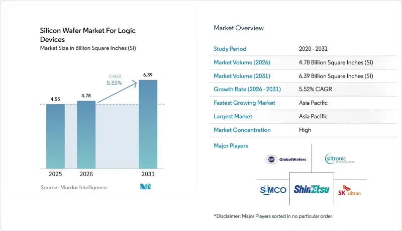
根據 Mordor Intelligence 預測,邏輯裝置用矽晶圓市場規模預計在 2025 年達到 45.3 億平方英寸,在 2026 年達到 47.8 億平方英寸,在 2031 年達到 63.9 億平方英寸。
預計從 2026 年到 2031 年,其複合年成長率將達到 5.52%。
本報告按晶圓直徑(150毫米及以下、200毫米、300毫米)、晶圓類型(拋光晶圓、外延晶圓、絕緣體上矽(SOI)晶圓、特種矽晶圓(高阻矽、功率矽等))、終端用戶應用(消費性電子、工業、電信、汽車等)細分。市場預測以出貨面積(十億平方英吋)為單位。
邏輯裝置矽晶圓市場的趨勢與發展
對人工智慧和高效能運算晶片的需求不斷成長
超大規模資料中心業者正在為規模日益龐大的訓練叢集交付客製化加速器。由於GPU、網路和晶片基片均源自300mm矽晶圓,每個叢集每季可能消耗超過10,000片基板。晶片分割提高了單晶片電晶體密度,同時中介層和基片的需求也隨之增加,導致晶圓開片量整體上升。 N3、N2和18A等先進晶圓節點的市佔率達到兩位數,顯示市場對超平整、低缺陷且良率高的基板需求持續旺盛。邊緣推理技術的引入,以及成熟的7nm和5nm製程在汽車和工業領域的應用,加上基板直徑配置的多樣化,都增加了基板的總量。因此,這一因素正在推動邏輯邏輯裝置矽晶圓市場對先進和成熟晶圓節點的需求。
使用 300 毫米晶圓向 3 奈米以下節點過渡
極紫外線 (EUV)微影術設備的成本高達每台 2 億美元以上,使得 300 毫米晶圓平台成為必需品,生產能力和資金都集中在單一直徑上。環柵 (GaA) 奈米片電晶體和背面電源網路需要在總厚度變化小於 0.15微米的基板上形成外延源漏區,這導致其平整度要求遠超 SEMI M1 標準。三星、英特爾和代工廠現在要求亞埃級表面粗糙度,這加速了晶圓製造商對化學機械拋光 (CMP) 和雷射測量技術的投資。隨著製程節點的縮小,每次曝光過程中允許的顆粒數量減少,這要求 300 毫米晶圓上的晶體缺陷密度呈現下降趨勢。這將提高每片晶圓的附加價值,並維持邏輯裝置矽晶圓市場。
巨額資本投資用於提升300毫米晶圓產能。
新建300毫米晶圓工廠需要30億至50億美元的初始投資,設備折舊免稅額期長達10至15年,增加了新參與企業的財務風險。預計2024-2025年利率上升將使加權平均資本成本增加至多200個基點,減緩第二批供應商的擴張速度。 GlobalWafers公司於2025年宣布投資50億美元在德克薩斯建造工廠,並計劃於2028年開始量產,凸顯了較長的投資回收期限制了供應彈性。高額的資本投資已將市場格局縮小至五家主要供應商,從而緩解了邏輯裝置矽晶圓市場的價格競爭。
細分市場分析
複合年成長率:市場正以 6.04% 的複合年成長率擴張,凸顯了其在邏輯裝置矽晶圓市場中的結構性成本優勢。與相同設計的 200 毫米基板相比,單片 300 毫米晶圓的晶片產量約為其 2.4 倍,使每個電晶體的成本降低高達 40%。到 2031 年,所有新增的先進產能都將用於生產這種直徑的晶圓,這將推動供應商的資本投資,並強化規模經濟的良性循環。
儘管晶圓代工廠仍在運作用於電源管理、類比和MEMS電路的200mm生產線,但設備老化和工具短缺正迫使這些業務轉向300mm晶圓。目前,小於150mm的晶圓在邏輯元件出貨量中所佔比例不到5%,使其成為一個傳統的小眾市場。隨著Siltronic和SK Siltron計劃在2027年前逐步淘汰150mm晶圓的生產,以及進展緩慢的航太和軍事項目需要承擔重新認證的成本,主流經濟體幾乎沒有其他選擇,這進一步鞏固了300mm晶圓在邏輯裝置矽晶圓市場的主導地位。
區域分析
預計到2025年,亞太地區仍將維持78.68%的全球出貨量佔有率,並將在2031年之前以6.17%的複合年成長率持續成長,這主要得益於台灣、韓國和中國當地在先進製程節點上擴大產能。僅台積電一家,其13座晶圓廠每月就消耗超過100萬片300毫米晶圓,另有兩座於高雄的晶圓廠計劃於2028年前運作。三星位於華城的晶圓廠將於2025年底開始2奈米製程的生產,而SK Silitron已提高其龜尾晶圓廠的產量,以擴大對國內客戶的供應。儘管面臨出口限制,中國為實現自給自足所做的努力,以及Ferrotec和上海新力等本土供應商的支持,都維持了市場需求。
北美地區在《晶片創新與生產法案》(CHIPS Act)提供的527億美元津貼的推動下,再次崛起。英特爾位於亞利桑那州和俄亥俄州的項目,以及台積電位於鳳凰城的工廠,到2027年,每月將消耗約40萬片晶圓。計畫於2028年運作的德克薩斯工廠,將成為20年來美國首個大規模基板生產基地,進而縮短物流前置作業時間。永續發展法規正在收緊用水標準。台積電位於亞利桑那州的工廠已經實現了65%的製程用水循環利用,樹立了監管機構力求立法強制執行的標竿。
儘管預計到2025年歐洲的晶片出貨量將佔比不到10%,但隨著歐盟430億歐元(約486億美元)的《晶片法案》的訂定,其成長動能正在加速。該法案支持英特爾在馬格德堡建設雙晶圓廠、台積電和博世在德累斯頓成立合資企業,以及意法半導體和全球晶圓代工廠在克羅爾擴大FD-SOI製程規模。長期「照付不議」的晶圓合約為這些項目提供了支撐,提振了區域需求,並使邏輯裝置的矽晶圓市場更加多元化。南美洲和中東/非洲地區目前仍處於邊緣地位,但沙烏地阿拉伯主權財富基金正在考慮建立合作夥伴關係,並計劃於2025年推出一個區域中心,這吸引了尋求長期多元化發展的基板供應商的注意。
其他好處
- Excel格式的市場預測(ME)表
- 3個月的分析師支持
目錄
第1章:引言
- 研究假設和市場定義
- 調查範圍
第2章:調查方法
第3章執行摘要
第4章 市場狀況
- 市場概覽
- 市場促進因素
- 對人工智慧和高效能運算晶片的需求不斷成長
- 使用 300 毫米晶圓向 3 奈米及更低節點過渡
- 政府激勵措施正在推動對前端晶圓廠的投資增加。
- 擴大5G和物聯網設備生產
- 背面供電架構需超薄晶圓
- 矽光電在邏輯裝置中的共整合
- 市場限制因素
- 300毫米晶圓生產能力需要高資本投資
- 多晶矽和特種氣體供應鏈中斷
- 超高純度Float-Zone矽油供不應求
- 加強主要製造位置的用水管理
- 產業價值鏈分析
- 監理情勢
- 技術展望
- 波特五力分析
- 宏觀經濟因素對市場的影響
第5章 市場規模及成長預測(按地區分類的出貨量)
- 依晶圓直徑
- 150毫米或更小
- 200mm
- 300mm
- 依晶片類型
- 拋光
- 外延
- 絕緣體上矽(SOI)
- 特種矽(高電阻、高功率、感測器級)
- 透過最終用戶應用程式
- 家用電器
- 行動裝置和智慧型手機
- PC和伺服器
- 工業的
- 溝通
- 車
- 其他終端用戶應用程式
- 家用電器
- 按地區
- 北美洲
- 美國
- 加拿大
- 墨西哥
- 歐洲
- 德國
- 英國
- 法國
- 其他歐洲國家
- 亞太地區
- 中國
- 日本
- 印度
- 韓國
- 台灣
- 其他亞太國家
- 南美洲
- 中東和非洲
- 北美洲
第6章 競爭情勢
- 市場集中度
- 策略趨勢
- 市佔率分析
- 公司簡介
- Shin-Etsu Chemical Co., Ltd.
- SUMCO Corporation
- GlobalWafers Co., Ltd.
- Siltronic AG
- SK Siltron Co., Ltd.
- Wafer Works Corporation
- Okmetic Oyj
- Soitec SA
- SEH Europe GmbH
- Ferrotec Holdings Corporation
- Poshing Technology Co., Ltd.
- LG Siltron Inc.
- Advanced Silicon SA
- Topsil Semiconductor Materials A/S
- Sumco Phoenix Corporation
- Hyperion Materials & Technologies
- MTI Corporation
第7章 市場機會與未來展望
According to Mordor Intelligence, the silicon wafer market for Logic Devices market size is projected to be 4.53 billion square inches in 2025, 4.78 billion square inches in 2026, and reach 6.39 billion square inches by 2031, growing at a CAGR of 5.52% from 2026 to 2031.
This report is Segmented by Wafer Diameter (≤150mm, 200mm, and 300mm), Wafer Type (Prime Polished, Epitaxial, Silicon-On-Insulator (SOI), and Specialty Silicon (High-Resistivity, Power, and More)), End-User Application (Consumer Electronics, Industrial, Telecommunications, Automotive, and More), and Geography. The Market Forecasts are Provided in Terms of Shipment Area (Billion Square Inches).
Insights and Trends of Silicon Wafer Market For Logic Devices
Growing Demand for AI and High-Performance Computing Chips
Hyperscalers are shipping custom accelerators in ever-larger training clusters, and each cluster can consume more than 10,000 substrates per quarter as GPU, networking, and chiplet base dies all originate on 300 mm silicon. Chiplet partitioning increases overall wafer starts because interposer and base dies join the demand profile, even as transistor density rises per chip. Leading-edge foundry nodes such as N3, N2, and 18A report double-digit revenue shares, signaling sustained appetite for ultra-flat, low-defect substrates that ensure high yields. Edge-inference deployments widen the diameter mix by drawing mature 7 nm and 5 nm lines into automotive and industrial environments, pushing total substrate volume higher. This driver therefore reinforces both advanced and mature-node demand streams for the Silicon Wafer Market for Logic Devices market.
Transition Toward 3 nm and Below Nodes Using 300 mm Wafers
The cost of extreme ultraviolet lithography tools in excess of USD 200 million per unit necessitates 300 mm wafer platforms, concentrating capacity and capital on one diameter. Gate-all-around nanosheet transistors and backside power delivery networks require epitaxial source-drain regions on substrates with total thickness variation below 0.15 micrometers, tightening flatness requirements well beyond the SEMI M1 baseline. Samsung, Intel, and foundry peers now specify sub-angstrom surface roughness, spurring wafer-maker investment in chemical-mechanical polishing and laser metrology. As nodes shrink, each exposure step tolerates fewer particles, so 300 mm crystal defect density must trend downward, locking in higher value per wafer and sustaining the Silicon Wafer Market for Logic Devices market.
High Capital Expenditure for 300 mm Wafer Capacity
A greenfield 300 mm wafer plant requires USD 3 billion-USD 5 billion upfront, and equipment depreciation spans 10-15 years, increasing financial risk for prospective entrants. Rising interest rates in 2024-2025 lifted weighted-average cost of capital by up to 200 basis points, delaying expansion at second-tier suppliers. GlobalWafers' USD 5 billion Texas fab, announced in 2025 yet slated for 2028 ramp, underlines the long payback cycles that constrain supply elasticity. High capex narrows the field to five dominant vendors, moderating competitive pricing in the Silicon Wafer Market for Logic Devices market.
Other drivers and restraints analyzed in the detailed report include:
- Rising Investment in Front-End Fabs Under Government Incentives
- Expansion of 5G and IoT Device Production Volumes
- Supply Chain Disruptions in Polysilicon and Specialty Gases
For complete list of drivers and restraints, kindly check the Table Of Contents.
Segment Analysis
The 300 mm class held 86.87% of 2025 shipments and is advancing at a 6.04% CAGR, underscoring its structural cost advantage in the Silicon Wafer Market for Logic Devices market. A single 300 mm wafer yields nearly 2.4 times the die count of a 200 mm substrate of equal design, lowering cost per transistor by up to 40%. All leading-edge capacity additions through 2031 are earmarked for this diameter, channeling supplier capex and reinforcing a virtuous cycle of scale.
Foundries still operate 200 mm lines for power-management, analog, and MEMS circuits, but equipment obsolescence and tool scarcity are pushing even these workloads onto 300 mm. Sub-150 mm wafers now account for less than 5% of logic shipments, making them a legacy niche. As Siltronic and SK Siltron shutter 150 mm production by 2027, slow-moving aerospace and military programs will bear re-qualification costs, yet mainstream economics leave suppliers few alternatives, solidifying 300 mm leadership within the Silicon Wafer Market for Logic Devices market.
Geography Analysis
Asia-Pacific retained 78.68% shipment share in 2025 and is expanding at 6.17% CAGR through 2031 as Taiwan, South Korea, and mainland China extend advanced-node capacity. TSMC alone consumed more than 1 million 300 mm wafers monthly across 13 fabs, and two additional Kaohsiung plants come online by 2028. Samsung's Hwaseong campus entered 2 nm production in late 2025, while SK Siltron increased Gumi pulls to serve domestic customers. China's drive for self-reliance maintains demand despite export controls, aided by local suppliers Ferrotec and Shanghai Simgui.
North America is re-emerging, powered by USD 52.7 billion in CHIPS Act grants. Intel's Arizona and Ohio projects plus TSMC's Phoenix complex will together draw roughly 400,000 wafers per month by 2027. GlobalWafers' Texas plant, slated for 2028, marks the first large-scale domestic substrate output in two decades, shrinking logistics lead times. Sustainability rules tighten water-use metrics; TSMC Arizona already recycles 65% of process water, a benchmark regulators look to codify.
Europe accounted for under 10% of 2025 shipments but is accelerating as the EUR 43 billion (USD 48.6 billion) EU Chips Act sponsors Intel's Magdeburg dual-fab, TSMC's Dresden joint venture with Bosch, and STMicroelectronics, GlobalFoundries FD-SOI expansion in Crolles. Long-term take-or-pay wafer contracts underpin these ventures, lifting regional demand and adding diversity to the Silicon Wafer Market for Logic Devices market. South America and the Middle East and Africa remain peripheral, though sovereign funds in Saudi Arabia considered partnership in 2025 to seed a regional hub, a move watched closely by substrate vendors evaluating long-range diversification.
- Shin-Etsu Chemical Co., Ltd.
- SUMCO Corporation
- GlobalWafers Co., Ltd.
- Siltronic AG
- SK Siltron Co., Ltd.
- Wafer Works Corporation
- Okmetic Oyj
- Soitec S.A.
- S.E.H. Europe GmbH
- Ferrotec Holdings Corporation
- Poshing Technology Co., Ltd.
- LG Siltron Inc.
- Advanced Silicon S.A.
- Topsil Semiconductor Materials A/S
- Sumco Phoenix Corporation
- Hyperion Materials & Technologies
- MTI Corporation
Additional Benefits:
- The market estimate (ME) sheet in Excel format
- 3 months of analyst support
TABLE OF CONTENTS
1 INTRODUCTION
- 1.1 Study Assumptions and Market Definition
- 1.2 Scope of the Study
2 RESEARCH METHODOLOGY
3 EXECUTIVE SUMMARY
4 MARKET LANDSCAPE
- 4.1 Market Overview
- 4.2 Market Drivers
- 4.2.1 Growing Demand for AI and High-Performance Computing Chips
- 4.2.2 Transition Toward 3 nm and Below Nodes Using 300 mm Wafers
- 4.2.3 Rising Investment in Front-End Fabs Under Government Incentives
- 4.2.4 Expansion of 5G and IoT Device Production Volumes
- 4.2.5 Backside Power Delivery Architectures Requiring Ultra-Flat Wafers
- 4.2.6 Silicon Photonics Co-Integration in Logic Devices
- 4.3 Market Restraints
- 4.3.1 High Capital Expenditure for 300 mm Wafer Capacity
- 4.3.2 Supply Chain Disruptions in Polysilicon and Specialty Gases
- 4.3.3 Limited Availability of Ultra-High-Purity Float-Zone Silicon
- 4.3.4 Stricter Water-Use Regulations in Major Fab Locations
- 4.4 Industry Value Chain Analysis
- 4.5 Regulatory Landscape
- 4.6 Technological Outlook
- 4.7 Porter's Five Forces Analysis
- 4.7.1 Bargaining Power of Suppliers
- 4.7.2 Bargaining Power of Buyers
- 4.7.3 Threat of New Entrants
- 4.7.4 Threat of Substitutes
- 4.7.5 Competitive Rivalry
- 4.8 Impact of Macroeconomic Factors on the Market
5 MARKET SIZE AND GROWTH FORECASTS (SHIPMENT IN AREA)
- 5.1 By Wafer Diameter
- 5.1.1 <=150 mm
- 5.1.2 200 mm
- 5.1.3 300 mm
- 5.2 By Wafer Type
- 5.2.1 Prime Polished
- 5.2.2 Epitaxial
- 5.2.3 Silicon-on-Insulator (SOI)
- 5.2.4 Specialty Silicon (High-Resistivity, Power, Sensor-Grade)
- 5.3 By End-user Application
- 5.3.1 Consumer Electronics
- 5.3.1.1 Mobile and Smartphones
- 5.3.1.2 PCs and Servers
- 5.3.2 Industrial
- 5.3.3 Telecommunications
- 5.3.4 Automotive
- 5.3.5 Other End-user Applications
- 5.3.1 Consumer Electronics
- 5.4 By Geography
- 5.4.1 North America
- 5.4.1.1 United States
- 5.4.1.2 Canada
- 5.4.1.3 Mexico
- 5.4.2 Europe
- 5.4.2.1 Germany
- 5.4.2.2 United Kingdom
- 5.4.2.3 France
- 5.4.2.4 Rest of Europe
- 5.4.3 Asia-Pacific
- 5.4.3.1 China
- 5.4.3.2 Japan
- 5.4.3.3 India
- 5.4.3.4 South Korea
- 5.4.3.5 Taiwan
- 5.4.3.6 Rest of Asia-Pacific
- 5.4.4 South America
- 5.4.5 Middle East and Africa
- 5.4.1 North America
6 COMPETITIVE LANDSCAPE
- 6.1 Market Concentration
- 6.2 Strategic Moves
- 6.3 Market Share Analysis
- 6.4 Company Profiles (includes Global Level Overview, Market Level Overview, Core Segments, Financials as available, Strategic Information, Market Rank/Share, Products and Services, Recent Developments)
- 6.4.1 Shin-Etsu Chemical Co., Ltd.
- 6.4.2 SUMCO Corporation
- 6.4.3 GlobalWafers Co., Ltd.
- 6.4.4 Siltronic AG
- 6.4.5 SK Siltron Co., Ltd.
- 6.4.6 Wafer Works Corporation
- 6.4.7 Okmetic Oyj
- 6.4.8 Soitec S.A.
- 6.4.9 S.E.H. Europe GmbH
- 6.4.10 Ferrotec Holdings Corporation
- 6.4.11 Poshing Technology Co., Ltd.
- 6.4.12 LG Siltron Inc.
- 6.4.13 Advanced Silicon S.A.
- 6.4.14 Topsil Semiconductor Materials A/S
- 6.4.15 Sumco Phoenix Corporation
- 6.4.16 Hyperion Materials & Technologies
- 6.4.17 MTI Corporation
7 MARKET OPPORTUNITIES AND FUTURE OUTLOOK
- 7.1 White-Space and Unmet-Need Assessment
 GDDR記憶體:市佔率分析、產業趨勢與統計、成長預測(2026-2031年)
 記憶體處理單元 (MPU) 市場預測至 2034 年—按架構類型、記憶體技術、組件、應用、最終用戶和地區分類的全球分析
 2026年全球軍工和航太應用記憶體和處理器市場報告
 石墨烯基儲存裝置市場分析及預測(至2035年):類型、產品、技術、組件、應用、材料類型、裝置、最終用戶、功能、安裝模式2026年全球儲存層級記憶體市場報告用於儲存設備的矽晶圓:市場佔有率分析、行業趨勢和統計數據以及成長預測(2026-2031 年)
 數位射頻記憶體市場:依產品類型、容量、應用和最終用戶分類-2026-2032年全球預測
 HBM全球市場預測(2026):AI主導的需求與HBM4生產趨勢
 數位射頻記憶體市場-全球產業規模、佔有率、趨勢、機會、預測:架構、應用、平台、區域及競爭格局(2021-2031年)
 全球數位射頻識別市場(2026-2030 年)