


 |
市場調查報告書
商品編碼
2044006
用於儲存設備的矽晶圓:市場佔有率分析、行業趨勢和統計數據以及成長預測(2026-2031 年)Silicon Wafer For Memory Devices - Market Share Analysis, Industry Trends & Statistics, Growth Forecasts (2026 - 2031) |
||||||

※ 本網頁內容可能與最新版本有所差異。詳細情況請與我們聯繫。
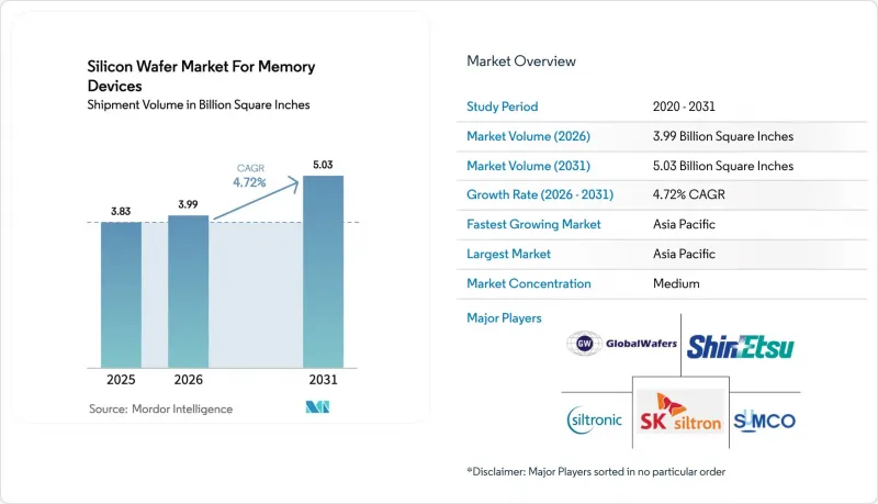
2025 年,用於儲存設備的矽晶圓市場價值為 38.3 億平方英寸,預計到 2031 年將達到 50.3 億平方英寸,而 2026 年為 39.9 億平方英寸,2026 年至 2031 年的年複合成長率(CAGR)為 4.72%成長率。
高頻寬記憶體的快速普及、向300毫米晶圓廠的轉型以及日益嚴格的汽車安全標準正在重新定義基板規格,而政府補貼則抵消了資本投資的周期性波動。對滿足混合鍵合平整度要求的高品質拋光晶圓的需求不斷成長,增強了一級供應商的議價能力,而專用SOI(絕緣薄膜矽)基板則在汽車雷達和5G射頻前端領域開闢了盈利的細分市場。美國《晶片與科學法案》和歐洲《晶片法案》推動的供應鏈區域化正在形成平行的晶圓生態系統,其中的競爭不再僅僅基於價格,而是以國家安全為中心。儘管基板供應商已將業務多元化拓展至先進封裝服務領域,但對能源效率法規的日益關注以及多晶矽價格的波動仍然是成本方面的阻力。
儲存裝置用矽晶圓市場趨勢與展望
加速向300毫米晶圓廠轉型
記憶體製造商正在逐步淘汰其 200 毫米生產線,轉而投資 300 毫米平台。 300 毫米平台可將每片晶圓的晶片面積提高 2.25 倍,並將每 GB 的基板成本降低約 30%。台積電熊本 Fab 2 工廠已獲得 300 毫米產能,用於生產汽車客戶的特殊 DRAM。同時,三星和 SK 海力士正在將其 200 毫米生產線改造為研發中心,以加速下一代材料的開發。用於 HBM3 E 的先進製程節點依賴穿透矽通孔(TSV),而 TSV 只有在 300 毫米基板才具有經濟可行性。中國大陸和台灣的中小型晶圓代工廠正在積極採用翻新的 300 毫米製造設備,以克服出口管制壁壘,擴大部署規模並滿足長期的基板需求。這一趨勢使得記憶體整合裝置製造商 (IDM) 能夠在相同直徑的基板上整合邏輯和 DRAM,這對於「記憶體運算」架構的效率至關重要。
人工智慧主導的資料中心記憶體需求正在不斷成長。
目前,人工智慧叢集正在使用HBM堆疊技術,與DDR5相比,每Terabyte所需的晶圓面積增加了40%。 SK海力士將於2025年第二季出貨12層HBM3 E,美光將於2026年初推出36GB堆疊,兩者均採用300mm基底晶圓,並帶有細間距銅柱凸塊。超大規模資料中心業者也在部署GDDR7用於推理工作負載,這形成了雙需求曲線,有利於那些能夠同時供應HBM超薄晶圓和GDDR7標準晶圓的供應商。 SEMI預測,到2027年,人工智慧相關的DRAM將佔DRAM晶圓總開工量的28%,是2024年的兩倍。隨著GPU記憶體佔用量的增加,即使DRAM價格下降,基板訂單依然強勁,從而緩解了晶圓供應商的營收波動。
透過記憶體IDM降低週期性資本支出
由於DRAM價格跌破成本,記憶體製造商在2024年至2025年間削減了120億美元的資本支出,推遲了新工廠的運作,並減少了晶圓採購。三星推遲了其平澤P4工廠的擴建計劃,美光也推遲了在愛達荷州和新加坡的設備部署。鑑於晶圓生產前置作業時間為12至18個月,訂單的突然取消會導致基板供應商庫存過剩,利潤率可能下降高達300個基點。雖然照付不議合約可以降低風險,但積體電路製造商(IDM)在景氣衰退時期往往會拒絕此類契約,從而導致市場波動持續。
細分市場分析
到2025年,用於儲存裝置的300mm矽晶片市場佔有率將佔總市場佔有率的85.73%(按銷量計),預計到2031年,該細分市場將以5.11%的複合年成長率成長。如此巨大的市場佔有率表明,用於儲存裝置的矽晶圓市場在直徑層面上規模龐大,促使供應商專注於超光滑拋光和低缺陷密度。 10nm以下DRAM節點的極紫外(EUV)光刻要求總厚度偏差控制在0.2µm以下,只有少數供應商能夠達到這一標準,從而設定了很高的准入門檻。通用200mm矽晶片在傳統汽車功率IC領域仍有需求,但其成長率僅2.8%,且隨著翻新300mm設備在中國和東南亞地區的普及,其需求已出現下滑跡象。小於 150 毫米的晶圓仍然屬於 MEMS 的小眾市場,但它們的總合佔有率不到 1.3%,這使得它們在戰略上與主流記憶體製造商無關。
就設備折舊而言,300mm生產線具有優勢,因為其每批次晶片的表面積是200mm生產線的2.25倍,而人事費用和公用設施成本並未成比例增加。台積電將其熊本第二工廠專門用於生產特種DRAM,這表明目前記憶體和邏輯晶片在高階300mm晶圓產能方面展開了激烈的競爭。因此,2025年簽訂的300mm晶圓長期合約價格上漲了8%至12%。由於新建工廠的成本超過5億美元,小規模的供應商選擇退出或成立合資企業。寡占企業正在利用規模經濟,並投資於TSV(矽通孔)相容基板,以確保未來在3D DRAM領域的發展機會。
《儲存裝置用矽晶圓市場報告》依晶圓直徑(150毫米及以下、200毫米、300毫米)、晶圓類型(拋光面、外延面、SOI(絕緣薄膜矽)、特種矽)、最終用戶(家用電子電器、工業、電信及其他)及地區(北美、歐洲、亞太地區及其他)進行細分。市場預測以體積(平方英吋)為單位。
區域分析
2025年,亞太地區將佔全球矽晶圓產量的83.19%,主導儲存裝置矽晶圓市場,預計到2031年將以5.16%的複合年成長率成長。韓國平澤和利川的垂直整合型工廠已將基板前置作業時間從18個月縮短至12個月,從而形成寶貴的良率回饋循環。台灣的矽晶圓生態系統受惠於台積電-SONY-電裝熊本合資企業,該合資企業利用日本政府提供的4,760億日圓(約32億美元)補貼,在台灣本地生產部分DRAM矽晶圓。中國在亞太地區18%的市佔率主要由上海新貴和GRINM等企業推動,但目前仍依賴進口多晶矽和晶體提取設備,出口限制可能對其造成衝擊。
在《晶片製造和整合法案》(CHIPS Act)津貼的支持下,北美預計到2025年將佔全球晶片產量的9%。 Global Wafers位於謝爾曼的工廠預計到2028年每年將生產120萬片300毫米晶圓,這將降低美國對進口的依賴。歐洲的市佔率為4%,但由於《晶片製造和整合法案》提供的430億歐元(約460億美元)的獎勵支持英飛凌和意法半導體的擴張,其增速略微放緩至4.3%。然而,供應鏈仍分散,規模經濟帶來的成本優勢有限,因為Siltronic的業務遍及德國和新加坡。南美洲、中東和非洲總合市場佔有率仍不足1%,由於本國沒有記憶體製造工廠,它們面臨巨額資本投資帶來的高進入門檻。
因此,儲存裝置用矽晶圓市場集中在三大製造地:東亞的巨型晶圓廠、北美的本土產能以及歐洲的中型專業生產線。儘管政策制定者正努力增強區域韌性,但由於原料集中且依賴製造設備,真正的自給自足預計還需要數年時間。對供應商而言,這種區域結構意味著他們需要在日益本地化的物流網路中,平衡多重合規系統並確保準時交貨。
其他好處:
- Excel格式的市場預測(ME)表
- 3個月的分析師支持
目錄
第1章:引言
- 研究假設和市場定義
- 調查範圍
第2章:調查方法
第3章執行摘要
第4章 市場狀況
- 市場概覽
- 產業價值鏈分析
- 技術分析
- 監理情勢
- 宏觀經濟因素對市場的影響
- 市場促進因素
- 加速向300毫米晶圓廠轉型
- 人工智慧主導的資料中心記憶體需求正在不斷成長。
- 擴展ADAS和EV平台的汽車記憶體
- 3D DRAM/NRAM堆疊的商業化
- 透過線上雷射退火提高晶圓良率。
- 政府晶片產業獎勵旨在促進國內晶圓生態系的發展
- 市場限制因素
- 透過記憶體IDM降低週期性資本支出
- 多晶矽原料供應瓶頸
- 能源密集型合規成本不斷增加
- 450mm刀具套裝認證延期
- 技術展望
- 波特五力分析
- 供應商的議價能力
- 買方的議價能力
- 新進入者的威脅
- 替代品的威脅
- 競爭公司之間的競爭
第5章 市場規模與成長預測
- 依晶圓直徑
- 最大可達 150 毫米
- 200 mm
- 300 mm
- 依晶片類型
- 拋光
- 外延
- 絕緣體上矽(SOI)
- 特種矽(高電阻、高功率、感測器級)
- 最終用戶
- 家用電子產品
- 手機和智慧型手機
- 個人電腦和伺服器
- 工業的
- 溝通
- 車
- 其他終端用戶應用程式
- 家用電子產品
- 按地區
- 北美洲
- 美國
- 加拿大
- 墨西哥
- 歐洲
- 德國
- 英國
- 法國
- 其他歐洲地區
- 亞太地區
- 中國
- 日本
- 印度
- 韓國
- 台灣
- 亞太其他地區
- 南美洲
- 中東和非洲
- 北美洲
第6章 競爭情勢
- 市場集中度
- 策略趨勢
- 市佔率分析
- 公司簡介
- Shin-Etsu Chemical Co., Ltd.
- SUMCO Corporation
- GlobalWafers Co., Ltd.
- Siltronic AG
- SK Siltron Co., Ltd.
- Soitec SA
- Okmetic Oy
- Wafer Works Corporation
- Zing Semiconductor Corporation
- Topsil Semiconductor Materials A/S
- Silicon Materials Inc.
- GCL-Advanced Material Co., Ltd.
- Shanghai Simgui Technology Co., Ltd.
- GRINM Semiconductor Materials Co., Ltd.
- Zhejiang Jinruihong(QL Electronics)
- Kinik Company
- Poshing Microelectronics Ltd.
- Win Win Precision Technology Co., Ltd.
- Nan Ya Photonics Inc.
第7章 市場機會與未來展望
The silicon wafer market for memory devices market size was valued at 3.83 billion square inches in 2025 and estimated to grow from 3.99 billion square inches in 2026 to reach 5.03 billion square inches by 2031, at a CAGR of 4.72% during 2026-2031.
Rapid adoption of high-bandwidth memory, migration to 300 mm fabs, and tighter automotive safety requirements are reshaping substrate specifications, while government subsidies counterbalance cyclical capital-expenditure swings. Rising demand for prime polished wafers that meet hybrid-bonding flatness targets is deepening the bargaining power of tier-one suppliers, yet specialty silicon-on-insulator (SOI) substrates are carving a profitable niche in automotive radar and 5 G RF front-ends. Regionalization of supply chains under the US CHIPS and Science Act and the European Chips Act is creating parallel wafer ecosystems that compete on sovereign security rather than just price. Intensifying focus on energy-intensity compliance and polysilicon price volatility remains a cost headwind for substrate vendors even as they diversify into advanced-packaging services.
Insights and Trends of Silicon Wafer Market For Memory Devices
Accelerating Transition to 300 mm Fabs
Memory manufacturers are decommissioning 200 mm lines and pouring capital into 300 mm platforms that generate 2.25X more die area per wafer, slicing per-gigabyte substrate cost by roughly 30%. TSMC's Kumamoto Fab 2 earmarks 300 mm capacity for specialty DRAM aimed at automotive clients, and Samsung plus SK Hynix are repurposing 200 mm facilities into R&D centers to speed next-generation materials work. Advanced nodes for HBM3 E rely on through-silicon vias that remain economical only on 300 mm substrates. Smaller foundries in China and Taiwan are snapping up refurbished 300 mm toolsets to leapfrog export-control hurdles, widening the installed base and underpinning long-term substrate demand. The trend also lets memory IDMs co-locate logic and DRAM on the same diameter, an efficiency play for compute-in-memory architectures.
Expansion of AI-Driven Memory Demand in Data Centers
Generative-AI clusters now absorb HBM stacks that need 40% more wafer area per terabyte than DDR5. SK hynix shipped 12-high HBM3 E in 2Q 2025 and Micron moved to 36 GB stacks in early 2026, both based on 300 mm base wafers featuring fine-pitch copper pillar bumps. Hyperscalers also roll out GDDR7 for inference workloads, creating a dual-track demand curve that rewards wafer vendors who can supply ultra-flat substrates for HBM alongside standard wafers for GDDR7. SEMI projects AI-tied DRAM will hit 28% of total DRAM wafer starts by 2027, double 2024 levels. As GPU memory footprints expand, substrate orders remain resilient even during DRAM pricing dips, cushioning revenue swings for wafer suppliers.
Cyclical Cap-Ex Cuts by Memory IDMs
Memory producers slashed capital expenditure by USD 12 billion in 2024-2025 amid sub-cash-cost DRAM pricing, postponing new fab ramps and throttling wafer procurement. Samsung deferred its Pyeongtaek P4 expansion, and Micron delayed equipment installs in Idaho and Singapore. Given a 12-18-month wafer production lead time, abrupt order cancellations saddle substrate vendors with excess inventory, eroding margins by up to 300 basis points. Take-or-pay contracts could mitigate risk, but IDMs resist during downturns, prolonging volatility.
Other drivers and restraints analyzed in the detailed report include:
- Growing Automotive Memory for ADAS and EV Platforms
- Commercialization of 3 D DRAM/NRAM Stacks
- Supply Bottlenecks in Polysilicon Feedstock
For complete list of drivers and restraints, kindly check the Table Of Contents.
Segment Analysis
The 300 mm slice of the silicon wafer market for memory devices commanded 85.73% volume in 2025, and the segment is set to grow at 5.11% CAGR through 2031. That dominance translates into a substantial silicon wafer market size for memory devices at the diameter level, reinforcing supplier focus on ultra-flat polishing and low defect densities. Extreme ultraviolet lithography for sub-10 nm DRAM nodes imposes a total-thickness variation of less than 0.2 µm, a bar that only a few vendors can meet, reinforcing barriers to entry. Commodity 200 mm wafers retain traction for legacy automotive power ICs, yet a mere 2.8% growth rate flags a sunset trajectory as refurbished 300 mm toolsets permeate China and Southeast Asia. Wafers under 150 mm persist in MEMS niches, but their combined share is less than 1.3%, rendering them strategically irrelevant for mainstream memory producers.
Equipment amortization favors 300 mm lines because a single lot delivers 2.25X the die surface area of 200 mm lines without proportionally higher labor or utility costs. TSMC's choice to dedicate Kumamoto Fab 2 to specialty DRAM shows memory is now vying head-to-head with logic for premium 300 mm capacity. As a result, long-term 300 mm wafer contracts signed in 2025 rose in price by 8-12%. Smaller suppliers either exit or form joint ventures given greenfield fabs cost upward of USD 500 million. Oligopolists leverage scale to invest in through-silicon via ready substrates, locking in future 3 D DRAM opportunities.
The Silicon Wafer Market for Memory Devices Report is Segmented by Wafer Diameter (Up To 150mm, 200mm, and 300mm), Wafer Type (Prime Polished, Epitaxial, Silicon-On-Insulator, and Specialty Silicon), End-User (Consumer Electronics, Industrial, Telecommunications, and More), and Geography (North America, Europe, Asia-Pacific, and More). The Market Forecasts are Provided in Terms of Volume (Square Inches).
Geography Analysis
Asia-Pacific dominated the silicon wafer market for memory devices with 83.19% production volume in 2025, growing at 5.16% CAGR to 2031. South Korea's vertically integrated complexes in Pyeongtaek and Icheon shave substrate lead times from 18 to 12 months, yielding valuable yield-feedback loops. Taiwan's ecosystem benefits from TSMC-Sony-Denso's Kumamoto venture, which channels Japanese subsidies worth JPY 476 billion (USD 3.2 billion) to localize DRAM wafers. China's 18% slice within Asia-Pacific, led by Shanghai Simgui and GRINM, is still reliant on imported polysilicon and crystal-pulling tools, keeping the door open for export-control disruptions.
North America accounted for 9% of 2025 volume, lifted by CHIPS Act grants. GlobalWafers' Sherman plant will add 1.2 million 300 mm wafers annually by 2028, reducing U.S. dependence on imports. Europe's 4% share inches ahead at a 4.3% pace thanks to EUR 43 billion (USD 46 billion) in Chips Act incentives supporting Infineon and STMicroelectronics expansions. Still, supply remains fragmented, with Siltronic spanning Germany and Singapore, limiting scale-related cost advantages. South America and the Middle East and Africa together remain below 1%, lacking indigenous memory fabs and facing steep capital-barrier hurdles.
The silicon wafer market for memory devices therefore clusters around three manufacturing zones, East Asia mega-fabs, North American sovereign capacity, and Europe's mid-scale specialty lines. Policymakers push for local resilience, but raw-material concentration and tooling dependencies mean genuine self-sufficiency is years away. For suppliers, this geography mix implies juggling multiple compliance regimes while ensuring just-in-time delivery over an increasingly regionalized logistics map.
- Shin-Etsu Chemical Co., Ltd.
- SUMCO Corporation
- GlobalWafers Co., Ltd.
- Siltronic AG
- SK Siltron Co., Ltd.
- Soitec SA
- Okmetic Oy
- Wafer Works Corporation
- Zing Semiconductor Corporation
- Topsil Semiconductor Materials A/S
- Silicon Materials Inc.
- GCL-Advanced Material Co., Ltd.
- Shanghai Simgui Technology Co., Ltd.
- GRINM Semiconductor Materials Co., Ltd.
- Zhejiang Jinruihong (QL Electronics)
- Kinik Company
- Poshing Microelectronics Ltd.
- Win Win Precision Technology Co., Ltd.
- Nan Ya Photonics Inc.
Additional Benefits:
- The market estimate (ME) sheet in Excel format
- 3 months of analyst support
TABLE OF CONTENTS
1 INTRODUCTION
- 1.1 Study Assumptions and Market Definition
- 1.2 Scope of the Study
2 RESEARCH METHODOLOGY
3 EXECUTIVE SUMMARY
4 MARKET LANDSCAPE
- 4.1 Market Overview
- 4.2 Industry Value Chain Analysis
- 4.3 Technology Analysis
- 4.4 Regulatory Landscape
- 4.5 Impact of Macroeconomic Factors on the Market
- 4.6 Market Drivers
- 4.6.1 Accelerating Transition to 300 mm Fabs
- 4.6.2 Expansion of AI-Driven Memory Demand in Data Centers
- 4.6.3 Growing Automotive Memory for ADAS and EV Platforms
- 4.6.4 Commercialization of 3D DRAM/NRAM Stacks
- 4.6.5 In-line Laser Anneal Boosting Wafer Yields
- 4.6.6 Government CHIPS Incentives for Local Wafer Ecosystems
- 4.7 Market Restraints
- 4.7.1 Cyclical Cap-Ex Cuts by Memory IDMs
- 4.7.2 Supply Bottlenecks in Polysilicon Feedstock
- 4.7.3 Escalating Energy-Intensity Compliance Costs
- 4.7.4 Delayed Qualification of 450 mm Toolsets
- 4.8 Technological Outlook
- 4.9 Porter's Five Forces Analysis
- 4.9.1 Bargaining Power of Suppliers
- 4.9.2 Bargaining Power of Buyers
- 4.9.3 Threat of New Entrants
- 4.9.4 Threat of Substitutes
- 4.9.5 Intensity of Competitive Rivalry
5 MARKET SIZE AND GROWTH FORECASTS (VOLUME)
- 5.1 By Wafer Diameter
- 5.1.1 Up to 150 mm
- 5.1.2 200 mm
- 5.1.3 300 mm
- 5.2 By Wafer Type
- 5.2.1 Prime Polished
- 5.2.2 Epitaxial
- 5.2.3 Silicon-on-Insulator (SOI)
- 5.2.4 Specialty Silicon (High-Resistivity, Power, Sensor-Grade)
- 5.3 By End-user
- 5.3.1 Consumer Electronics
- 5.3.1.1 Mobile and Smartphones
- 5.3.1.2 PCs and Servers
- 5.3.2 Industrial
- 5.3.3 Telecommunications
- 5.3.4 Automotive
- 5.3.5 Other End-user Applications
- 5.3.1 Consumer Electronics
- 5.4 By Geography
- 5.4.1 North America
- 5.4.1.1 United States
- 5.4.1.2 Canada
- 5.4.1.3 Mexico
- 5.4.2 Europe
- 5.4.2.1 Germany
- 5.4.2.2 United Kingdom
- 5.4.2.3 France
- 5.4.2.4 Rest of Europe
- 5.4.3 Asia-Pacific
- 5.4.3.1 China
- 5.4.3.2 Japan
- 5.4.3.3 India
- 5.4.3.4 South Korea
- 5.4.3.5 Taiwan
- 5.4.3.6 Rest of Asia-Pacific
- 5.4.4 South America
- 5.4.5 Middle East and Africa
- 5.4.1 North America
6 COMPETITIVE LANDSCAPE
- 6.1 Market Concentration
- 6.2 Strategic Moves
- 6.3 Market Share Analysis
- 6.4 Company Profiles (includes Global Level Overview, Market Level Overview, Core Segments, Financials as available, Strategic Information, Market Rank/Share, Products and Services, Recent Developments)
- 6.4.1 Shin-Etsu Chemical Co., Ltd.
- 6.4.2 SUMCO Corporation
- 6.4.3 GlobalWafers Co., Ltd.
- 6.4.4 Siltronic AG
- 6.4.5 SK Siltron Co., Ltd.
- 6.4.6 Soitec SA
- 6.4.7 Okmetic Oy
- 6.4.8 Wafer Works Corporation
- 6.4.9 Zing Semiconductor Corporation
- 6.4.10 Topsil Semiconductor Materials A/S
- 6.4.11 Silicon Materials Inc.
- 6.4.12 GCL-Advanced Material Co., Ltd.
- 6.4.13 Shanghai Simgui Technology Co., Ltd.
- 6.4.14 GRINM Semiconductor Materials Co., Ltd.
- 6.4.15 Zhejiang Jinruihong (QL Electronics)
- 6.4.16 Kinik Company
- 6.4.17 Poshing Microelectronics Ltd.
- 6.4.18 Win Win Precision Technology Co., Ltd.
- 6.4.19 Nan Ya Photonics Inc.
7 MARKET OPPORTUNITIES AND FUTURE OUTLOOK
- 7.1 White-Space and Unmet-Need Assessment

 數位記憶體增強平台市場預測(2034 年)—按平台類型、技術、應用、目標記憶體區域、最終用戶和地區分類的全球分析
 HBM4:市場佔有率分析、產業趨勢與統計、成長預測(2026-2031)LPDDR:市場佔有率分析、產業趨勢與統計、成長預測(2026-2031)邏輯裝置用矽晶圓:市場佔有率分析、產業趨勢與統計資料以及成長預測(2026-2031 年)記憶體處理單元 (MPU) 市場預測至 2034 年—按架構類型、記憶體技術、組件、應用、最終用戶和地區分類的全球分析
 2026年全球軍工和航太應用記憶體和處理器市場報告2026年全球儲存層級記憶體市場報告
 數位射頻記憶體市場:依產品類型、容量、應用和最終用戶分類-2026-2032年全球預測
 HBM全球市場預測(2026):AI主導的需求與HBM4生產趨勢
 數位射頻記憶體市場-全球產業規模、佔有率、趨勢、機會、預測:架構、應用、平台、區域及競爭格局(2021-2031年)