


 |
市場調查報告書
商品編碼
1911415
2.5D 和 3D 半導體封裝:市場佔有率分析、產業趨勢和統計數據、成長預測(2026-2031 年)2.5D And 3D Semiconductor Packaging - Market Share Analysis, Industry Trends & Statistics, Growth Forecasts (2026 - 2031) |
||||||
※ 本網頁內容可能與最新版本有所差異。詳細情況請與我們聯繫。
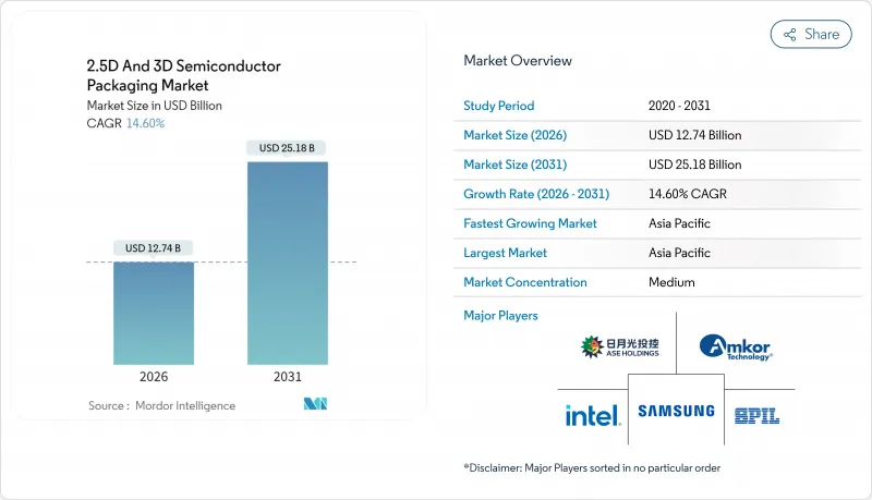
預計 2.5D 和 3D 半導體封裝市場將從 2025 年的 111.2 億美元成長到 2026 年的 127.4 億美元,到 2031 年將達到 251.8 億美元,2026 年至 2031 年的複合成長率為 14.6%。
在每秒Terabyte級頻寬需求的AI訓練叢集、汽車感測器融合平台以及空間受限的行動裝置的推動下,整個生態系統正在投資於中介層產能、晶片標準和高效散熱基板,以滿足不斷成長的需求。代工廠正在推進內部封裝以確保利潤率和藍圖控制,而OSAT(外包組裝和測試)公司則專注於為汽車和光電應用場景提供專用組裝。美國、歐洲和亞洲的政府補貼正在支持地域多角化,但矽中介層短缺和散熱限制制約了短期成長空間。隨著玻璃芯基板、混合鍵合和共封裝光學元件的日益普及,未來十年,封裝創新而非電晶體密度將決定系統性能。
全球2.5D及3D半導體封裝市場趨勢及洞察
AI/ML工作負載需要超高的記憶體頻寬
擁有超過兆個參數的超大規模學習模型正使傳統的DDR介面達到飽和,促使GPU廠商推廣邏輯封裝,從而實現每個插槽3TB/s的頻寬。穿透矽通孔(TSV)縮短了互連長度,降低了延遲,並支援相鄰記憶體操作,與分立式佈局相比,系統電力消耗降低了15%。 CoWoS和Foveros平台將記憶體和晶粒放置在共用的中介層上。這種拓樸結構也有利於邊緣推理設備,因為外形尺寸的限制使得它們無法採用分立式DIMM。三星和SK海力士的記憶體處理原型進一步模糊了邏輯和儲存之間的界限,證實了2.5D和3D半導體封裝市場是消除效能瓶頸的關鍵。資料中心營運商現在將機架能源效率指標與封裝記憶體頻寬直接掛鉤,將封裝決策轉化為超大規模擴展的資本支出槓桿。
智慧型手機和穿戴式裝置的微型化
高階智慧型手機將超過 50 種功能整合到系統級封裝)模組中,從而減少了 40% 的基板面積。扇出型晶圓層次電子構裝將 Z 軸高度降低至 0.5 毫米以下。智慧型手錶正在追求更高的密度,需要在小於 100 平方毫米的封裝內異構整合無線電、感測器和電源管理等功能。用於下一代穿戴式裝置的可拉伸電子元件對機械應變提出了更高的要求,而有機基板無法滿足這項要求,這推動了抗翹曲的 RDL 優先扇出製程的應用。穿戴式音訊設備和醫療設備日益普及,使得生物相容性封裝和防潮層成為必需,從而擴大了 2.5D 和 3D 半導體封裝在消費健康領域的市場佔有率。封裝級電磁干擾 (EMI) 屏蔽曾經是可選的,但現在已成為口袋大小設備中毫米波通訊和超寬頻測距的必備功能。
擴大對TSV/中介層製造設備的資本投資
專用CoWoS生產線的成本是標準組裝的3到4倍,每條生產線的總投資額高達100億美元。折舊免稅額期延長至10年,迫使OSAT製造商承擔高昂的固定成本,從而削弱了其價格競爭力。設備供應商的壟斷導致前置作業時間超過18個月,增加了供應鏈風險。小規模的組裝製造商無法資金籌措,因此正在退出高階2.5D和3D半導體封裝市場,並將資源集中到上游代工廠。
細分市場分析
到2025年,3D TSV解決方案將佔總收入的43.72%,維持14.85%的複合年成長率,使其在2.5D和3D半導體封裝市場佔有率競爭中處於領先地位。三星的HBM3E堆疊每個裝置可提供1.15TB/s的頻寬,與平面佈局相比,尺寸縮小了60%,基板電源軌減少了30%。
對人工智慧處理能力日益成長的需求推動了混合鍵合技術的發展,該技術無需微凸塊,並將互連間距縮小至10µm以下。台積電的SoIC樣品顯示互連密度提高了10倍,在高產量比率下幾乎可以媲美單晶片的效能。扇出晶圓層次電子構裝在行動電話領域仍然至關重要,在該領域,薄化比TSV更為重要;而基於中介層的2.5D橋接技術正逐漸成為晶片級CPU的主流。在預測期內,玻璃芯和背面饋電TSV技術的應用正在模糊不同封裝類型之間的界限,使混合模式封裝成為事實上的高階配置,並擴大2.5D和3D半導體封裝市場的整體規模。
區域分析
到2025年,亞太地區將佔總營收的60.05%,主要得益於台灣的CoWoS生產線和馬來西亞在全球後端生產中13%的佔有率。到2031年,越南和泰國為提升基板和測試產能而推出的激勵措施將推動亞太地區實現15.14%的複合年成長率。
北美地區借助 CHIPS 法案撥款加速發展:英特爾位於俄亥俄州的工廠和安姆科投資 20 億美元的亞利桑那州工廠將共同將區域處理能力提高 20%;國防封裝法規將把安全工作負載轉移到國內;SK 海力士計劃在堪薩斯州建設的工廠將擴大 HBM組裝,使其更靠近重要的雲資料中心客戶。
歐洲正著力發展汽車和工業可靠性領域,德國的「矽谷薩克森」(Silicon Saxony)和荷蘭的光子叢集( 光電 Cluster)都獲得了歐洲地平線基金的支持。儘管歐盟的市場佔有率落後於亞洲,但其在高可靠性領域的比例正在不斷提高,從而推動了該地區2.5D和3D半導體封裝市場的規模成長。雖然南美、中東和非洲等新興地區仍在進口成品封裝裝置,但它們正在吸引投資以實現最終測試的本地化,這反映出全球集中供應鏈風險的逐步分散。
其他福利:
- Excel格式的市場預測(ME)表
- 3個月的分析師支持
目錄
第1章 引言
- 研究假設和市場定義
- 調查範圍
第2章調查方法
第3章執行摘要
第4章 市場情勢
- 市場概覽
- 市場促進因素
- AI/ML工作負載需要超高的記憶體頻寬
- 智慧型手機和穿戴式裝置的微型化
- 推動汽車高階駕駛輔助系統的電氣化
- 玻璃芯基板向大量生產測試階段過渡
- 美國國防部強制要求國內3D-IC OSAT廠商使用安全晶片
- 晶片組設計的快速普及
- 市場限制
- TSV/中介層工廠資本支出增加
- 測試設計複雜性與產量比率損耗
- 全球矽錠短缺,無法滿足中介層需求
- 溫度控管和可靠性限制
- 產業價值鏈分析
- 監管環境
- 技術展望
- 波特五力分析
- 供應商的議價能力
- 買方的議價能力
- 新進入者的威脅
- 替代品的威脅
- 競爭對手之間的競爭
第5章 市場規模與成長預測
- 透過包裝技術
- 2.5D 中介層/光纖封裝
- 3D堆疊(TSV/混合鍵結)
- 晶圓級CSP
- 按最終用戶行業分類
- 家用電子電器
- 資料中心和高效能運算
- 通訊和電信
- 汽車和ADAS
- 醫療設備
- 工業和物聯網
- 其他終端用戶產業
- 透過使用
- 高效能邏輯晶片(CPU、GPU、AI加速器、ASIC、FPGA)
- 記憶體(HBM、DRAM 堆疊、3D NAND)
- 射頻和光電
- 混合訊號和感測器整合(ADC/DAC混合訊號積體電路、MEMS感測器、感測器集線器封裝)
- 按地區
- 北美洲
- 美國
- 加拿大
- 墨西哥
- 歐洲
- 德國
- 法國
- 英國
- 義大利
- 其他歐洲地區
- 亞太地區
- 中國
- 日本
- 韓國
- 印度
- 亞太其他地區
- 南美洲
- 巴西
- 阿根廷
- 南美洲其他地區
- 中東
- 以色列
- 沙烏地阿拉伯
- 阿拉伯聯合大公國
- 其他中東地區
- 非洲
- 南非
- 埃及
- 其他非洲地區
- 北美洲
第6章 競爭情勢
- 市場集中度
- 策略趨勢
- 供應商定位分析
- 公司簡介
- Advanced Semiconductor Engineering Inc.
- Amkor Technology Inc.
- Taiwan Semiconductor Manufacturing Company Limited
- Samsung Electronics Co., Ltd.
- Intel Corporation
- Siliconware Precision Industries Co., Ltd.
- Powertech Technology Inc.
- Jiangsu Changjiang Electronics Technology Co., Ltd.
- GlobalFoundries Inc.
- United Microelectronics Corporation
- Tezzaron Semiconductor Corporation
- STATS ChipPAC Pte. Ltd.
- TongFu Microelectronics Co., Ltd.
- Hana Micron Inc.
- Kulicke and Soffa Industries Inc.
第7章 市場機會與未來展望
The 2.5D and 3D semiconductor packaging market is expected to grow from USD 11.12 billion in 2025 to USD 12.74 billion in 2026 and is forecast to reach USD 25.18 billion by 2031 at 14.6% CAGR over 2026-2031.
Driven by AI training clusters that demand terabytes-per-second bandwidth, automotive sensor fusion platforms, and space-constrained mobile devices, the ecosystem is investing in interposer capacity, chiplet standards, and thermally efficient substrates to keep pace. Foundries have moved packaging in-house to secure margins and roadmap control, while OSATs double down on specialty assembly for automotive and photonics use cases. Government subsidies in the United States, Europe, and Asia support regional diversification, yet silicon interposer shortages and cooling limits temper near-term upside. As glass-core substrates, hybrid bonding, and co-packaged optics move toward mass adoption, packaging innovation-not transistor density-will define the next decade of system performance.
Global 2.5D And 3D Semiconductor Packaging Market Trends and Insights
AI/ML Workloads Demanding Ultra-High Memory Bandwidth
Hyperscale training models that now exceed 1 trillion parameters saturate traditional DDR interfaces, prompting GPU vendors to co-package logic with HBM3 stacks delivering 3 TB/s bandwidth-per-socket . Through-silicon vias shorten trace lengths and cut latency, enabling near-memory compute that lowers system power budgets by 15% versus discrete layouts. CoWoS and Foveros platforms position memory and accelerator dies on a shared interposer, a topology that also benefits edge inference devices where form factors prohibit discrete DIMMs. Processing-in-memory prototypes from Samsung and SK Hynix further blur boundaries between logic and storage, reinforcing the 2.5D and 3D semiconductor packaging market as a performance bottleneck eliminator. Data-center operators now tie rack energy efficiency metrics directly to packaged memory bandwidth, converting packaging decisions into capital-expense levers for hyperscale expansions.
Smartphone and Wearable Miniaturization
Premium smartphones integrate more than 50 functions inside system-in-package modules, shrinking board footprint by 40% and cutting z-height below 0.5 mm through fan-out wafer-level packaging . Smartwatches push density further, demanding heterogeneous integration of radios, sensors, and power management in packages under 100 mm2. Stretchable electronics for next-gen wearables add mechanical-strain constraints that organic substrates cannot meet, spurring adoption of warpage-resistant RDL-first fan-out processes. Biocompatible encapsulants and moisture barriers become mandatory as hearables and medical wearables proliferate, enlarging the 2.5D and 3D semiconductor packaging market addressable share within consumer health. Package-level EMI shielding, once optional, is now table stakes for millimeter-wave connectivity and ultra-wideband ranging inside pocket-sized devices.
Escalating CapEx for TSV/Interposer Fabs
Individual CoWoS lines cost 3-4 times standard assembly capacity and push total investment toward USD 10 billion per site . Depreciation periods elongate to 10 years, locking OSATs into high fixed costs that erode price agility. Equipment vendor oligopolies raise tool lead-times beyond 18 months, heightening supply-chain risk. Smaller assemblers, unable to finance TSV etch modules or hybrid-bond aligners, exit the high-end 2.5D and 3D semiconductor packaging market, concentrating power upstream at foundries.
Other drivers and restraints analyzed in the detailed report include:
- Automotive ADAS Electrification Push
- Glass-Core Substrates Entering Volume Trials
- Design-for-Test Complexity and Yield Loss
For complete list of drivers and restraints, kindly check the Table Of Contents.
Segment Analysis
3D TSV solutions captured 43.72% of 2025 revenue, and their 14.85% CAGR keeps them at the forefront of the 2.5D and 3D semiconductor packaging market share race. Samsung's HBM3E stacks supply 1.15 TB/s bandwidth per device, shrinking footprint 60% and cutting board power rails by 30% over planar layouts .
Demand for AI throughput encourages hybrid bonding that eliminates micro-bumps and pushes interconnect pitch below 10 µm. TSMC SoIC samples show 10X interconnect density gains that nearly equal monolithic reticle performance at higher yields. Fan-out wafer-level packaging stays relevant in handsets where thinness outranks TSV, while interposer-based 2.5D bridges dominate chiplet CPUs. Over the forecast, glass-core adoption and backside-power TSVs will blur categorical lines, establishing mixed-mode packages as the de facto high-end configuration, enlarging the overall 2.5D and 3D semiconductor packaging market size.
The 2. 5D and 3D Semiconductor Packaging Market Report is Segmented by Packaging Technology (2. 5D Interposer/FO-SoW, 3D Stacked TSV/Hybrid Bond, and More), End-User Industry (Consumer Electronics, Data Centre and HPC, Communications and Telecom, and More), Application (High-Performance Logic, Memory, RF and Photonics, Mixed-Signal and Sensor Integration), and Geography. The Market Forecasts are Provided in Terms of Value (USD).
Geography Analysis
Asia Pacific commanded 60.05% of 2025 revenue, driven by Taiwan's CoWoS lines and Malaysia's 13% share of global back-end output . Ongoing 15.14% CAGR through 2031 arises from Vietnamese and Thai incentives that add substrate and test capacity.
North America accelerates on the back of CHIPS Act subsidies: Intel's Ohio complex and Amkor's USD 2 billion Arizona plant together raise local throughput by 20% . Defense packaging mandates concentrate secure workloads stateside, and SK Hynix's planned Kansas facility expands HBM-logic assembly near key cloud data-center customers.
Europe focuses on automotive and industrial reliability, with Germany's Silicon Saxony and the Netherlands' photonics clusters receiving Horizon Europe funds. While share lags Asia, EU content rises in high-reliability sectors, lifting the regional 2.5D and 3D semiconductor packaging market size. Emerging regions, South America, the Middle East, and Africa, import fully packaged devices but court investment to localize final test, reflecting a gradual de-risking of globally concentrated supply chains.
- Advanced Semiconductor Engineering Inc.
- Amkor Technology Inc.
- Taiwan Semiconductor Manufacturing Company Limited
- Samsung Electronics Co., Ltd.
- Intel Corporation
- Siliconware Precision Industries Co., Ltd.
- Powertech Technology Inc.
- Jiangsu Changjiang Electronics Technology Co., Ltd.
- GlobalFoundries Inc.
- United Microelectronics Corporation
- Tezzaron Semiconductor Corporation
- STATS ChipPAC Pte. Ltd.
- TongFu Microelectronics Co., Ltd.
- Hana Micron Inc.
- Kulicke and Soffa Industries Inc.
Additional Benefits:
- The market estimate (ME) sheet in Excel format
- 3 months of analyst support
TABLE OF CONTENTS
1 INTRODUCTION
- 1.1 Study Assumptions and Market Definition
- 1.2 Scope of the Study
2 RESEARCH METHODOLOGY
3 EXECUTIVE SUMMARY
4 MARKET LANDSCAPE
- 4.1 Market Overview
- 4.2 Market Drivers
- 4.2.1 AI/ML workloads demanding ultra-high memory bandwidth
- 4.2.2 Smartphone and wearable miniaturisation
- 4.2.3 Automotive ADAS electrification push
- 4.2.4 Glass-core substrates entering volume trials
- 4.2.5 U.S. DoD secure-chip mandates for on-shore 3D-IC OSATs
- 4.2.6 Rapid Uptake of Chiplet Designes
- 4.3 Market Restraints
- 4.3.1 Escalating CapEx for TSV/interposer fabs
- 4.3.2 Design-for-test complexity and yield loss
- 4.3.3 Global interposer silicon-ingot shortage issue
- 4.3.4 Thermal-management and reliability limits
- 4.4 Industry Value-Chain Analysis
- 4.5 Regulatory Landscape
- 4.6 Technological Outlook
- 4.7 Porters Five Forces Analysis
- 4.7.1 Bargaining Power of Suppliers
- 4.7.2 Bargaining Power of Buyers
- 4.7.3 Threat of New Entrants
- 4.7.4 Threat of Substitutes
- 4.7.5 Intensity of Competitive Rivalry
5 MARKET SIZE AND GROWTH FORECASTS (VALUE)
- 5.1 By Packaging Technology
- 5.1.1 2.5D Interposer / FO-SoW (includes CoWoS, EMIB, InFO-SoW, other interposer/fan-out-on-substrate)
- 5.1.2 3D Stacked (TSV / hybrid bond) (includes SoIC, Foveros, stacked DRAM like HBM)
- 5.1.3 Wafer-Level CSP
- 5.2 By End-User Industry
- 5.2.1 Consumer Electronics
- 5.2.2 Data Centre and HPC
- 5.2.3 Communications and Telecom
- 5.2.4 Automotive and ADAS
- 5.2.5 Medical Devices
- 5.2.6 Industrial and IoT
- 5.2.7 Other End-user Industries
- 5.3 By Application
- 5.3.1 High-Performance Logic(CPUs, GPUs, AI accelerators, ASICs, FPGAs)
- 5.3.2 Memory (HBM, DRAM stacks, 3D NAND)
- 5.3.3 RF and Photonics
- 5.3.4 Mixed-Signal and Sensor Integration (ADC/DAC mixed-signal ICs, MEMS sensors, sensor-hub packages)
- 5.4 By Geography
- 5.4.1 North America
- 5.4.1.1 United States
- 5.4.1.2 Canada
- 5.4.1.3 Mexico
- 5.4.2 Europe
- 5.4.2.1 Germany
- 5.4.2.2 France
- 5.4.2.3 United Kingdom
- 5.4.2.4 Italy
- 5.4.2.5 Rest of Europe
- 5.4.3 Asia Pacific
- 5.4.3.1 China
- 5.4.3.2 Japan
- 5.4.3.3 South Korea
- 5.4.3.4 India
- 5.4.3.5 Rest of Asia Pacific
- 5.4.4 South America
- 5.4.4.1 Brazil
- 5.4.4.2 Argentina
- 5.4.4.3 Rest of South America
- 5.4.5 Middle East
- 5.4.5.1 Israel
- 5.4.5.2 Saudi Arabia
- 5.4.5.3 United Arab Emirates
- 5.4.5.4 Rest of Middle East
- 5.4.6 Africa
- 5.4.6.1 South Africa
- 5.4.6.2 Egypt
- 5.4.6.3 Rest of Africa
- 5.4.1 North America
6 COMPETITIVE LANDSCAPE
- 6.1 Market Concentration
- 6.2 Strategic Moves
- 6.3 Vendor Positioning Analysis
- 6.4 Company Profiles (includes Global level Overview, Market level overview, Core Segments, Financials as available, Strategic Information, Products and Services, and Recent Developments)
- 6.4.1 Advanced Semiconductor Engineering Inc.
- 6.4.2 Amkor Technology Inc.
- 6.4.3 Taiwan Semiconductor Manufacturing Company Limited
- 6.4.4 Samsung Electronics Co., Ltd.
- 6.4.5 Intel Corporation
- 6.4.6 Siliconware Precision Industries Co., Ltd.
- 6.4.7 Powertech Technology Inc.
- 6.4.8 Jiangsu Changjiang Electronics Technology Co., Ltd.
- 6.4.9 GlobalFoundries Inc.
- 6.4.10 United Microelectronics Corporation
- 6.4.11 Tezzaron Semiconductor Corporation
- 6.4.12 STATS ChipPAC Pte. Ltd.
- 6.4.13 TongFu Microelectronics Co., Ltd.
- 6.4.14 Hana Micron Inc.
- 6.4.15 Kulicke and Soffa Industries Inc.
7 MARKET OPPORTUNITIES AND FUTURE OUTLOOK
- 7.1 White-space and Unmet-Need Assessment
 2026年全球半導體封裝市場報告
 3-D TSV:關鍵問題洞察與市場分析
 高密度封裝(MCM、MCP、SIP、3D-TSV):市場分析與技術趨勢
 全球防靜電載帶捲市場(按載帶類型、材料、膠帶材料成分、膠帶層數和最終用途產業分類)預測(2026-2032年)導線架固定膠帶市場(按黏合劑類型、背襯材料、膠頻寬度、膠帶厚度、應用、最終用途行業和銷售管道),全球預測,2026-2032年
 MEMS封裝焊料市場規模、佔有率和成長分析:按焊料類型、產品形式、應用、封裝類型、最終用戶和地區分類 - 2026-2033年產業預測
 先進半導體封裝市場分析及預測(至2035年):依類型、產品類型、服務、技術、應用、材料類型、裝置、製程、最終用戶及功能分類半導體原型製作及封裝市場分析及預測(至2035年):依類型、產品類型、服務、技術、應用、材料類型、組件、製程、最終用戶、設備分類半導體封裝市場分析及預測(至2035年):依類型、產品類型、技術、應用、材料類型、裝置、製程、最終用戶、功能、設備分類
 高階半導體封裝:市場佔有率分析、產業趨勢與統計、成長預測(2026-2031)