


 |
市場調查報告書
商品編碼
1940553
先進積體電路基板:市場佔有率分析、產業趨勢與統計、成長預測(2026-2031)Advanced IC Substrates - Market Share Analysis, Industry Trends & Statistics, Growth Forecasts (2026 - 2031) |
||||||
※ 本網頁內容可能與最新版本有所差異。詳細情況請與我們聯繫。
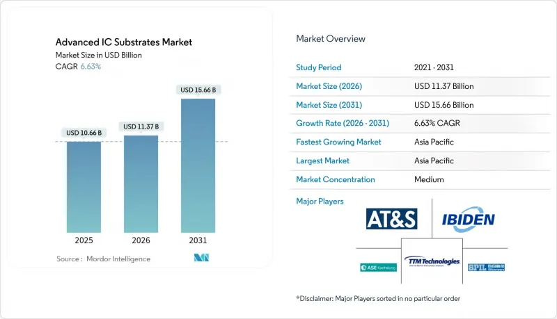
預計先進積體電路基板市場將從 2025 年的 106.6 億美元成長到 2026 年的 113.7 億美元,到 2031 年將達到 156.6 億美元,2026 年至 2031 年的複合年成長率為 6.63%。
市場需求已從傳統運算轉向以人工智慧為中心的工作負載,這需要更高的層數、更細的線寬和更嚴格的翹曲控制。亞太地區的基板供應商受益於此轉變,因為他們已經擁有強大的ABF產能,並與代工廠的封裝生產線建立了緊密的合作關係。主要雲端服務供應商將長期採購協議的期限提前至2025年,以確保CoWoS和FC-BGA的穩定供應,這進一步增強了基板製造商的定價權。同時,玻璃芯技術的發展日益成熟,為超高密度封裝提供了一種替代ABF的策略選擇,預計將在2020年代末期實現商業化。
全球先進積體電路基板市場趨勢與洞察
AI/HPC加速器對ABF基板的需求快速成長
2025 代 AI 伺服器的大規模部署導致味之素積層製造膜 (ABF) 供應緊張。 ABF 面板的前置作業時間已超過 35 週,現貨價格較 2024 年合約價格溢價高達 25%。台灣供應商 Unimicron、Kinsus 和南亞 PCB 在經歷了長期的庫存調整後,營收已恢復兩位數成長,但為滿足需求,其運轉率仍維持在 90%。三星馬達在 2025 年第二季提高了其 AI 伺服器的 ABF 產能,並開始試生產玻璃芯。這體現了其為降低單一材料風險而採取的雙源策略。台積電已宣布計劃將 CoWoS 的年產量加倍,這意味著基板需求將顯著超過現有產能。這些發展已使供不應求擴大至 20%,基板製造商預計這種短缺狀況將持續到 2026 年新生產線運作為止。
幾何縮放和異質整合的趨勢
晶片組架構、無芯中介層和穿透矽通孔(TSV) 技術重新定義了封裝設計規則,使生產環境中的基板線寬低於 10µm。應用材料公司強調,與單晶粒方案相比,封裝內整合離散晶片組可實現更高的每瓦性能。凸版印刷推出了一種無芯有機中介層,其熱膨脹係數比傳統的 ABF 解決方案低 45%,從而降低了多晶片堆疊中的機械應力。博通公司的 3.5D XDSiP 技術將超過 6000mm² 的矽晶圓整合到 12 層 HBM 堆疊中,凸顯了對能夠在有限面積內佈線數千個高速訊號的基板的需求。台積電和日月光投資建造了尺寸高達 310x310mm 的面板級封裝生產線,以提高步進馬達效率並降低每平方英吋成本。這些變化正將先進 IC基板市場定位為實現下一代運算密度的關鍵基礎技術。
ABF基板供不應求和前置作業時間突然延長
從2024年到2025年,ABF面板持續的供不應求阻礙了先進IC基板市場的發展。 ABF樹脂的近乎壟斷供應商味之素株式會社承認,在新的樹脂反應器於2026年運作之前,供需缺口將達到20%。台積電表示其只能滿足CoWoS需求的80%,證實了代工廠面臨的限制。積水化學等競爭對手試圖擺脫對積層製造的依賴,但高階AI封裝的認證週期延緩了他們的實施。同時,因其低膨脹係數而備受青睞的T-Glass芯材的短缺,延緩了日東紡的產能擴張,並加劇了前置作業時間的延長。儘管基板製造商實施了在線連續計量以提高一次產量比率並最佳化現有產能,但大多數客戶在2025年之前仍需遵守配額計畫。
細分市場分析
到2025年,FC-BGA基板佔據了先進IC基板市場44.32%的佔有率。其主導地位源自於其久經考驗的電氣性能,而這正是AI加速器和伺服器CPU所必需的。由於GPU製造商競相確保產能,FC - BGA基板的運轉率在2025年全年保持高位。然而,成長重心轉向了用於汽車網域控制器和折疊式行動裝置的剛撓性CSP生產線。軟硬複合CSP的出貨量以7.94%的複合年成長率成長,吸引了能夠平衡彎曲半徑和可控電阻的新型基板供應商。 FC-CSP繼續為中階行動處理器提供基板,但成本壓力限制了平均售價的成長。有機BGA/LGA對於傳統桌面平台仍然很重要,但其設計應用逐漸被覆晶技術所取代。面板級FC基板(歸類為「其他」)已在台積電和日月光開始試生產,實現了單面板七倍的可用面積,並釋放了新的規模經濟效益。
FC-BGA 已成為 CoWoS 堆疊的主要基板。設計人員對 14-26 層電路板的需求日益成長,並對對準公差提出了更高的要求。為此, 基板製造商採用了人工智慧光學檢測設備,以便在堆疊初期階段即可偵測出過孔和走線的錯位。隨著汽車製造商將資訊娛樂系統升級到 15 吋曲面顯示器(需要 Z 軸方向的柔軟性),對軟硬複合CSP 的需求也隨之成長。折疊式設備中攝影機整合度的提高也帶來了額外的需求。預計到 2031 年,這些趨勢將使軟硬複合基板的市場滲透率持續保持成長,而 FC-BGA 將繼續在先進 IC基板市場中保持其高價值地位。
截至2025年,ABF(鋁基複合材料)佔據了先進IC基板市場60.35%的佔有率。味之素株式會社的專有樹脂配方技術確保了穩定的介電性能和可鑽孔性,贏得了客戶在2.5D和3D堆疊方面的信賴。儘管供應商在2025年擴大了ABF混合生產線,但產量成長卻落後於需求,從而鞏固了賣方優勢。玻璃基板在2025年的出貨量佔比不到2%,預計複合年成長率(CAGR)為13.58%。玻璃基板在200 mm x 200 mm的基板上實現了±5 μm的平整度,與ABF相比,能夠實現更精細的線路重布和更高的I/O密度。英特爾退出內部研發驗證了第三方玻璃供應商的可靠性,加速了生態系統的發展。
在汽車控制單元中,BT樹脂仍發揮效用,因為基板溫度通常高達150°C。陶瓷和低溫共燒陶瓷(LTCC)基板為承受持續熱循環的功率元件提供基板,在ABF生產線超賣時,它們能夠提供一定的收入緩衝。玻璃基板的認證在通孔形成均勻性方面遇到了一些挑戰,但最初的原型產品在回流焊接過程中展現了良好的抗翹曲特性。 AMD計畫在2026年CPU平台上使用玻璃化材料,促使基板製造商爭相在量產開始前鎖定生產名額。如果產量比率保持穩定,到2031年,玻璃基板的收入佔有率可能會達到或超過5.3%。
先進 IC基板市場按基板類型(FC-BGA、FC-CSP、有機 BGA/LGA 等)、核心材料(ABF、BT、玻璃等)、封裝技術(2D覆晶、2.5D 中介層等)、裝置節點(28nm 及以上、16/14-10nm 等)、終端用戶(A)、終端用戶、北美區域
區域分析
到2025年,亞太地區將佔據先進積體電路基板市場68.35%的佔有率。台灣的優尼美光、金碩和南亞PCB在人工智慧伺服器需求的推動下,於2025年實現了兩位數的成長,彌補了2023年因庫存調整而導致的出貨量下滑。在日本,台積電位於熊本的工廠憑藉3.9兆日圓(約255億美元)的補貼,重新確立了其在九州的封裝中心地位。韓國宣布了一項4,710億美元的綜合叢集計劃,目標是到2030年實現每月770萬片晶圓的開工量,併計劃在其邏輯晶片工廠附近建設一條ABF-CoWoS生產線。中國推出了區域性激勵措施以擴大覆晶和系統級封裝(SiP)產能,但出口限制制約了製造設備的採購,並減緩了玻璃芯的普及。
在北美,基於《晶片封裝法案》(CHIPS Act)的先進在地化正在推進。台積電位於亞利桑那州的園區正計劃建造六家工廠,並配備ABF生產線以分散風險。 Entegris公司已獲得高達7,500萬美元的聯邦援助,用於基板銅電鍍過濾介質的生產。一家大型OSAT公司正考慮拓展美國市場,以滿足國防工業對晶片封裝的需求,但不斷上漲的薪資水準令人擔憂。
歐洲正聚焦汽車和功率元件領域。安森美半導體位於捷克的碳化矽工廠正在該地區建立一條完整的逆變器基板供應鏈。德國和法國正考慮建立一條聯合ABF(先進基板)試點生產線,以支援英特爾和台積電的晶圓代工業務擴張。與此同時,越南、印度和馬來西亞正在推行組裝補貼計畫。安姆科在北寧省開設了一家價值16億美元的工廠,印度政府核准了760億盧比(約9.1億美元)的OSAT(外包半導體組裝和測試)業務投資,該業務由CG Power和瑞薩電子主導。這些發展進一步分散了先進積體電路基板市場的地理風險。
其他福利:
- Excel格式的市場預測(ME)表
- 3個月的分析師支持
目錄
第1章 引言
- 研究假設和市場定義
- 調查範圍
第2章調查方法
第3章執行摘要
第4章 市場情勢
- 市場概覽
- 市場促進因素
- AI/HPC加速器對ABF基板的需求快速成長
- 小型化和異質整合趨勢
- 5G基礎設施發展帶動了高頻射頻封裝的需求成長。
- 汽車和電動車的電氣化需要高度可靠的基板
- 玻璃芯基板允許的層數增加一倍以上。
- CHIPS補貼與基板製造廠掛鉤
- 市場限制
- ABF基板供不應求和前置作業時間突然延長
- 高資本密集度與流程複雜性
- 覆銅層壓板價格波動
- 加強對複合薄膜化學物質排放的監管
- 價值鏈分析
- 監管環境
- 技術展望
- 波特五力分析
- 供應商的議價能力
- 消費者議價能力
- 新進入者的威脅
- 替代品的威脅
- 競爭對手之間的競爭
- 定價分析
- 宏觀經濟因素的影響
第5章 市場規模與成長預測
- 依基材類型
- FC-BGA
- FC-CSP
- 有機BGA/LGA
- 軟硬複合和軟性CSP
- 其他
- 依核心材料
- ABF
- BT
- 玻璃
- LTCC/HTCC
- 陶瓷製品
- 透過包裝技術
- 2D覆晶
- 2.5D 中介層
- 3D-IC/SoIC
- 扇出WLP
- SiP/模組
- 按裝置節點(nm)
- 28奈米或更大
- 16/14-10 nm
- 7-5 nm
- 4奈米或更小
- 按最終用途行業分類
- 行動和消費者
- 汽車和運輸設備
- 資訊科技和通訊基礎設施
- 資料中心/人工智慧和高效能運算
- 工業、醫療及其他
- 按地區
- 北美洲
- 美國
- 加拿大
- 南美洲
- 巴西
- 南美洲其他地區
- 歐洲
- 德國
- 法國
- 英國
- 義大利
- 西班牙
- 俄羅斯
- 其他歐洲地區
- 亞太地區
- 中國
- 日本
- 韓國
- 台灣
- 印度
- 亞太其他地區
- 中東和非洲
- 中東
- 沙烏地阿拉伯
- 阿拉伯聯合大公國
- 土耳其
- 其他中東地區
- 非洲
- 南非
- 奈及利亞
- 其他非洲地區
- 中東
- 北美洲
第6章 競爭情勢
- 市場集中度
- 策略趨勢
- 市佔率分析
- 公司簡介
- ASE Technology Holding Co., Ltd.
- AT&S Austria Technologie & Systemtechnik AG
- Siliconware Precision Industries Co., Ltd.
- TTM Technologies, Inc.
- Ibiden Co., Ltd.
- Kyocera Corporation
- Fujitsu Interconnect Technologies Ltd.
- JCET Group Co., Ltd.
- Panasonic Holdings Corporation
- Kinsus Interconnect Technology Corp.
- Unimicron Technology Corp.
- Nan Ya Printed Circuit Board Corp.
- Samsung Electro-Mechanics Co., Ltd.
- LG Innotek Co., Ltd.
- Simmtech Co., Ltd.
- Shinko Electric Industries Co., Ltd.
- Shennan Circuits Co., Ltd.
- Zhen Ding Technology Holding Ltd.
- Daeduck Electronics Co., Ltd.
- Meiko Electronics Co., Ltd.
- WUS Printed Circuit Co., Ltd.
- Zhejiang Kingdom Sci-Tech Co., Ltd.
- SKC Absolics Inc.
- Tripod Technology Corp.
- Toppan Inc.
第7章 市場機會與未來展望
The advanced IC substrates market is expected to grow from USD 10.66 billion in 2025 to USD 11.37 billion in 2026 and is forecast to reach USD 15.66 billion by 2031 at 6.63% CAGR over 2026-2031.
Demand shifted decisively from traditional computing toward AI-centric workloads that require higher layer counts, finer linewidths, and tighter warpage control. Asia-Pacific-based substrate vendors benefited from this pivot because they already possessed high-volume ABF capacity and close relationships with foundry packaging lines. Major cloud service providers accelerated long-term purchase agreements in 2025 to secure guaranteed CoWoS and FC-BGA supply, further tilting pricing power to substrate producers. At the same time, glass-core innovation matured, creating a strategic alternative to ABF for ultra-high-density packages scheduled for commercial release in the latter half of the decade.
Global Advanced IC Substrates Market Trends and Insights
Surge in ABF-substrate demand for AI/HPC accelerators
Massive roll-outs of generative-AI servers in 2025 tightened supplies of Ajinomoto Build-up Film, pushing lead-times for ABF panels past 35 weeks and triggering spot-price premiums of up to 25% over 2024 contract levels. Taiwanese suppliers Unimicron, Kinsus, and Nan Ya PCB restored double-digit revenue growth after concluding a prolonged inventory correction, yet still operated at 90% utilization to keep pace with demand. Samsung Electro-Mechanics ramped AI-oriented ABF volume in Q2 2025 and started pilot glass-core runs, reflecting a dual-sourcing strategy aimed at mitigating single-material risk. TSMC disclosed plans to double annual CoWoS output, implying substrate demand well above existing capacity. Collectively, these moves widened a 20% supply gap that substrate makers do not expect to close until fresh lines come online in 2026.
Miniaturization and heterogeneous integration trend
Chiplet architectures, coreless interposers, and through-silicon vias redefined package design rules and pushed substrate line-widths below 10 µm in production settings. Applied Materials highlighted that on-package integration of discrete chiplets delivered superior performance per watt compared with monolithic die approaches. TOPPAN unveiled a coreless organic interposer with a 45% lower coefficient of thermal expansion than legacy ABF solutions, easing mechanical stress inside multi-die stacks. Broadcom's 3.5D XDSiP technology integrated more than 6,000 mm2 of silicon and 12 HBM stacks, underscoring the demand for substrates that can route thousands of high-speed signals in confined footprints. TSMC and ASE invested in panel-level packaging lines up to 310 X 310 mm to gain stepper efficiency and reduce cost per square inch. These shifts position the advanced IC substrates market as a pivotal enabler for next-generation compute density.
ABF-substrate capacity shortage and lead-time spikes
A persistent deficit in ABF panel output restricted upside for the advanced IC substrates market during 2024-2025. Ajinomoto, the near-monopoly supplier of ABF resin, acknowledged a 20% demand-supply gap that would remain until new resin reactors started in 2026. Foundries confirmed the constraint when TSMC said it could satisfy only 80% of CoWoS demand. Competitors such as Sekisui Chemical aimed to break dependence on alternate build-up chemistries, yet qualification cycles for high-end AI packages slowed adoption. Parallel shortages of T-Glass core material, prized for low expansion coefficients, delayed capacity expansions at Nittobo, compounding lead-time spikes. Substrate makers deployed inline metrology to raise first-pass yield and stretch existing capacity, but most customers still entered allocation programs through 2025.
Other drivers and restraints analyzed in the detailed report include:
- 5G build-out boosting high-frequency RF packaging
- Automotive-EV electrification needs high-reliability substrates
- High capital intensity and process complexity
For complete list of drivers and restraints, kindly check the Table Of Contents.
Segment Analysis
FC-BGA substrates accounted for 44.32% of the advanced IC substrates market share in 2025. Their lead is derived from proven electrical performance required by AI accelerators and server CPUs. Utilization stayed high through 2025 as GPU makers rushed to secure capacity. Growth, however, shifted toward rigid-flex CSP lines that served automotive domain controllers and foldable mobile devices. Rigid-flex volume increased at an 7.94% CAGR, attracting new laminate suppliers able to balance bend radius with controlled impedance. FC-CSP continued to service mid-tier mobile processors, but its cost pressures limited ASP upside. Organic BGA/LGA remained relevant for legacy desktop platforms, yet ceded design wins to flip-chip options. Panel-level FC substrates, still counted under "Others," emerged in pilot volumes at TSMC and ASE, promising 7X usable area per panel and opening new economies of scale.
FC-BGA stayed the workhorse for CoWoS build-ups. Designers demanded 14-26 layer counts, forcing tighter registration tolerances. In response, substrate makers installed AI-enabled optical inspection to catch via-to-trace violations early in the stack. Rigid-flex CSP benefited when automakers migrated infotainment units to 15-inch curved displays that required Z-axis flexibility. Increased camera integration in foldables presented an additional pull. These dynamics support sustained penetration for rigid-flex through 2031 while FC-BGA continues to anchor high-value positions within the advanced IC substrates market.
ABF represented 60.35% of the advanced IC substrates market size in 2025. Ajinomoto's exclusive resin recipe established consistent dielectric performance and drillability that customers trusted for 2.5D and 3D stacks. Suppliers expanded ABF mixing rooms in 2025, but output gains lagged demand growth, reinforcing seller leverage. Glass substrates, though less than 2% of 2025 shipments, recorded a 13.58% forecast CAGR. Flatness within +-5 µm across 200 mm x 200 mm plates allowed finer redistribution layers and higher I/O density than ABF. Intel's exit from in-house development validated third-party glass suppliers and accelerated ecosystem readiness.
BT resin preserved relevance in automotive control units where 150 °C board temperatures were common. Ceramic and LTCC segments supplied power devices exposed to continuous thermal cycling and offered incremental revenue buffers when ABF lines were oversold. Qualification of glass cores faced hurdles in via formation uniformity, but early builds delivered promising warpage metrics at reflow. AMD signaled its intention to switch its 2026 CPU platforms to glass, encouraging substrate makers to lock capacity slots well ahead of volume ramps. If yields hold, glass could equal or surpass 5.3% revenue share by 2031.
Advanced IC Substrates Market is Segmented by Substrate Type (FC-BGA, FC-CSP, Organic BGA/LGA, and More), Core Material (ABF, BT, Glass, and More), Packaging Technology (2D Flip-Chip, 2. 5D Interposer, and More), Device Node (>=28 Nm, 16/14-10 Nm, and More), End-Use Industry (Mobile and Consumer, Automotive and Transportation, and More), and Geography (North America, South America, Europe, Asia-Pacific, and Middle East and Africa).
Geography Analysis
Asia-Pacific captured 68.35% of the advanced IC substrates market in 2025. Taiwan's Unimicron, Kinsus, and Nan Ya PCB returned double-digit growth in 2025 as AI server demand replaced the inventory correction that weighed on 2023 shipments. Japan's resurgence, backed by JPY 3.9 trillion (USD 25.5 billion) in subsidies, re-established Kyushu as a packaging hub anchored by TSMC's Kumamoto fab. South Korea announced a USD 471 billion integrated cluster plan designed to deliver 7.7 million wafer starts per month by 2030, embedding ABF-CoWoS lines adjacent to logic fabs. China deployed regional incentives to build flip-chip and SiP capacity, but export restrictions narrowed tooling access, slowing glass-core adoption.
North America's advanced localization efforts under the CHIPS Act. TSMC's Arizona campus moved to a six-fab vision with potential ABF lines colocated for risk mitigation. Entegris secured up to USD 75 million in federal support for filtration media used in substrate copper plating. OSAT giants evaluated U.S. expansion to satisfy defense-oriented chip packaging mandates, though wage inflation remained a concern.
Europe focused on automotive and power devices. OnSemi's Czech SiC facility created an end-to-end supply chain for inverter substrates inside the bloc. Germany and France considered joint ABF pilot lines to support foundry expansions by Intel and TSMC. Meanwhile, Vietnam, India, and Malaysia pursued assembly subsidies. Amkor opened a USD 1.6 billion plant in Bac Ninh, and India approved INR 7,600 crore (USD 910 million) for an OSAT venture led by CG Power and Renesas. These moves diversified geographic risk in the advanced IC substrates market.
- ASE Technology Holding Co., Ltd.
- AT&S Austria Technologie & Systemtechnik AG
- Siliconware Precision Industries Co., Ltd.
- TTM Technologies, Inc.
- Ibiden Co., Ltd.
- Kyocera Corporation
- Fujitsu Interconnect Technologies Ltd.
- JCET Group Co., Ltd.
- Panasonic Holdings Corporation
- Kinsus Interconnect Technology Corp.
- Unimicron Technology Corp.
- Nan Ya Printed Circuit Board Corp.
- Samsung Electro-Mechanics Co., Ltd.
- LG Innotek Co., Ltd.
- Simmtech Co., Ltd.
- Shinko Electric Industries Co., Ltd.
- Shennan Circuits Co., Ltd.
- Zhen Ding Technology Holding Ltd.
- Daeduck Electronics Co., Ltd.
- Meiko Electronics Co., Ltd.
- WUS Printed Circuit Co., Ltd.
- Zhejiang Kingdom Sci-Tech Co., Ltd.
- SKC Absolics Inc.
- Tripod Technology Corp.
- Toppan Inc.
Additional Benefits:
- The market estimate (ME) sheet in Excel format
- 3 months of analyst support
TABLE OF CONTENTS
1 INTRODUCTION
- 1.1 Study Assumptions and Market Definition
- 1.2 Scope of the Study
2 RESEARCH METHODOLOGY
3 EXECUTIVE SUMMARY
4 MARKET LANDSCAPE
- 4.1 Market Overview
- 4.2 Market Drivers
- 4.2.1 Surge in ABF-substrate demand for AI/HPC accelerators
- 4.2.2 Miniaturisation and heterogeneous integration trend
- 4.2.3 5G build-out boosting high-frequency RF packaging
- 4.2.4 Automotive-EV electrification needs high-reliability substrates
- 4.2.5 Glass-core substrates unlock >2X layer counts
- 4.2.6 CHIPS-style subsidies tied to substrate fabs
- 4.3 Market Restraints
- 4.3.1 ABF-substrate capacity shortage and lead-time spikes
- 4.3.2 High capital intensity and process complexity
- 4.3.3 Copper-clad-laminate price volatility
- 4.3.4 Tighter chemical-emission rules for build-up films
- 4.4 Value Chain Analysis
- 4.5 Regulatory Landscape
- 4.6 Technological Outlook
- 4.7 Porter's Five Forces Analysis
- 4.7.1 Bargaining Power of Suppliers
- 4.7.2 Bargaining Power of Consumers
- 4.7.3 Threat of New Entrants
- 4.7.4 Threat of Substitutes
- 4.7.5 Intensity of Competitive Rivalry
- 4.8 Pricing Analysis
- 4.9 Impact of Macroeconomic Factors
5 MARKET SIZE AND GROWTH FORECASTS (VALUE)
- 5.1 By Substrate Type
- 5.1.1 FC-BGA
- 5.1.2 FC-CSP
- 5.1.3 Organic BGA/LGA
- 5.1.4 Rigid-Flex and Flex CSP
- 5.1.5 Others
- 5.2 By Core Material
- 5.2.1 ABF
- 5.2.2 BT
- 5.2.3 Glass
- 5.2.4 LTCC / HTCC
- 5.2.5 Ceramic
- 5.3 By Packaging Technology
- 5.3.1 2D Flip-Chip
- 5.3.2 2.5D Interposer
- 5.3.3 3D-IC / SoIC
- 5.3.4 Fan-Out WLP
- 5.3.5 SiP / Module
- 5.4 By Device Node (nm)
- 5.4.1 >=28 nm
- 5.4.2 16/14-10 nm
- 5.4.3 7-5 nm
- 5.4.4 4 nm and below
- 5.5 By End-Use Industry
- 5.5.1 Mobile and Consumer
- 5.5.2 Automotive and Transportation
- 5.5.3 IT and Telecom Infrastructure
- 5.5.4 Data-centre / AI and HPC
- 5.5.5 Industrial, Medical and Others
- 5.6 By Geography
- 5.6.1 North America
- 5.6.1.1 United States
- 5.6.1.2 Canada
- 5.6.2 South America
- 5.6.2.1 Brazil
- 5.6.2.2 Rest of South America
- 5.6.3 Europe
- 5.6.3.1 Germany
- 5.6.3.2 France
- 5.6.3.3 United Kingdom
- 5.6.3.4 Italy
- 5.6.3.5 Spain
- 5.6.3.6 Russia
- 5.6.3.7 Rest of Europe
- 5.6.4 Asia-Pacific
- 5.6.4.1 China
- 5.6.4.2 Japan
- 5.6.4.3 South Korea
- 5.6.4.4 Taiwan
- 5.6.4.5 India
- 5.6.4.6 Rest of Asia-Pacific
- 5.6.5 Middle East and Africa
- 5.6.5.1 Middle East
- 5.6.5.1.1 Saudi Arabia
- 5.6.5.1.2 United Arab Emirates
- 5.6.5.1.3 Turkey
- 5.6.5.1.4 Rest of Middle East
- 5.6.5.2 Africa
- 5.6.5.2.1 South Africa
- 5.6.5.2.2 Nigeria
- 5.6.5.2.3 Rest of Africa
- 5.6.5.1 Middle East
- 5.6.1 North America
6 COMPETITIVE LANDSCAPE
- 6.1 Market Concentration
- 6.2 Strategic Moves
- 6.3 Market Share Analysis
- 6.4 Company Profiles (includes Global level Overview, Market level overview, Core Segments, Financials as available, Strategic Information, Market Rank/Share for key companies, Products and Services, and Recent Developments)
- 6.4.1 ASE Technology Holding Co., Ltd.
- 6.4.2 AT&S Austria Technologie & Systemtechnik AG
- 6.4.3 Siliconware Precision Industries Co., Ltd.
- 6.4.4 TTM Technologies, Inc.
- 6.4.5 Ibiden Co., Ltd.
- 6.4.6 Kyocera Corporation
- 6.4.7 Fujitsu Interconnect Technologies Ltd.
- 6.4.8 JCET Group Co., Ltd.
- 6.4.9 Panasonic Holdings Corporation
- 6.4.10 Kinsus Interconnect Technology Corp.
- 6.4.11 Unimicron Technology Corp.
- 6.4.12 Nan Ya Printed Circuit Board Corp.
- 6.4.13 Samsung Electro-Mechanics Co., Ltd.
- 6.4.14 LG Innotek Co., Ltd.
- 6.4.15 Simmtech Co., Ltd.
- 6.4.16 Shinko Electric Industries Co., Ltd.
- 6.4.17 Shennan Circuits Co., Ltd.
- 6.4.18 Zhen Ding Technology Holding Ltd.
- 6.4.19 Daeduck Electronics Co., Ltd.
- 6.4.20 Meiko Electronics Co., Ltd.
- 6.4.21 WUS Printed Circuit Co., Ltd.
- 6.4.22 Zhejiang Kingdom Sci-Tech Co., Ltd.
- 6.4.23 SKC Absolics Inc.
- 6.4.24 Tripod Technology Corp.
- 6.4.25 Toppan Inc.
7 MARKET OPPORTUNITIES AND FUTURE OUTLOOK
- 7.1 White-space and Unmet-Need Assessment
 先進封裝基板市場分析與預測(至2035年):按類型、產品、技術、應用、材料類型、製程、最終用戶、功能和設備分類
 先進積體電路基板市場規模、佔有率、趨勢和預測:按類型、應用和地區分類,2026-2034年
 先進積體電路基板市場:按類型、材料、製造方法、鍵結技術和應用分類-2026-2032年全球市場預測
 先進積體電路基板市場規模、佔有率和成長分析:按類型、技術、應用、材料、終端用戶產業和地區分類-2026-2033年產業預測
 半導體先進基板市場預測至2034年:按產品類型、技術、應用、最終用戶、分銷管道和地區分類的全球分析
 全球先進積體電路基板市場規模、佔有率、產業分析報告:按類型、技術、應用和地區分類、展望和預測,2025-2032 年
 全球先進積體基板市場
 先進積體電路載板市場(按類型、按封裝技術、按材料、按最終用途、按國家和地區)-2025 年至 2032 年全球產業分析、市場規模、市場佔有率及預測
 先進IC基板市場規模、佔有率及趨勢分析報告:按類型、技術、應用、地區及細分市場預測,2025-2033年
 尖端IC基板的全球市場,規模,佔有率,趨勢,產業分析報告:各類型,各技術,各用途,各地區 - 市場預測(2025年~2034年)