


 |
市場調查報告書
商品編碼
1445831
半導體鍵合設備 - 市場佔有率分析、產業趨勢與統計、成長預測(2024 - 2029)Semiconductor Bonding Equipment - Market Share Analysis, Industry Trends & Statistics, Growth Forecasts (2024 - 2029) |
||||||
※ 本網頁內容可能與最新版本有所差異。詳細情況請與我們聯繫。
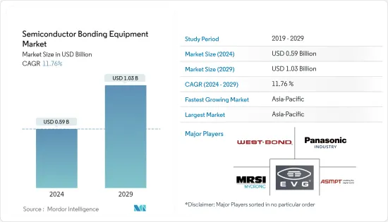
2024年半導體鍵合設備市場規模估計為5.9億美元,預計到2029年將達到10.3億美元,在預測期內(2024-2029年)CAGR為11.76%。
由於對具有更高效率、處理能力和更小占地面積的半導體晶片的需求不斷成長,半導體鍵合設備正在尋找應用,從而推動了預測期內的市場需求。
主要亮點
- 數位化對生活和商業的影響帶動了半導體市場的繁榮。這促使政府制定了支援 5G 部署的計劃。例如,歐盟委員會建立了公私合作夥伴關係來開發和研究 5G 技術。
- 隨著未來十年晶片需求的激增,預計到2030 年,全球半導體產業將成為兆美元的產業。這種成長很大程度上得益於在半導體製造、材料和研究方面大力投資的公司和國家,以確保穩定的發展。供應晶片和專業知識,以支持以數據為中心的行業的成長。
- 儘管全球疫情大流行並導致經濟低迷,但在各類晶片(尤其是成熟節點開發的晶片)需求激增的推動下,半導體產業仍保持韌性,2020年營收成長6.5%,達到4,400億美元大關。
- 半導體元件廣泛應用於大多數消費性電子產品。中國不僅是各種消費性電子產品的最大消費國和生產國之一,而且還透過出口多種主要用於生產製成品的投入品來滿足廣泛的國家需求。
- COVID-19引發的封鎖的開始產生了對工作和教育連續性的基本需求,促使對筆記型電腦和個人電腦等計算設備的需求增加,因此,半導體鍵合設備市場的需求激增。
- 當產品需要鍵合兩個晶片或晶圓時,可以使用多種方法,其中選擇的鍵合製程是鍵合擁有成本的主要促進因素。與某些黏合製程相關的高擁有成本可能會限制市場成長。
半導體鍵合設備市場趨勢
功率IC和功率分立應用領域佔據重要市場佔有率
- 對高能源和高能源效率設備的需求不斷成長,加上無線和攜帶式電子產品的日益普及,以及由於向電氣化的轉變而在汽車行業中使用這些設備的增加,是推動汽車行業成長的一些關鍵因素。該段。
- 電源 IC 和分立元件的一項重要趨勢是高效率電源管理。新的系統架構提高了交流-直流電源適配器的效率,同時減少了其尺寸和組件數量。新的乙太網路供電 (PoE) 標準允許更高的電力傳輸,從而支援新設備類別的開發,例如連網照明。
- 穿戴式裝置的幾個方面,從基礎實體到最終用戶體驗,在推動消費者採用和接受方面發揮著至關重要的作用。離散半導體公司預計在產品設計階段了解課題和市場趨勢,從而保持競爭力。
- 使用具有更大遷移率和更高臨界擊穿電場的半導體(例如SiC)來降低功率損耗正在獲得越來越多的關注,特別是在電晶體系列以及肖特基勢壘二極體(SBD)、結型場效電晶體等電力電子元件中(JFET)和 MOSFET 電晶體。
- 此外,智慧型手機的傳輸速度正在急劇提高,需要電池模組來支援處理。分離式半導體正在尋找進入電源轉接器的途徑,由於電池供電設備的銷售,預計需求將會增加。
- 物聯網(IoT)應用的成長預計將推動離散半導體的銷售。例如,根據愛立信的數據,2022 年全球蜂窩物聯網連接數為 19 億,預計到 2027 年將成長到 55 億,期間CAGR為 19%。此外,無線通訊產業預計將隨著 5G 網路的擴展而成長。消費者升級手機/設備以進一步推動全球離散採用的可能性也顯示了第五代網路的發展。
亞太地區預計將成為成長最快的市場
- 亞太地區是市場的重要參與者,得益於國內主要供應商的策略投資和成熟的半導體產業,預計在預測期內將出現可觀的成長。 SIA表示,隨著晶片消費持續成長,未來四年亞太半導體市場規模將是美洲市場的三倍以上。
- 這一成長預計將受到該地區一些最大的半導體公司的推動,以及支持中國、印度和越南等國家半導體產業基礎設施的投資不斷增加。此外,國內知名供應商和政府機構正在大力投資提供下一代半導體鍵合解決方案,例如混合鍵合,預計將增加市場需求。
- 例如,Xperi Holding Corporation 最近推出的智慧財產權 (IP) 授權業務品牌 Adeia 與 ROHM 集團子公司 LAPIS Technology 於 2022 年 5 月宣布達成協議,其中包括 Adeia 的 DBI Ultra 晶片的技術轉移- 晶圓混合鍵合技術支援該技術的開發和部署到LAPIS 的產品線。該協議還包括 Adeia 基礎混合鍵結專利組合的許可。
- 隨著國內晶片需求的不斷擴大,預計中國將取代美國成為全球半導體產業第一強國。根據半導體產業協會預測,到2030年,半導體市場規模將翻倍,達到1兆美元以上,其中中國貢獻了60%以上。這種指數級成長預計將增加對半導體鍵合設備的需求。
- 此外,2022年12月,中國宣布了一項價值超過1兆元人民幣(1,430億美元)的半導體產業支援計劃,顯著提高了晶片自給自足率,並對美國阻礙其技術發展的行為進行報復。大部分財政援助將用於資助中國企業購買本地半導體設備,預計將支持區域市場需求。
半導體鍵結設備產業概況
半導體鍵合設備市場高度分散,主要參與者包括 EV Group、ASMPT Semiconductor Solutions 和 MRSI Systems (Myronic AB),以及 WestBond Inc. 和 Panasonic Industry。這些市場參與者正在實施各種策略,例如合作夥伴關係、創新、投資和收購,以增強其產品供應並獲得永續的競爭優勢。
2022 年 11 月,SUSS MicroTec SE 為一種稱為脈衝電流鍵合的新型低溫場輔助鍵合技術鋪平了道路。這家瑞士大學的衍生公司基於一項重大科學發現開發了 Sy&Se 技術,並將適用於手動和自動晶圓鍵合機系統。電流脈衝鍵合結合了陽極鍵合的堅固性和其他更複雜的鍵結方法的材料多功能性。
2022 年 8 月,EV Group 擴大了與工業技術研究院(位於台灣新竹的重要應用技術研究機構)的合作,開發先進的異質整合製程。作為Hi-CHIP聯盟的成員,EVG集團提供了多種晶圓鍵合和光刻系統,包括GEMINI FB混合鍵合系統和EVG 850 DB自動解鍵系統。
額外的好處:
- Excel 格式的市場估算 (ME) 表
- 3 個月的分析師支持
目錄
第 1 章:簡介
- 研究假設和市場定義
- 研究範圍
第 2 章:研究方法
第 3 章:執行摘要
第 4 章:市場洞察
- 市場概況
- 市場吸引力 - 波特五力分析
- 供應商的議價能力
- 買家的議價能力
- 新進入者的威脅
- 替代品的威脅
- 競爭激烈程度
- 產業價值鏈分析
- COVID-19 對市場的影響
第 5 章:市場動態
- 市場驅動力
- 半導體製造商增加投資以擴大製造能力
- 各種應用對半導體晶片的需求不斷成長
- 市場限制
- 擁有成本高
- 電路小型化導致複雜度增加
第 6 章:市場區隔
- 依類型
- 永久黏合設備
- 臨時黏接設備
- 混合鍵合設備
- 依應用
- 先進封裝
- 電源IC和功率分立元件
- 光子裝置
- MEMS 感測器和執行器
- 工程基材
- CMOS 影像感測器 (CIS)
- 依地理
- 北美洲
- 亞太地區
- 歐洲
- 世界其他地區
第 7 章:競爭格局
- 公司簡介
- EV Group
- ASMPT Semiconductor Solutions
- MRSI Systems. (Myronic AB)
- WestBond Inc.
- Panasonic Industry Co. Ltd.
- Palomar Technologies
- Dr. Tresky AG
- BE Semiconductor Industries NV
- Fasford Technology Co.Ltd (Fuji Group)
- Kulicke and Soffa Industries Inc.
- DIAS Automation (HK) Ltd
- Shibaura Mechatronics Corporation
- SUSS MicroTec SE
- Tokyo Electron Limited
第 8 章:投資分析
第 9 章:市場的未來
The Semiconductor Bonding Equipment Market size is estimated at USD 0.59 billion in 2024, and is expected to reach USD 1.03 billion by 2029, growing at a CAGR of 11.76% during the forecast period (2024-2029).
Semiconductor bonding equipment is finding applications due to the rising demand for semiconductor chips with higher efficiency, processing power, and smaller footprints, driving the demand for the market during the forecast period.
Key Highlights
- The impact of digitalization on lives and businesses has led to a boom in the semiconductor markets. This has resulted in government programs supporting the deployment of 5G. For instance, the European Commission established a public-private partnership to develop and research 5G technology.
- With chip demand set to surge over the coming decade, the global semiconductor industry is expected to become a trillion-dollar industry by 2030. This growth is largely favored by companies and countries investing heavily in semiconductor manufacturing, materials, and research to guarantee a steady supply of chips and know-how to support growth across data-centric industries.
- Despite the global pandemic and resulting economic downturn, the semiconductor industry remained resilient, with revenue growth of 6.5% to reach the USD 440 billion mark in 2020, driven by a spike in demand for all types of chips, especially those developed at mature nodes.
- Semiconductor components are widely deployed in most consumer electronics products. China is not only one of the largest consumers and producers of various consumer electronics products but also caters to a broad range of countries by exporting several input supplies that are essentially used to produce finished goods.
- The onset of the COVID-19-induced lockdown created a basic need for continuity of work and education, resulting in an increase in demand for computing devices such as laptops and PCs, and consequently, the semiconductor bonding equipment market experienced a surge in demand.
- When a product requires the bonding of two dies or wafers, several methods might be used, with the bonding process selected being the primary driver for the cost of ownership of bonding. The high cost of ownership associated with some bonding processes might restrict market growth.
Semiconductor Bonding Equipment Market Trends
Power IC and Power Discrete Application Segment Holds Significant Market Share
- The rising demand for high-energy and power-efficient devices, coupled with the increasing prevalence of wireless and portable electronic products and the increased use of these devices in the automotive industry due to the shift towards electrification, are some key factors driving the growth of the segment.
- One significant trend in power IC and discrete is efficient power management. New system architectures improve the efficiency of AC-DC power adapters while reducing their size and component count. New Power-over-Ethernet (PoE) standards allow higher power transfer, enabling the development of new device classes, such as connected lighting.
- Several aspects of wearable devices, from the underlying physics to the end-user experience, play crucial roles in driving consumer adoption and acceptance. Discrete semiconductor companies poised to benefit from being aware of the challenges and market trends during the design phase of products to stay competitive.
- The use of semiconductors with larger mobility and higher critical breakdown fields, such as SiC, to reduce power losses is gaining traction, particularly among the transistor range, as well as power electronics devices like Schottky barrier diodes (SBDs), junction field-effect transistors (JFETs), and MOSFET transistors.
- Additionally, smartphone transmission speeds are dramatically increasing, requiring battery modules to support processing. Discrete semiconductors are finding their way into power adapters, with an expected increase in demand due to the sale of battery-powered devices.
- The growth of Internet of Things (IoT) applications is expected to boost the sales of discrete semiconductors. For instance, as per Ericsson, there were 1.9 billion cellular IoT connections worldwide in 2022, which is expected to grow to 5.5 billion in 2027, registering a CAGR of 19% over the period. Moreover, the wireless communications sector is expected to grow with the expansion of 5G networks. The likelihood of consumers upgrading their handsets/devices to drive discrete adoption further globally is also indicative of fifth-generation networks.
Asia Pacific is Expected to be the Fastest Growing Market
- The Asia Pacific region is a significant player in the market and is expected to experience considerable growth over the forecast period, thanks to strategic investments by key domestic suppliers and the well-established semiconductor sector. According to SIA, the Asia-Pacific semiconductor market is set to be more than three times the size of the Americas market over the next four years as chip consumption continues to rise.
- This growth is expected to be fueled by some of the largest semiconductor companies located in the region, as well as growing investments to support the semiconductor industry infrastructure across nations like China, India, and Vietnam. In addition, well-known domestic vendors and government agencies are making significant technological investments in offering next-generation semiconductor bonding solutions, such as hybrid bonding, which is expected to increase market demand.
- For example, Adeia, the recently launched brand for the intellectual property (IP) licensing business of Xperi Holding Corporation, and LAPIS Technology Co., Ltd., a subsidiary of the ROHM Group, announced an agreement in May 2022 that includes a technology transfer of Adeia's DBI Ultra die-to-wafer hybrid bonding know-how to support the development and deployment of the technology into LAPIS's product line. The agreement also includes a license to Adeia's underlying hybrid bonding patent portfolio.
- China is predicted to overtake the United States as the world's top powerhouse in the semiconductor industry based on its expanding domestic chip demand. According to the Semiconductor Industry Association, the semiconductor market will double in size to reach more than USD 1 trillion by 2030, with China contributing over 60% of that increase. This exponential growth is expected to increase demand for semiconductor bonding equipment.
- Furthermore, in December 2022, China announced a support program worth more than CNY 1 trillion (USD 143 billion) for its semiconductor industry, significantly advancing chip self-sufficiency and retaliating against American efforts to obstruct its technological development. Most of the financial assistance would be used to finance the purchases of local semiconductor equipment by Chinese enterprises, which is expected to support regional market demand.
Semiconductor Bonding Equipment Industry Overview
The Semiconductor Bonding Equipment Market is highly fragmented, with major players such as EV Group, ASMPT Semiconductor Solutions, and MRSI Systems (Myronic AB), as well as WestBond Inc. and Panasonic Industry Co. Ltd. These market players are implementing various strategies, such as partnerships, innovations, investments, and acquisitions, to enhance their product offerings and gain a sustainable competitive advantage.
In November 2022, SUSS MicroTec SE paved the way for a novel low-temperature field-assisted bonding technology called Impulse Current Bonding. The Swiss university spin-off has developed Sy&Se technology based on a significant scientific discovery and will be available on both manual and automatic wafer bonder systems. The current impulse bonding combines the robustness of anodic bonding with the material versatility of other, more complex bonding methods.
In August 2022, EV Group expanded its collaboration with the Industrial Technology Research Institute, a significant applied technology research institute based in Hsinchu, Taiwan, to develop advanced heterogeneous integration processes. As a member of the Hi-CHIP Alliance, EVG Group provided several wafer bonding and lithography systems, including the GEMINI FB hybrid bonding system and the EVG 850 DB automated debonding system.
Additional Benefits:
- The market estimate (ME) sheet in Excel format
- 3 months of analyst support
TABLE OF CONTENTS
1 INTRODUCTION
- 1.1 Study Assumptions and Market Definition
- 1.2 Scope of the Study
2 RESEARCH METHODOLOGY
3 EXECUTIVE SUMMARY
4 MARKET INSIGHTS
- 4.1 Market Overview
- 4.2 Market Attractiveness - Porter's Five Forces Analysis
- 4.2.1 Bargaining Power of Suppliers
- 4.2.2 Bargaining Power of Buyers
- 4.2.3 Threat of New Entrants
- 4.2.4 Threat of Substitutes
- 4.2.5 Intensity of Competitive Rivalry
- 4.3 Industry Value Chain Analysis
- 4.4 Impact of COVID-19 on the Market
5 Market Dynamics
- 5.1 Market Driver
- 5.1.1 Increasing Investment by Semiconductor Manufacturers to Expand their Manufacturing Capacity
- 5.1.2 Rising Demand for Semiconductor Chips across Various Application
- 5.2 Market Restraints
- 5.2.1 High Cost of Ownership
- 5.2.2 Increased Complexity Owing to Miniaturization of Circuits
6 MARKET SEGMENTATION
- 6.1 By Type
- 6.1.1 Permanent Bonding Equipment
- 6.1.2 Temporary Bonding Equipment
- 6.1.3 Hybrid Bonding Equipment
- 6.2 By Application
- 6.2.1 Advanced Packaging
- 6.2.2 Power IC and Power Discrete
- 6.2.3 Photonic Devices
- 6.2.4 MEMS Sensors and Actuators
- 6.2.5 Engineered Substrates
- 6.2.6 CMOS Image Sensors (CIS)
- 6.3 By Geography
- 6.3.1 North America
- 6.3.2 Asia Pacific
- 6.3.3 Europe
- 6.3.4 Rest of the World
7 COMPETITIVE LANDSCAPE
- 7.1 Company Profiles
- 7.1.1 EV Group
- 7.1.2 ASMPT Semiconductor Solutions
- 7.1.3 MRSI Systems. (Myronic AB)
- 7.1.4 WestBond Inc.
- 7.1.5 Panasonic Industry Co. Ltd.
- 7.1.6 Palomar Technologies
- 7.1.7 Dr. Tresky AG
- 7.1.8 BE Semiconductor Industries NV
- 7.1.9 Fasford Technology Co.Ltd (Fuji Group)
- 7.1.10 Kulicke and Soffa Industries Inc.
- 7.1.11 DIAS Automation (HK) Ltd
- 7.1.12 Shibaura Mechatronics Corporation
- 7.1.13 SUSS MicroTec SE
- 7.1.14 Tokyo Electron Limited
8 INVESTMENT ANALYSIS
9 FUTURE OF THE MARKET
 2023-2030 年全球半導體鍵結市場規模研究與預測(按類型、製程類型、鍵結技術、應用和區域分析)
 半導體鍵合設備市場報告:2030 年趨勢、預測與競爭分析
 晶片邦定機設備市場報告:2030 年趨勢、預測與競爭分析
 晶粒邦定機市場報告:2030 年趨勢、預測與競爭分析
 半導體鍵結市場:按類型、應用分類 - 2024-2030 年全球預測
 半導體鍵結市場 - 2018-2028 年全球產業規模、佔有率、趨勢、機會與預測,按類型、製程類型、鍵結技術、按應用、按競爭進行細分。
 2023-2030年全球半導體接合設備市場規模研究與預測,按類型、應用和區域分析
 半導體鍵結全球市場規模、佔有率、產業趨勢分析報告:用途、類型、鍵結技術、製程類型、區域展望與預測,2023-2030
 銲線機設備的全球市場
 貼片機設備的全球市場