

 |
市場調查報告書
商品編碼
1913281
穿透矽通孔(TSV)技術市場機會、成長促進因素、產業趨勢分析及預測(2026-2035)Through-Silicon Via (TSV) Technology Market Opportunity, Growth Drivers, Industry Trend Analysis, and Forecast 2026 - 2035 |
||||||
全球穿透矽通孔(TSV) 技術市場預計到 2025 年將達到 31 億美元,到 2035 年將達到 237 億美元,複合年成長率為 22.5%。
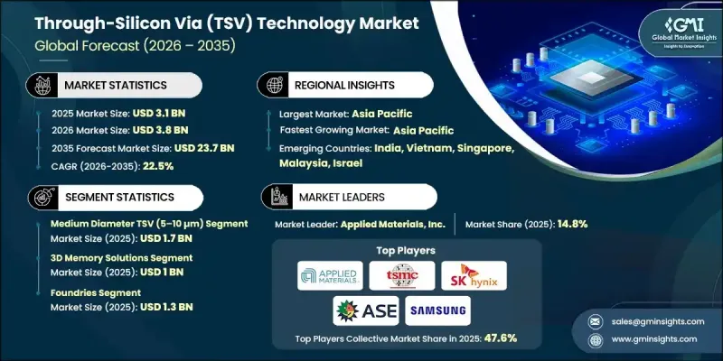
對緊湊、節能型半導體解決方案日益成長的需求正在重塑全球晶片設計策略。先進無線網路的廣泛應用推動了邊緣設備和行動平台性能要求的不斷提高,從而需要更小的尺寸和更高的頻寬效率。 TSV 技術實現了垂直整合,在外形規格尺寸的同時提升了電氣性能。隨著較小製程節點的經濟和技術限制日益凸顯,製造商正逐漸放棄傳統的平面縮放方式。3D架構和基於晶片組的設計正成為提升性能的永續途徑。自 1990 年代末期以來,堆疊式記憶體和感測器架構的採用一直在穩步加速。到 21 世紀 20 年代初,大多數整合設備製造商已將支援 TSV 的3D設計納入其長期性能規劃。展望未來十年,垂直堆疊將成為處理器和加速器發展的關鍵驅動力。同時,區域化的半導體生產和自動化主導的製造正在重塑 TSV 供應鏈。與銅填充、晶圓減薄和平面化差異相關的初始製程限制推動了整個製造流程的持續改進。
| 市場覆蓋範圍 | |
|---|---|
| 開始年份 | 2025 |
| 預測年份 | 2026-2035 |
| 起始值 | 31億美元 |
| 預測金額 | 237億美元 |
| 複合年成長率 | 22.5% |
中等直徑的矽通孔(TSV,5-10微米)佔據最大市場佔有率,預計2025年市場規模將達到17億美元。對小型化、熱效率和可靠供電的需求不斷成長,推動了先進3D封裝解決方案的普及。該領域的製造商正致力於提高製造精度、熱穩定性、能源效率和可擴展的成本結構,以支援半導體裝置密度的不斷提升。
預計到2025年,3D儲存解決方案市場規模將達10億美元。新一代高頻寬記憶體的商業化正在加速採用TSV技術的堆疊式儲存架構的普及。大規模運算環境的需求推動了對具有高速互連性能的垂直整合記憶體的需求,進一步凸顯了基於TSV的設計在低延遲資料處理方面的重要性。
美國穿透矽通孔(TSV)技術市場預計到2025年將達到5.12億美元,並在2026年至2035年間以22.3%的複合年成長率成長。聯邦政府投入527億美元支持國內製造業、外包半導體組裝測試以及先進封裝舉措。這項投資將促進TSV技術在記憶體、處理器和人工智慧加速器領域的應用,同時也有助於增強美國供應鏈的韌性。資料中心中晶片和高密度運算的日益普及進一步推動了市場需求,促使製造商將基礎設施投資與國內代工廠和雲端服務供應商對接。
目錄
第1章調查方法和範圍
第2章執行摘要
第3章業界考察
- 產業生態系分析
- 影響價值鏈的因素
- 利潤率分析
- 中斷
- 未來展望
- 製造商
- 經銷商
- 影響因素
- 成長促進因素
- 需要小型化的移動和 5G/Edge 設備
- 區域工廠和政府支持
- 人工智慧/高效能運算中的頻寬和密度需求
- 異質整合(晶片組、2.5D/3D積體電路)
- 製造業生態系的成熟度與資本投資
- 產業潛在風險與挑戰
- 製造成本、製程複雜性與產量比率損失
- 熱機械可靠性(熱膨脹係數 (CTE) 不匹配和應力)
- 機會
- 高效能運算 (HPC) 和人工智慧
- 3D堆疊式記憶體整合
- 成長促進因素
- 成長潛力分析
- 監管環境
- 北美洲
- 歐洲
- 亞太地區
- 拉丁美洲
- 中東和非洲
- 波特分析
- PESTEL 分析
- 科技與創新趨勢
- 當前技術趨勢
- 新興技術
- 新興經營模式
- 合規要求
- 永續性措施
- 消費者心理分析
- 專利和智慧財產權分析
- 地緣政治和貿易趨勢
第4章 競爭情勢
- 介紹
- 公司市佔率分析
- 按地區
- 北美洲
- 歐洲
- 亞太地區
- 拉丁美洲
- 中東和非洲
- 市場集中度分析
- 按地區
- 主要企業的競爭標竿分析
- 財務績效比較
- 收入
- 利潤率
- 研究與開發
- 產品系列比較
- 產品線豐富
- 科技
- 創新
- 按地區分類的企業發展比較
- 全球擴張分析
- 服務網路覆蓋範圍
- 按地區分類的市場滲透率
- 競爭定位矩陣
- 領導者
- 挑戰者
- 追蹤者
- 小眾玩家
- 戰略展望矩陣
- 財務績效比較
- 主要發展(2022-2025)
- 併購
- 夥伴關係與合作
- 技術進步
- 業務拓展與投資策略
- 永續發展計劃
- 數位轉型計劃
- 新興/Start-Ups競賽的趨勢
第5章 市場估算與預測:依TSV製程分類(2022-2035年)
- Via-first TSV
- VIA MiddleTSV
- 後導孔 TSV
第6章 市場估算與預測:依TSV直徑分類(2022-2035年)
- 大直徑TSV(超過10微米)
- 中等直徑的TSV(5-10微米)
- 小直徑TSV(小於5微米)
第7章 市場估計與預測:依應用領域分類(2022-2035 年)
- 3D 儲存解決方案
- 高頻寬體(HBM)
- 寬 I/O 內存
- 3D NAND快閃記憶體
- 處理器和計算設備
- CPU
- GPU
- 人工智慧加速器
- FPGA
- CMOS影像感測器
- MEMS元件
- 慣性感測器
- 壓力感測器
- 麥克風
- 其他
- 射頻(RF)和通訊設備
- 其他
第8章 依最終用途產業分類的市場估算與預測(2022-2035 年)
- 整合裝置製造商(IDM)
- 鑄造廠
- OSAT(半導體組裝測試服務)
- 無晶圓廠半導體公司
- 其他
第9章 各地區市場估算與預測(2022-2035 年)
- 北美洲
- 美國
- 加拿大
- 歐洲
- 英國
- 德國
- 法國
- 義大利
- 西班牙
- 俄羅斯
- 亞太地區
- 中國
- 印度
- 日本
- 韓國
- 澳洲
- 拉丁美洲
- 巴西
- 墨西哥
- 中東和非洲
- 南非
- 沙烏地阿拉伯
- 阿拉伯聯合大公國
第10章:公司簡介
- 主要企業
- Applied Materials, Inc.
- Samsung
- Taiwan Semiconductor Manufacturing Company Limited
- SK Hynix
- Intel Corporation
- Lam Research
- Toshiba Corporation
- ASE Group
- 按地區分類的主要企業
- 北美洲
- Amkor Technology
- Atomica Corp
- 歐洲
- Okmetic Oyj
- Imec
- 亞太地區
- Japan Semiconductor Corporation
- Powertech Technology
- 北美洲
- 小眾玩家/顛覆者
- Teledyne DALSA
- Nanosystems JP
The Global Through-Silicon Via (TSV) Technology Market was valued at USD 3.1 billion in 2025 and is estimated to grow at a CAGR of 22.5% to reach USD 23.7 billion by 2035.
Rising demand for compact, power-efficient semiconductor solutions continues to reshape chip design strategies worldwide. Increased deployment of advanced wireless networks places greater performance expectations on edge devices and mobile platforms, driving the need for smaller footprints and higher bandwidth efficiency. TSV technology enables vertical integration that reduces form factor size while improving electrical performance. Manufacturers increasingly shift away from conventional planar scaling as economic and technical limitations emerge at smaller nodes. Three-dimensional architectures and chiplet-based designs gain traction as viable pathways to sustain performance gains. Since the late 1990s, the adoption of stacked memory and sensor architectures steadily accelerated. By the early 2020s, most integrated device manufacturers incorporate TSV-enabled three-dimensional designs into long-term performance planning. Toward the next decade, vertical stacking becomes a primary driver of advancement for processors and accelerators. At the same time, regionalized semiconductor production and automation-driven manufacturing reshape TSV supply chains. Early process limitations related to copper filling, wafer thinning, and planarization variability drive continuous improvement efforts across fabrication workflows.
| Market Scope | |
|---|---|
| Start Year | 2025 |
| Forecast Year | 2026-2035 |
| Start Value | $3.1 Billion |
| Forecast Value | $23.7 Billion |
| CAGR | 22.5% |
The medium diameter TSVs, ranging from 5 to 10 micrometers, represent the largest segment and generated USD 1.7 billion in 2025. Growing requirements for miniaturization, thermal efficiency, and reliable power delivery encourage broader adoption of advanced three-dimensional packaging solutions. Manufacturers in this segment focus on achieving precision manufacturing, thermal stability, energy efficiency, and scalable cost structures to support rising volumes of high-density semiconductor devices.
The three-dimensional memory solutions segment generated USD 1 billion in 2025. Commercial availability of next-generation high-bandwidth memory accelerates the use of TSV-enabled stacked memory architectures. Demand from large-scale computing environments increases the need for vertically integrated memory with fast interconnect performance, reinforcing the importance of TSV-based designs for low-latency data processing.
U.S. Through-Silicon Via (TSV) Technology Market reached USD 512 million in 2025 and is projected to grow at a CAGR of 22.3% from 2026 to 2035. Federal funding of USD 52.7 billion supports domestic fabrication, outsourced semiconductor assembly and testing, and advanced packaging initiatives. This investment strengthens TSV adoption across memory, processors, and artificial intelligence accelerators while supporting national supply chain resilience. Expanding use of chiplets and high-density computing in data centers further drives demand, encouraging manufacturers to align infrastructure investments with domestic foundries and cloud service providers.
Key companies active in the Global Through-Silicon Via (TSV) Technology Market include Taiwan Semiconductor Manufacturing Company Limited, Intel Corporation, Applied Materials, Inc., Samsung, ASE Group, Lam Research, Amkor Technology, SK Hynix, Toshiba Corporation, Powertech Technology, Okmetic Oyj, Teledyne DALSA, Atomica Corp, Japan Semiconductor Corporation, Nanosystems JP, and imec. Companies operating in the Global Through-Silicon Via (TSV) Technology Market strengthen their competitive position through sustained investment in advanced packaging research, process automation, and yield optimization. Strategic collaboration across foundries, OSATs, and system designers supports faster adoption of three-dimensional integration. Many players focus on co-development frameworks to align TSV architectures with next-generation processors and memory platforms. Expanding localized manufacturing capacity improves supply chain security and reduces production risk. Firms also emphasize scalable process technologies that lower the cost per interconnect while improving reliability.
Table of Contents
Chapter 1 Methodology & Scope
- 1.1 Market scope and definition
- 1.2 Research design
- 1.2.1 Research approach
- 1.2.2 Data collection methods
- 1.3 Data mining sources
- 1.3.1 Global
- 1.3.2 Regional/Country
- 1.4 Base estimates and calculations
- 1.4.1 Base year calculation
- 1.4.2 Key trends for market estimation
- 1.5 Primary research and validation
- 1.5.1 Primary sources
- 1.6 Forecast model
- 1.7 Research assumptions and limitations
Chapter 2 Executive Summary
- 2.1 Industry 360° synopsis
- 2.2 Key market trends
- 2.2.1 TSV process trends
- 2.2.2 TSV diameter trends
- 2.2.3 Application trends
- 2.2.4 End-use industry trends
- 2.2.5 Regional trends
- 2.3 TAM Analysis, 2026-2035 (USD Billion)
- 2.4 CXO perspectives: Strategic imperatives
- 2.4.1 Executive decision points
- 2.4.2 Critical Success Factors
- 2.5 Future Outlook and Strategic Recommendations
Chapter 3 Industry Insights
- 3.1 Industry ecosystem analysis
- 3.1.1 Factor affecting the value chain
- 3.1.2 Profit margin analysis
- 3.1.3 Disruptions
- 3.1.4 Future outlook
- 3.1.5 Manufacturers
- 3.1.6 Distributors
- 3.2 Impact forces
- 3.2.1 Growth drivers
- 3.2.1.1 Mobile & 5G / edge devices needing miniaturization
- 3.2.1.2 Regional fabs and government support
- 3.2.1.3 AI / HPC demand for bandwidth & density
- 3.2.1.4 Heterogeneous integration (chiplets, 2.5D/3D ICs)
- 3.2.1.5 Manufacturing ecosystem maturation & equipment investment
- 3.2.2 Industry pitfalls & challenges
- 3.2.2.1 Manufacturing cost, process complexity & yield loss
- 3.2.2.2 Thermo-mechanical reliability (CTE mismatch & stress)
- 3.2.3 Opportunities
- 3.2.3.1 High-Performance Computing (HPC) & AI
- 3.2.3.2 3D Stacked Memory Integration
- 3.2.1 Growth drivers
- 3.3 Growth potential analysis
- 3.4 Regulatory landscape
- 3.4.1 North America
- 3.4.2 Europe
- 3.4.3 Asia Pacific
- 3.4.4 Latin America
- 3.4.5 Middle East & Africa
- 3.5 Porter's analysis
- 3.6 PESTEL analysis
- 3.7 Technology and Innovation landscape
- 3.7.1 Current technological trends
- 3.7.2 Emerging technologies
- 3.8 Emerging Business Models
- 3.9 Compliance Requirements
- 3.10 Sustainability Measures
- 3.11 Consumer Sentiment Analysis
- 3.12 Patent and IP analysis
- 3.13 Geopolitical and trade dynamics
Chapter 4 Competitive Landscape, 2025
- 4.1 Introduction
- 4.2 Company market share analysis
- 4.2.1 By region
- 4.2.1.1 North America
- 4.2.1.2 Europe
- 4.2.1.3 Asia Pacific
- 4.2.1.4 Latin America
- 4.2.1.5 Middle East & Africa
- 4.2.2 Market Concentration Analysis
- 4.2.1 By region
- 4.3 Competitive Benchmarking of key Players
- 4.3.1 Financial Performance Comparison
- 4.3.1.1 Revenue
- 4.3.1.2 Profit Margin
- 4.3.1.3 R&D
- 4.3.2 Product Portfolio Comparison
- 4.3.2.1 Product Range Breadth
- 4.3.2.2 Technology
- 4.3.2.3 Innovation
- 4.3.3 Geographic Presence Comparison
- 4.3.3.1 Global Footprint Analysis
- 4.3.3.2 Service Network Coverage
- 4.3.3.3 Market Penetration by Region
- 4.3.4 Competitive Positioning Matrix
- 4.3.4.1 Leaders
- 4.3.4.2 Challengers
- 4.3.4.3 Followers
- 4.3.4.4 Niche Players
- 4.3.5 Strategic outlook matrix
- 4.3.1 Financial Performance Comparison
- 4.4 Key developments, 2022-2025
- 4.4.1 Mergers and Acquisitions
- 4.4.2 Partnerships and Collaborations
- 4.4.3 Technological Advancements
- 4.4.4 Expansion and Investment Strategies
- 4.4.5 Sustainability Initiatives
- 4.4.6 Digital Transformation Initiatives
- 4.5 Emerging/ Startup Competitors Landscape
Chapter 5 Market Estimates & Forecast, By TSV Process Type, 2022-2035 (USD Billion)
- 5.1 Key trends
- 5.2 Via-First TSV
- 5.3 Via-Middle TSV
- 5.4 Via-Last TSV
Chapter 6 Market Estimates & Forecast, By TSV Diameter, 2022-2035 (USD Billion)
- 6.1 Key trends
- 6.2 Large diameter TSV (>10 µm)
- 6.3 Medium diameter TSV (5-10 µm)
- 6.4 Small diameter TSV (<5 µm)
Chapter 7 Market Estimates & Forecast, By Application, 2022-2035 (USD Billion)
- 7.1 Key trends
- 7.2 3D memory solutions
- 7.2.1 High bandwidth memory (HBM)
- 7.2.2 Wide I/O memory
- 7.2.3 3D NAND flash memory
- 7.3 Processors & compute devices
- 7.3.1 CPUs
- 7.3.2 GPUs
- 7.3.3 AI Accelerators
- 7.3.4 FPGAs
- 7.4 CMOS image sensors
- 7.5 MEMS devices
- 7.5.1 Inertial sensors
- 7.5.2 Pressure sensors
- 7.5.3 Microphones
- 7.5.4 Others
- 7.6 RF & communication devices
- 7.7 Others
Chapter 8 Market Estimates & Forecast, By End Use Industry, 2022-2035 (USD Billion)
- 8.1 Key trends
- 8.2 Integrated device manufacturers (IDMs)
- 8.3 Foundries
- 8.4 OSATs (Outsourced semiconductor assembly & test)
- 8.5 Fabless semiconductor companies
- 8.6 Others
Chapter 9 Market Estimates & Forecast, By Region, 2022-2035 (USD Billion)
- 9.1 Key trends
- 9.2 North America
- 9.2.1 U.S.
- 9.2.2 Canada
- 9.3 Europe
- 9.3.1 UK
- 9.3.2 Germany
- 9.3.3 France
- 9.3.4 Italy
- 9.3.5 Spain
- 9.3.6 Russia
- 9.4 Asia Pacific
- 9.4.1 China
- 9.4.2 India
- 9.4.3 Japan
- 9.4.4 South Korea
- 9.4.5 Australia
- 9.5 Latin America
- 9.5.1 Brazil
- 9.5.2 Mexico
- 9.6 MEA
- 9.6.1 South Africa
- 9.6.2 Saudi Arabia
- 9.6.3 UAE
Chapter 10 Company Profiles
- 10.1 Global Key Players
- 10.1.1 Applied Materials, Inc.
- 10.1.2 Samsung
- 10.1.3 Taiwan Semiconductor Manufacturing Company Limited
- 10.1.4 SK Hynix
- 10.1.5 Intel Corporation
- 10.1.6 Lam Research
- 10.1.7 Toshiba Corporation
- 10.1.8 ASE Group
- 10.2 Regional Key Players
- 10.2.1 North America
- 10.2.1.1 Amkor Technology
- 10.2.1.2 Atomica Corp
- 10.2.2 Europe
- 10.2.2.1 Okmetic Oyj
- 10.2.2.2 Imec
- 10.2.3 Asia Pacific
- 10.2.4 Japan Semiconductor Corporation
- 10.2.5 Powertech Technology
- 10.2.1 North America
- 10.3 Niche Players/Disruptors
- 10.3.1 Teledyne DALSA
- 10.3.2 Nanosystems JP
 2026年全球半導體封裝市場報告
 3-D TSV:關鍵問題洞察與市場分析
 半導體封裝市場規模、佔有率、趨勢和預測:按類型、封裝材料、技術、最終用戶和地區分類,2026-2034年
 高密度封裝(MCM、MCP、SIP、3D-TSV):市場分析與技術趨勢
 全球防靜電載帶捲市場(按載帶類型、材料、膠帶材料成分、膠帶層數和最終用途產業分類)預測(2026-2032年)導線架固定膠帶市場(按黏合劑類型、背襯材料、膠頻寬度、膠帶厚度、應用、最終用途行業和銷售管道),全球預測,2026-2032年
 MEMS封裝焊料市場規模、佔有率和成長分析:按焊料類型、產品形式、應用、封裝類型、最終用戶和地區分類 - 2026-2033年產業預測
 先進半導體封裝市場分析及預測(至2035年):依類型、產品類型、服務、技術、應用、材料類型、裝置、製程、最終用戶及功能分類半導體原型製作及封裝市場分析及預測(至2035年):依類型、產品類型、服務、技術、應用、材料類型、組件、製程、最終用戶、設備分類半導體封裝市場分析及預測(至2035年):依類型、產品類型、技術、應用、材料類型、裝置、製程、最終用戶、功能、設備分類